EP1172908A2 - Anordnung zur Leitungsverbindung - Google Patents
Anordnung zur Leitungsverbindung Download PDFInfo
- Publication number
- EP1172908A2 EP1172908A2 EP01117032A EP01117032A EP1172908A2 EP 1172908 A2 EP1172908 A2 EP 1172908A2 EP 01117032 A EP01117032 A EP 01117032A EP 01117032 A EP01117032 A EP 01117032A EP 1172908 A2 EP1172908 A2 EP 1172908A2
- Authority
- EP
- European Patent Office
- Prior art keywords
- wiring
- connecting portion
- main
- elbow
- bus bar
- Prior art date
- Legal status (The legal status is an assumption and is not a legal conclusion. Google has not performed a legal analysis and makes no representation as to the accuracy of the status listed.)
- Granted
Links
Images











Classifications
-
- H—ELECTRICITY
- H02—GENERATION; CONVERSION OR DISTRIBUTION OF ELECTRIC POWER
- H02B—BOARDS, SUBSTATIONS OR SWITCHING ARRANGEMENTS FOR THE SUPPLY OR DISTRIBUTION OF ELECTRIC POWER
- H02B1/00—Frameworks, boards, panels, desks, casings; Details of substations or switching arrangements
- H02B1/20—Bus-bar or other wiring layouts, e.g. in cubicles, in switchyards
-
- H—ELECTRICITY
- H10—SEMICONDUCTOR DEVICES; ELECTRIC SOLID-STATE DEVICES NOT OTHERWISE PROVIDED FOR
- H10W—GENERIC PACKAGES, INTERCONNECTIONS, CONNECTORS OR OTHER CONSTRUCTIONAL DETAILS OF DEVICES COVERED BY CLASS H10
- H10W44/00—Electrical arrangements for controlling or matching impedance
- H10W44/501—Inductive arrangements
-
- H—ELECTRICITY
- H10—SEMICONDUCTOR DEVICES; ELECTRIC SOLID-STATE DEVICES NOT OTHERWISE PROVIDED FOR
- H10W—GENERIC PACKAGES, INTERCONNECTIONS, CONNECTORS OR OTHER CONSTRUCTIONAL DETAILS OF DEVICES COVERED BY CLASS H10
- H10W70/00—Package substrates; Interposers; Redistribution layers [RDL]
- H10W70/60—Insulating or insulated package substrates; Interposers; Redistribution layers
- H10W70/62—Insulating or insulated package substrates; Interposers; Redistribution layers characterised by their interconnections
- H10W70/65—Shapes or dispositions of interconnections
- H10W70/658—Shapes or dispositions of interconnections for devices provided for in groups H10D8/00 - H10D48/00
Definitions
- the present invention relates to a structure of wiring connection, and more particularly to a structure of wiring connection applied to plate-like electric wirings called as bus bars.
- the two bus bars that flow currents of equal magnitude and of opposite directions to each other are structured in layers and in parallel to be closer as possible, like a bus bar 101 and a bus bar 102 in Fig.42, which is one of ordinary-seen example of such bus bar formations.
- a bus bar 101 and a bus bar 102 in Fig.42 which is one of ordinary-seen example of such bus bar formations.
- each bus bar has to have a "connecting portion" for it.
- the bus bar 101 and the bus bar 102 in Fig. 42 were internal wirings, a bus bar 111 and a bus bar 112 are to be the external ones.
- the bus bar 101 is to connect with the bus bar 111, and the bus bar 102 is to connect with the bus bar 112.
- the external wirings should have the same or similar structures and formation as those of the internal wirings, if reduction of inductance in an entire electric circuit is intended. And connection of these bus bars should be carried out by, for instance, fastening with bolts and nuts considering ease of assembly and maintenance.
- the present invention has been achieved through such consideration and an object of the invention is to provide a structure of wiring connection capable of suppressing an increase of inductance effectively.
- a structure of wiring connection has: a first wiring that extends as a narrow plate having two main faces and having a predetermined plate width, and provided with a main portion, at least one connecting portion and an elbow portion defined as a portion between the main portion and the connecting portion thereof; a second wiring that extends as a narrow plate having two main faces and having a predetermined plate width, and provided with a main portion, at least one connecting portion and an elbow portion defined as a portion between the main portion and the connecting portion thereof; a third wiring that extends as a narrow plate having two main faces and having a predetermined plate width, and provided with a main portion, at least one connecting portion and an elbow portion defined as a portion between the main portion and the connecting portion thereof, the connecting portion of the first wiring and the connecting portion of the third wiring being in contact with each other through a predetermined area; and a fourth wiring that extends as a narrow plate having two main faces and having a predetermined width, and provided with a main portion,
- a specific distance defined as a distance between gravity centers in sections of two corresponding wirings of the first wiring to the fourth wiring cut along a plane vertical to each main face of the two corresponding wirings is less than the predetermined plate width of each of the two corresponding wirings.
- each predetermined plate width of the first wiring to the fourth wiring is the same width.
- the elbow portion of the first wiring and that of the third wiring are in contact with each other, and the elbow portion of the second wiring and that of the fourth wiring are in contact with each other.
- the elbow portion of the first wiring and that of the third wiring are in contact with each other to be sandwiched between the elbow portion of the second wiring and that of the fourth wiring.
- each connecting portion of the first wiring to the fourth wiring is detachable from a corresponding connecting portion thereof.
- a structure of wiring connection has: a first wiring that extends as a narrow plate having two main faces and having a predetermined plate width, and provided with a main portion, at least one connecting portion and an elbow portion defined as a portion between the main portion and the connecting portion thereof; a second wiring that extends as a narrow plate having two main faces and having a predetermined plate width, and provided with a main portion, at least one connecting portion and an elbow portion defined as a portion between the main portion and the connecting portion thereof; a third wiring that extends as a narrow plate having two main faces and having a predetermined plate width, and provided with a main portion, at least one connecting portion and an elbow portion defined as a portion between the main portion and the connecting portion thereof; a fourth wiring that extends as a narrow plate having two main faces and having a predetermined plate width, and provided with a main portion, at least one connecting portion and an elbow portion defined as a portion between the main portion and the connecting portion thereof, the connecting portion of the first wiring and the connecting
- a specific distance defined as a distance between gravity centers in sections of two corresponding wirings of the first wiring to the sixth wiring cut along a plane vertical to each main face of the two corresponding wirings is less than the predetermined plate width of each of the two corresponding wirings.
- the main portion of the first wiring, the main portion of the second wiring and the main portion of the third wiring run together in parallel facing each one of main faces thereof, and the main portion of the fourth wiring, the main portion of the fifth wring and the main portion of the sixth wiring run together in parallel facing each one of main faces thereof.
- each predetermined plate width of the first wiring to the sixth wiring is the same width.
- the first wiring is provided with a region where part thereof is curved such that when the first wiring to the sixth wiring are in a circuit system, and the fourth wiring and the fifth wiring are connected with each other at somewhere therein, inductance for a current through the first wiring, the fourth wiring, the fifth wiring and to the second wiring is equal to inductance for a current through the third wiring, the sixth wiring, the fifth wiring and to the second wiring.
- part of the first wiring is provided with a region where the plate width thereof is changed such that when the first wiring to the sixth wiring are in a circuit system, and the fourth wiring and the fifth wiring are connected with each other at somewhere therein, inductance for a current through the first wiring, the fourth wiring, the fifth wiring and to the second wiring is equal to inductance for a current through the third wiring, the sixth wiring, the fifth wiring and to the second wiring.
- part of the first wiring is provided with a region where plate thickness thereof is increased such that when the first wiring to the sixth wiring are in a circuit system, and the fourth wiring and the fifth wiring are connected with each other at somewhere therein, inductance for a current through the first wiring, the fourth wiring, the fifth wiring and to the second wiring is equal to inductance for a current through the third wiring, the sixth wiring, the fifth wiring and to the second wiring.
- each connecting portion of the first wiring to the sixth wiring is detachable from a corresponding connecting portion thereof.
- the first wiring and the second wiring are used as internal wirings in an electric device module, and the connecting portion and the elbow portion of the first wiring and those of the second wiring are exposed on a surface of the electric device module.
- the connecting portion of the first wiring and that of the second wiring are provided on a surface of a box-like shell of the electric device module, while the electric device module is a power transistor module, a power diode module or an intelligent power module.
- elbow portions continuing each connecting portion of the first wiring and that of the second wiring are provided on the same surface of the box-like shell of the electric device module as that the connecting portions are provided.
- elbow portions continuing each connecting portion of the first wiring and that of the second wiring are provided on the adjoining surface of the box-like shell of the electric device module to that the connecting portions are provided.
- the first wiring to the third wiring are used as internal wirings of the electric device module, and the connecting portion and the elbow portion of the first wiring, those of the second wiring and those of the third wiring are respectively exposed on a surface of the electric device module.
- each connecting portion of the first wiring to the third wiring is provided on a surface of the box-like shell of the electric device module, while the electric device module is a power transistor module, a power diode module or an intelligent power module.
- a wiring connection method prepares first to fourth wirings that respectively extends as narrow plates each having two main faces and having a predetermined plate width, and provided with a main portion, at least one connecting portion and an elbow portion defined as a portion between the main portion and the connecting portion thereof; connects the connecting portion of the first wiring and the connecting portion of the third wiring so as to be in contact with each other through a predetermined area; and connects the connecting portion of the second wiring and the connecting portion of the fourth wiring so as to be in contact with each other through a predetermined area.
- a specific distance defined as a distance between gravity centers in sections of two corresponding wirings of the first wiring to the fourth wiring cut along a plane vertical to each main face of the two corresponding wirings is less than the predetermined plate width of each of the two corresponding wirings.
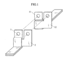
- Fig. 1 shows the structure of wiring connection of the first embodiment of the present invention.
- bus bars 1, 2, 11 and 12 each of which is a narrow metal plate having two main faces, and having a predetermined plate width.
- the bus bar 1 and bus bar 2 (corresponding to first and second wirings in the undermentioned claims) are running in parallel, and in layers and set close as possible but not contact with each other (such a formation is obtained, for instance, by using a thin insulating film, which is not shown in the figure).
- the bus bar 11 and the bus bar 12 (corresponding to third and fourth wirings in the undermentioned claims) are also provided in the same manner.
- the portion of a bus bar where the current of opposite direction to that flowing in the nearest portion of the partner bus bar can flow is defined as the main portion.
- each of the bus bar has the connecting portion that has at least one hole for fastening to others by a bolt and nut (not shown in Fig. 1), and has a predetermined electrically contacting area around the hole.
- the dashed lines in Fig. 1 predict these relationships, so that the bus bar 1 is to be fastened to and connected with the bus bar 11, and the bus bar 2 is to be fastened to and connected with the bus bar 12.
- the portion between the main portion and the connecting portion of a bus bar, which cannot be included by either definition, is called here the elbow portion.
- each bus bar is bent with a right angle at the end of each main portion or at the beginning of the elbow portion.
- the elbow portion of the bus bar 2 and that of the bus bar 12 are electrically contacted each other in this case, when they are fastened up.
- the current direction of the nearest portion of the bus bar 2 cannot obviously defined, and the same condition in the elbow portion of the bus bar 11 is encountered.
- the bus bar 1 and the bus bar 11 are fastened with riding over the elbow portion of the bus bar 2 and that of the bus bar 12 as shown in Fig. 1.
- the regular cross section of a narrow plate or a bus bar cut with a flat plane vertical to the direction that the narrow plate extends is called here the regular cross section.
- the shape of the regular cross section of the plate is a rectangle or the shape that can be regarded as almost a rectangle.
- the plate width can be defined as the length of the long side of the rectangle.
- the plate thickness can be defined as the length of the short side of the rectangle.
- the regular cross section of a plate is an ellipse or the shape that can be regarded as substantially an ellipse
- the plate width can be defined as the major axis of the ellipse
- the plate thickness can be defined as the minor axis of the ellipse.
- the specific distance between bus bars at the main portions is generally defined as the distance between the gravity centers of corresponding bus bar's cross sections cut along the flat plane vertical to the direction that the bus bars extends, and includes a point of either bus bar. If the bus bar has a corner like the bus bar 2 in Fig. 1, the locus of the gravity center can be defined along the line where the bus bar 2 extends.
- the specific distance is generally defined only between currents flowing along the direction where each bus bar extends. If current flows along the direction of the plate thickness like between the elbow portions of the bus bar 2 and the bus bar 12 in Fig. 1, the geometrically defined specific distance dose not generally have meaning, because it is generally for calculating the partial inductance between corresponding bus bars.
- the specific distance is especially defined as a distance between the gravity centers in the cross sections of two corresponding bas burs cut along a flat plane vertical to each main face of the two corresponding bus bars, and more especially such a specific distance is set to be less than the predetermined plate width of each of the two corresponding wirings.
- Such a novelly introduced specific distance is employed throughout the whole embodiments of the present invention.
- the bus bar 102 and the bus bar 112 are so constructed as to emerge laterally from a line, on which the bus bar 101 and the bus bar 111 extend, in such a manner that they have portions not contacting each other.
- each bus bar is 20 mm
- the thickness thereof is 2 mm
- the thickness of an insulating material sandwiched between the bus bar 101 and the bus bar 102 and between the bus bar 111 and the bus bar 112 is 1 mm
- the specific of a pair of the bus bars is 3 mm.
- the specific distance is at least 20 mm or more which is the width of each bus bar and the length of such a region is considered to be about three times the width of the bus bar.
- the bus bar 2 and the bus bar 12 overlap each other at each connecting portion having a flat portion in the surrounding of the fastening portion and also the elbow portion having a flat portion continuously therefrom, such that they are entirely in contact so as to ensure sufficient conductivity. Therefore, it has substantially the same structure as a state without any general connecting portion in which an emerging portion not overlapping the other bus bar is provided as seen in the structure of Fig. 42.
- the bus bar 1 and the bus bar 11 have the elbow portions riding over the elbow portions of the bus bar 2 and the bus bar 12, a sufficient conductivity is ensured through the flat portions in the surrounding of the fastening portions of the connecting portions thereof.
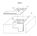
- FIG. 2 Such a concrete application example of this embodiment is shown in Fig. 2, and a comparative application example employing the structure shown in Fig. 42 is shown in Fig. 3.
- Fig. 3 will be referred to prior to Fig. 2 as a matter of convenience.
- Fig. 3 indicates the example of applying the structure shown in Fig. 42 to the bus bar of internal wire in the power transistor module.
- a difference between the structure shown in Fig. 2 and the structure shown in Fig. 3 is that a portion continuous from the fastening portion of each bus bar is also in the vicinity of its corresponding bus bar.
- each elbow portion is preferably provided, and any position to be included in the main portion, the connecting portion, and the elbow portion of any one of the bus bars 1, 2, 11 and 12 faces to at least one of the other bus bars such that the specific distance thereof is less than the width of each of the bus bars 1, 2, 11 and 12.
- the main portion of the bus bar 1 and the main portion of the bus bar 2 run together in parallel such that the main faces thereof face to each other in a condition that the specific distance thereof is less than the width of each of the bus bar 1 and the bus bar 2.
- the main portion of the bus bar 11 and the main portion of the bus bar 12 run together in parallel such that the main faces thereof face to each other in a condition that the specific distance thereof is less than the width of each of the bus bar 11 and the bus bar 12.
- inductance can be largely suppressed entirely as a structure of wire connection including respective bus bars.
- the connecting structure of this embodiment and also that of a second embodiment can be applied to not only the power transistor module but also the structure of the bus bar of internal wiring in the diode module for electric power (power diode module) or an intelligent power module (IPM), together with the structure of the bus bar of external wiring connected thereto.
- IPM intelligent power module
- each connecting occupies a relatively large area of the surface of the power transistor module.
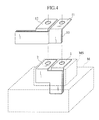
- the structure of a connecting portion shown in Fig. 4 may be employed.
- a portion MS for accommodating a nut corresponding to a bolt to be mounted from above in Fig. 4 is protruded from the surface of the power transistor module M.
- the connecting portions of the bus bar 1 and the bus bar 2 of internal wires are disposed on top of the nut accommodating portion MS.
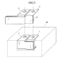
- the bus bar 1 and the bus bar 2 of the internal wirings are disposed on side faces of the nut accommodating portion MS, such that the L-letter shaped terminals are exposed.
- the bus bar 11 and the bus bar 12 of the external wirings formed in the L shape are mounted.
- reference numeral 10 in Fig. 4 denotes an insulating plate provided so as to block the bus bar 11 and the bus bar 2 from making contact with each other.
- inductance can be largely suppressed while restricting a connecting portion occupying area as an exclusively occupying area, effectively.
- the bus bar 1 and the bus bar 2 of the internal wirings are disposed on the side wall of the intelligent power module M such that they are exposed and combined with corresponding bus bar 11 and the bus bar 12, thereby making it possible to obtain a structure of the connecting portion having a low inductance.
- main portions of corresponding bus bar pairs may be extended in any directions from the overlapped elbow portions, and the above-mentioned structure as shown Fig. 1 is one example.
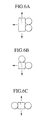
- Fig. 6A to Fig.6C are schematic diagrams explaining the variation of the relationship among connecting portions, elbow portions and main portions.
- each circle indicates each connecting portion fastened with each other.
- Each rectangle or square indicates the overlapped elbow portions.
- each arrow indicates the direction allowing each pair of the bus bars to extend their main portions.
- the two pairs of main portions can be extended along the same direction in these diagrams.
- each of them may be extended to any direction apart from the paper plane. Or it may be extended to the vertical direction to the paper plane.
- the structures shown in Fig. 1 and Fig. 2 correspond to the category of Fig. 6A.
- upper-side plate for instance, of a bus bar pair connects with the same-side plate of the other pair as shown in Fig. 1.
- upper-side plate of a bus bar pair connects with the bottom-side plate of the other pair, for instance, as shown in undermentioned Fig. 9.
- Fig. 7 shows the structure in which the bus bar corresponding to Fig. 6B is extended and Fig. 8 to Fig. 10 shows the structure in which the bus bar corresponding to Fig. 6C is extended.
- an increase of inductance becomes 2.45 nH if calculating with the specification described above as compared to a case where there is no connecting portion and elbow portion, so that it can be kept to about 1/10 the structure in Fig. 42.
- the up/down relation of the wiring is inverted by connection. If the structure shown in Fig. 10 is employed, this can be prevented.
- the increase of inductance is 5.06 nH, which is a little larger than the above case.
- Fig. 11 and Fig. 12 have almost the same effect as the structures described above. These do not have any elbow portion which rides over other bus bar, so that a flat configuration is used.
- the bus bar continuous to the connecting portion may be extended in any direction.
- two fastening portions are provided in each connecting portion thereby making more secure contact between the bus bars.
- the connecting portions of corresponding bus bars are in contact with each other so as to ensure a sufficient conductivity, and the connecting portions of the corresponding bus bars are continuous quickly to the main portions such that the main portions extend to face to each other.
- the elbow portions of the bus bars 1, 2, 11 and 12 are respectively minimized.
- the connecting portions of the bus bars 1, 2, 11 and 12 secure a sufficient conductivity and at any position of their main portions, the main face of the bus bar faces that of the other bus bar such that the specific distance is less than the width of each of the bus bars 1, 2, 11 and 12 and therefore, the increase of inductance in the connecting portion is substantially negligible. It can be estimated that this structure is an optimum structure for the power transistor module having the bus bars with the structure shown in Fig. 14.
- the connecting portion may use screw fastening or riveting and other press-fit system may be used depending on the necessity.
- Fig. 15 shows a bridge circuit which sends rectangular wave to a load L (for example, motor) to drive it, which is drawn here about only portions necessary for explanation.
- L for example, motor
- B indicates a battery
- P indicates positive potential wiring
- N indicates a ground wire corresponding thereto.
- the dashed line indicates a power transistor module, which is a set for achieving an actual circuit.
- two transistors T1 and T2 are synchronously turned ON/OFF. For example, at an instance when the transistor T1 gets conductive with the transistor T2, in the power transistor module in U phase, current flows from U to N. Then, if both the two transistors T1 and T2 are turned off, the current flows from U to P due to induced electromotive force in the load L in the power transistor module in U phase while no current flows to the ground line N.
- Fig. 15 functions as a chopper circuit for if the load L is a motor, making it produce a desired output.
- the structure of Fig. 15 functions as a chopper circuit for if the load L is a motor, making it produce a desired output.
- its transistor and wiring allocation relations are substantially the same.
- a portion of wiring indicated with a circle in Fig. 16 is a structure having the adjacent facing wirings but actually not a structure in which the opposing currents flow in the facing wirings.
- an effect of reducing inductance cannot be expected sufficiently.
- inductance of an output line of the power transistor module is in series with inductance of the load L connected forward and relatively small, it has been generally considered as negligible one.
- the inductance at such a portion has to be precisely considered.
- an arrow in Fig. 16 indicates a current path.
- FIG. 17 A structure achieved through the above described consideration to reduce inductance of the entire circuit is shown in Fig. 17. Incidentally, an arrow in Fig. 17 indicates a current path.
- the output line of the power transistor module in U phase and the output line of the power transistor module in V phase are disposed adjacent each other and then, the positive potential wire P and the ground wire N are made to run together up to a position where the output wire of the power transistor module in U phase is located adjacent the output wire of the power transistor module in V phase.
- these three wires are structured in three layers (three stage layered structure or three piece layered structure) in the order of P, U and N, a compact structure is provided and inductance of. the wire is reduced, which is preferable.
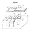
- Fig. 18 is a diagram in which a power transistor module in U phase and an external wiring connected thereto in Fig. 17 are drawn.
- the respective wires are layered in the order of P, U, and N outside the power transistor module M so that magnetic fields generated by respective wires are cancelled by the other thereby reducing wiring inductance.
- the connecting portion of the bus bar of an internal wiring is exposed on the surface of the power transistor module M.
- the arrangement in the connecting portion is in the order of P, N and U like a general power transistor module, of course, the order of P, U and N is permissible.
- reference numerals 1, 2, 3 in Fig. 18 denote bus bars of internal wirings corresponding successively to the wires P, U, N and the bus bars 1, 2 and 3 correspond to the first, second and third wires.
- the bus bars 11, 12 and 13 are bus bars of external wires corresponding thereto and correspond to fourth, fifth and sixth wires.
- the connecting portion of each bus bar has a fastening hole.
- the dashed line connecting the holes in the same figure indicates a correspondence relation.
- an insulating plate is sandwiched between the bus bars 1, 2, 3 and 13 at a portion except the fastening portion so as to ensure insulation upon connection. That is, the connecting portion of the bus bar 1 is connected to the connecting portion of the bus bar 12 such that they are in contact with each other through a predetermined area.
- the connecting portion of the bus bar 2 is connected to the connecting portion of the bus bar 12 such that they are in contact with each other through a predetermined area.
- the connection portion of the bus bar 3 is connected to the connecting portion of the bus bar 13 such that they are in contact with each other through a predetermined area. Because these connecting portions are to be connected with bolts and nuts, they can be detached.
- each of the bus bars 1, 2 and 3 is correspondingly shown in each of Fig. 19 to Fig. 21 so as to explain the wiring structure further in detail.
- Fig. 22 shows a view taken from the opposite side about the bus bars 11, 12 and 13 of the external wires.
- Fig. 23 shows a sectional view cut along a plane vertical to the surface of the power transistor module through the lines A-A as viewed in the direction of an arrow.
- Fig. 24 shows a sectional view cut along a plane vertical to the surface of the power transistor module through the lines B-B in Fig. 18.
- the bus bars are drawn in a condition that they are in contact with each other for convenience for explanation.
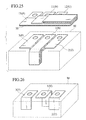
- bus bar of the internal wiring in the power transistor module as shown in Fig. 26, only the fastening portions of the bus bars 1, 2 and 3 are exposed on the surface of the power transistor module and following portions do not overlap, such that they are disposed separately. Under such a structure, however the bus bars of the external wirings are constructed, there is a limit for reduction of inductance in the connecting portion.
- each elbow portion is preferably provided, and any position to be included in the main portion, the connecting portion, and the elbow portion of any one of the bus bars 1, 2, 3, 11, 12 and 13 faces to at least one of the other bus bars such that the specific distance thereof is less than the width of each of the bus bars 1, 2, 3, 11, 12 and 13.
- the main portions of the bus bars 1, 2 and 3 run together in parallel with three layer structure, such that the main faces thereof face to each other and the specific distance thereof is less than the width of each of the bus bars 1, 2 and 3.
- the main portions of the bus bars 11, 12 and 13 run together in parallel with three layer structure, such that the main faces thereof face to each other and the specific distance thereof is less than the width of each of the bus bars 11, 12 and 13.
- Fig. 27 and Fig. 28 are perspective views for explaining flows of currents between P and U and between U and N in Fig. 18.
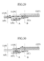
- Fig. 29 and Fig. 30 are the same sectional views as Fig. 23 and arrows in Fig. 29 and Fig. 30 indicate current flow, more specifically current flows between P and U, and between U and N.
- the length of each arrow indicates the magnitude corresponding to half the width of a corresponding bus bar. Because small currents which may be generated are negligible, a representation thereof is omitted.
- a "symbol of a circle containing a dot therein” and a “symbol containing a cross therein” are the same as vector notation, which mean a "direction coming to this way” and a “direction going to that way", both directions being at right angle to the paper.
- the point A indicates schematically a point where the wires running together in parallel (or currents flowing therein) in the "main portions" of the bus bars 1, 2 and 3 of internal wirings become unparalleled toward the "connecting portions" or a branch position.
- the point B corresponds to a position containing the same meaning as the point A in the bus bars 11, 12 and 13 of the external wirings.
- Fig. 18 shows an embodiment of a pattern in which the bus bar in Fig. 31A is extended.
- Fig. 32 shows an embodiment of a pattern in which the bus bar in Fig. 31D is extended. Patterns shown in Fig. 31B and Fig. 31C can be appropriately considered. Further, by considering whether or not arrangement of the bus bars is inverted by connection and whether the arrangement of the connecting terminals is P-N-U or P-U-N, a variety of patterns can be obtained.
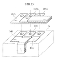
- the layer arrangement of the bus bars inside the power transistor module is inverse in a vertical direction to the structure of Fig. 18 and therefore, branching ways of the three bus bars are different.
- the same sectional views as Fig. 29 and Fig. 30 are expressed as shown in Fig. 34 and Fig. 35.
- unit of 8 is provided between P and U and unit of 12 is provided between U and N.
- a gap between the bus bar 3 and the bus bar 13 is adjusted appropriately so as to carry out fine adjustment of inductance.
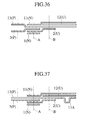
- the bus bar of side P is provided with a curved portion 13A which is curved in a direction vertical to the main face of the bus bar as shown in Fig. 37 or a curved region 13D which is curved in a direction parallel to the main face of the bus bar as shown in Fig. 38, thereby providing with a portion for locally increasing the specific distance. That is, under these structures, part of the bus bar 11 and the bus bar 13 is provided with a curved portion or a curved region so that inductance between wires when opposing current flow through the bus bar 1 and the bus bar 2 is substantially equal to inductance between wires when opposing currents flow through the bus bar 2 and the bus bar 3.
- a position where the curved portion 13A or the curved region 13D is provided is not restricted to a position shown in the same figure, but they may be provided in the vicinity of each fastening portion.
- the structure in which the bus bars are kept separate to each other according to the first adjustment method and the structure in which the curved portion 13A is provided according to the second adjustment method have the same meaning as employing a structure for adjusting the thickness of an insulating layer between the bus bars such that it is locally thick.
- a wide region 11 11C is provided in the bus bar 11 on the side of N as shown in Fig. 39 or a narrow region 13C is provided in the bus bar 13 on the side of P as shown in Fig. 40.
- a region in which the width of the bus bar is changed is provided on a side of the bus bar, of course, it is permissible to provide it on an opposite side or on both sides. That is, part of each of the bus bar 11 and the bus bar 13 is provided with a region in which the width of the plate is changed so that inductance between wires when opposing currents flow through the bus bar 1 and the bus bar 2 is substantially equal to inductance between wires when opposing currents flow through the bus bar 2 and the bus bar 3.
- a conductive plate 13B is attached to part of the bus bar 13 as shown in Fig. 41 so as to increase the plate width locally.
- Part of the bus bar 13 is provided with a plate thickness changing region in which the plate thickness is increased so that inductance between wires when opposing currents flow through the bus bar 1 and the bus bar 2 is equal to inductance between wires when opposing currents flow through the bus bar 2 and the bus bar 3.
- the region in which the plate thickness is increased may be integrated with the bus bar or so constructed that a detachable conductor is mounted thereon with bolts and nuts. If the detachable structure is employed, adjustment of inductance is enabled even after the bus bar is installed on a device.
- bus bar 1 and the bus bar 2 correspond to the first, second wires for convenience for description, of course, it is possible to interpret that the bus bar 1 and the bus bar 2 correspond to third, fourth wires while the bus bar 11 and the bus bar 12 correspond to the first, second wires.
- bus bars 1, 2 and 3 correspond to the first, second, third wires while the bus bars 11, 12 and 13 correspond to fourth, fifth, sixth wires for convenience for the description, of course, it is possible to interpret that the bus bars 1, 2 and 3 correspond to the fourth, fifth, sixth wires while the bus bars 11, 12 and 13 correspond to the first, second, third wires.
Landscapes
- Engineering & Computer Science (AREA)
- Power Engineering (AREA)
- Inverter Devices (AREA)
- Installation Of Bus-Bars (AREA)
- Structure Of Printed Boards (AREA)
- Connection Or Junction Boxes (AREA)
Applications Claiming Priority (2)
| Application Number | Priority Date | Filing Date | Title |
|---|---|---|---|
| JP2000212467 | 2000-07-13 | ||
| JP2000212467A JP3724345B2 (ja) | 2000-07-13 | 2000-07-13 | 配線の接続部構造 |
Publications (3)
| Publication Number | Publication Date |
|---|---|
| EP1172908A2 true EP1172908A2 (de) | 2002-01-16 |
| EP1172908A3 EP1172908A3 (de) | 2003-01-02 |
| EP1172908B1 EP1172908B1 (de) | 2014-11-12 |
Family
ID=18708387
Family Applications (1)
| Application Number | Title | Priority Date | Filing Date |
|---|---|---|---|
| EP01117032.1A Expired - Lifetime EP1172908B1 (de) | 2000-07-13 | 2001-07-12 | Anordnung zur Leitungsverbindung |
Country Status (3)
| Country | Link |
|---|---|
| US (1) | US6629854B2 (de) |
| EP (1) | EP1172908B1 (de) |
| JP (1) | JP3724345B2 (de) |
Cited By (12)
| Publication number | Priority date | Publication date | Assignee | Title |
|---|---|---|---|---|
| WO2005031932A1 (de) | 2003-09-22 | 2005-04-07 | Siemens Aktiengesellschaft | Elektrische schalteinrichtung und verfahren zum betreiben einer elektrischen schalteinrichtung |
| US7670163B2 (en) | 2006-04-20 | 2010-03-02 | Abb Oy | Electric connection and electric component |
| DE102009043181A1 (de) * | 2009-09-26 | 2011-04-07 | Semikron Elektronik Gmbh & Co. Kg | Stromrichteranordnung |
| EP2493043A3 (de) * | 2011-02-28 | 2013-11-20 | General Electric Company | Sammelschiene für Stromwandlungsanwendungen |
| CN104701791A (zh) * | 2013-12-03 | 2015-06-10 | Ls产电株式会社 | 母线联接装置组件 |
| WO2015091001A1 (de) * | 2013-12-20 | 2015-06-25 | Phoenix Contact Gmbh & Co Kg | Schleifenbrücke zum durchschleifen einer anzahl von elektrischen signalen |
| CN109428498A (zh) * | 2017-08-31 | 2019-03-05 | 台达电子企业管理(上海)有限公司 | 组件结构、功率模块及功率模块组装结构 |
| EP3451520A1 (de) * | 2017-08-31 | 2019-03-06 | Delta Electronics (Shanghai) Co., Ltd. | Bauteilstruktur, leistungsmodul und leistungsbaugruppe |
| EP3547365A1 (de) * | 2018-03-29 | 2019-10-02 | Delta Electronics, Inc. | Leistungsmodul und herstellungsverfahren davon |
| WO2020126316A1 (de) * | 2018-12-18 | 2020-06-25 | Robert Bosch Gmbh | Niederinduktive verbindungsvorrichtung zum verbinden eines halbleitermmoduls und eines zwischenkreiskondensators |
| WO2021144925A1 (en) * | 2020-01-16 | 2021-07-22 | Sumitomo Electric Industries, Ltd. | Semiconductor module |
| DE102023202953A1 (de) | 2023-03-30 | 2024-10-02 | Infineon Technologies Ag | Leistungshalbleitermodul mit anpassbaren leistungskontakten und verfahren zu seiner herstellung |
Families Citing this family (70)
| Publication number | Priority date | Publication date | Assignee | Title |
|---|---|---|---|---|
| US20040147169A1 (en) | 2003-01-28 | 2004-07-29 | Allison Jeffrey W. | Power connector with safety feature |
| CN101882718B (zh) | 2003-12-31 | 2012-11-21 | Fci公司 | 电源触头及包括电源触头的连接器 |
| JP4346504B2 (ja) * | 2004-06-03 | 2009-10-21 | 株式会社東芝 | パワー半導体モジュールを備えた電力変換装置 |
| JP4551166B2 (ja) * | 2004-09-13 | 2010-09-22 | 矢崎総業株式会社 | 機器直付けコネクタ |
| US20060128197A1 (en) * | 2004-12-10 | 2006-06-15 | Mcgowan Daniel B | Board mounted power connector |
| US7384289B2 (en) | 2005-01-31 | 2008-06-10 | Fci Americas Technology, Inc. | Surface-mount connector |
| US7303427B2 (en) | 2005-04-05 | 2007-12-04 | Fci Americas Technology, Inc. | Electrical connector with air-circulation features |
| EP2264726B1 (de) * | 2005-05-02 | 2014-09-10 | Epcos Ag | Kondensator |
| EP2306477B1 (de) * | 2005-05-02 | 2013-07-03 | Epcos AG | Leistungskondensator |
| DE112007000366T5 (de) * | 2006-02-17 | 2009-01-02 | Kabushiki Kaisha Yaskawa Denki, Kitakyushu | Leistungsumwandlungsvorrichtung mit Sammelschiene |
| JP2007324311A (ja) * | 2006-05-31 | 2007-12-13 | Shizuki Electric Co Inc | ケース入りコンデンサ |
| US7726982B2 (en) | 2006-06-15 | 2010-06-01 | Fci Americas Technology, Inc. | Electrical connectors with air-circulation features |
| JP2008091662A (ja) * | 2006-10-03 | 2008-04-17 | Aisan Ind Co Ltd | 負荷制御装置および燃料供給装置 |
| CN101236230A (zh) * | 2007-02-02 | 2008-08-06 | 深圳富泰宏精密工业有限公司 | 检测设备 |
| US7641500B2 (en) | 2007-04-04 | 2010-01-05 | Fci Americas Technology, Inc. | Power cable connector system |
| US7905731B2 (en) | 2007-05-21 | 2011-03-15 | Fci Americas Technology, Inc. | Electrical connector with stress-distribution features |
| JP2008306866A (ja) * | 2007-06-08 | 2008-12-18 | Fuji Electric Systems Co Ltd | 電力変換装置および積層配線導体の接続方法 |
| JP5012233B2 (ja) * | 2007-06-08 | 2012-08-29 | 富士電機株式会社 | 電力変換装置および積層配線導体の接続方法 |
| US7762857B2 (en) | 2007-10-01 | 2010-07-27 | Fci Americas Technology, Inc. | Power connectors with contact-retention features |
| US8062051B2 (en) | 2008-07-29 | 2011-11-22 | Fci Americas Technology Llc | Electrical communication system having latching and strain relief features |
| JP5261139B2 (ja) * | 2008-11-06 | 2013-08-14 | サンデン株式会社 | インバータ一体型電動圧縮機 |
| US8480419B2 (en) * | 2009-01-06 | 2013-07-09 | GM Global Technology Operations LLC | Low inductance connector assembly |
| US7798833B2 (en) * | 2009-01-13 | 2010-09-21 | Gm Global Technology Operations, Inc. | Low inductance busbar assembly |
| USD606497S1 (en) | 2009-01-16 | 2009-12-22 | Fci Americas Technology, Inc. | Vertical electrical connector |
| USD640637S1 (en) | 2009-01-16 | 2011-06-28 | Fci Americas Technology Llc | Vertical electrical connector |
| USD608293S1 (en) | 2009-01-16 | 2010-01-19 | Fci Americas Technology, Inc. | Vertical electrical connector |
| USD610548S1 (en) | 2009-01-16 | 2010-02-23 | Fci Americas Technology, Inc. | Right-angle electrical connector |
| USD664096S1 (en) | 2009-01-16 | 2012-07-24 | Fci Americas Technology Llc | Vertical electrical connector |
| USD606496S1 (en) | 2009-01-16 | 2009-12-22 | Fci Americas Technology, Inc. | Right-angle electrical connector |
| USD619099S1 (en) | 2009-01-30 | 2010-07-06 | Fci Americas Technology, Inc. | Electrical connector |
| US8323049B2 (en) | 2009-01-30 | 2012-12-04 | Fci Americas Technology Llc | Electrical connector having power contacts |
| US8366485B2 (en) | 2009-03-19 | 2013-02-05 | Fci Americas Technology Llc | Electrical connector having ribbed ground plate |
| USD618180S1 (en) | 2009-04-03 | 2010-06-22 | Fci Americas Technology, Inc. | Asymmetrical electrical connector |
| USD618181S1 (en) | 2009-04-03 | 2010-06-22 | Fci Americas Technology, Inc. | Asymmetrical electrical connector |
| US20110007488A1 (en) * | 2009-07-07 | 2011-01-13 | Chin-Wei Liu | Power supply current circuit structure |
| JP5319559B2 (ja) * | 2010-01-08 | 2013-10-16 | ニチコン株式会社 | 金属化フィルムコンデンサおよびそれを用いた電力変換装置 |
| DE102010000082B4 (de) * | 2010-01-14 | 2012-10-11 | Woodward Kempen Gmbh | Schaltungsanordnung von elektronischen Leistungsschaltern einer Stromerzeugungsvorrichtung |
| KR20110135233A (ko) * | 2010-06-10 | 2011-12-16 | 현대자동차주식회사 | 자동차의 인버터용 커패시터 |
| EP2624034A1 (de) | 2012-01-31 | 2013-08-07 | Fci | Abbaubare optische Kupplungsvorrichtung |
| JP5747857B2 (ja) * | 2012-04-06 | 2015-07-15 | 株式会社デンソー | 電力変換装置 |
| USD727268S1 (en) | 2012-04-13 | 2015-04-21 | Fci Americas Technology Llc | Vertical electrical connector |
| USD727852S1 (en) | 2012-04-13 | 2015-04-28 | Fci Americas Technology Llc | Ground shield for a right angle electrical connector |
| US9257778B2 (en) | 2012-04-13 | 2016-02-09 | Fci Americas Technology | High speed electrical connector |
| US8944831B2 (en) | 2012-04-13 | 2015-02-03 | Fci Americas Technology Llc | Electrical connector having ribbed ground plate with engagement members |
| USD718253S1 (en) | 2012-04-13 | 2014-11-25 | Fci Americas Technology Llc | Electrical cable connector |
| US9543703B2 (en) | 2012-07-11 | 2017-01-10 | Fci Americas Technology Llc | Electrical connector with reduced stack height |
| USD751507S1 (en) | 2012-07-11 | 2016-03-15 | Fci Americas Technology Llc | Electrical connector |
| US9006571B2 (en) | 2012-11-21 | 2015-04-14 | SAI Advanced Power Solutions | Bus system connecting bus bars and a method of connecting bus bars |
| USD744949S1 (en) | 2012-11-21 | 2015-12-08 | SAI Advanced Power Solutions | Connection of two angled bus bars |
| USD745852S1 (en) | 2013-01-25 | 2015-12-22 | Fci Americas Technology Llc | Electrical connector |
| KR102034717B1 (ko) * | 2013-02-07 | 2019-10-21 | 삼성전자주식회사 | 파워모듈용 기판, 파워모듈용 터미널 및 이들을 포함하는 파워모듈 |
| USD720698S1 (en) | 2013-03-15 | 2015-01-06 | Fci Americas Technology Llc | Electrical cable connector |
| JP6166701B2 (ja) * | 2014-08-22 | 2017-07-19 | 株式会社東芝 | 半導体装置 |
| DE102015105347B4 (de) | 2015-04-09 | 2022-03-24 | Semikron Elektronik Gmbh & Co. Kg | Anordnung mit einem leitstungselektronischen Bauteil und mit einer Gleichspannungsverschienung |
| JP6291599B2 (ja) * | 2015-06-26 | 2018-03-14 | 株式会社日立製作所 | 電力変換装置 |
| CN105789160B (zh) * | 2016-05-03 | 2017-05-24 | 扬州国扬电子有限公司 | 一种组合式电极及其三电平大功率模块 |
| US10347608B2 (en) * | 2016-05-27 | 2019-07-09 | General Electric Company | Power module |
| CN107546214B (zh) * | 2016-06-23 | 2020-02-07 | 台达电子工业股份有限公司 | 功率模块封装结构 |
| WO2018047407A1 (ja) * | 2016-09-06 | 2018-03-15 | 三洋電機株式会社 | バスバーの接続方法、プリント基板、及びスイッチ装置 |
| US10333235B1 (en) * | 2018-03-15 | 2019-06-25 | Sten R. Gerfast | Selecting switching functions using screw-force, on modules having traces |
| US11070140B2 (en) * | 2018-10-25 | 2021-07-20 | Eaton Intelligent Power Limited | Low inductance bus assembly and power converter apparatus including the same |
| JP7016836B2 (ja) * | 2019-06-10 | 2022-02-07 | 矢崎総業株式会社 | 導電システム |
| JP7133519B2 (ja) * | 2019-07-01 | 2022-09-08 | 本田技研工業株式会社 | 電力変換装置 |
| CN115769452B (zh) * | 2020-07-27 | 2025-08-15 | 株式会社村田制作所 | 电源系统以及连接端子和汇流条的连接构造 |
| KR102857277B1 (ko) * | 2020-12-04 | 2025-09-09 | 주식회사 엘지에너지솔루션 | 다층 분기형 버스바 및 이의 제조 방법 |
| EP4187595A1 (de) * | 2021-11-29 | 2023-05-31 | Infineon Technologies AG | Anschlusselement oder sammelschiene und leistungshalbleitermodulanordnung mit einem anschlusselement oder einer sammelschiene |
| DE102021132667B3 (de) * | 2021-12-10 | 2023-02-02 | Tdk Electronics Ag | Kontaktanordnung, elektrisches Bauelement mit Kontaktanordnung und elektrische Vorrichtung |
| JP2024013179A (ja) * | 2022-07-19 | 2024-01-31 | 株式会社オートネットワーク技術研究所 | 端子台及びバスバ |
| WO2024018858A1 (ja) * | 2022-07-19 | 2024-01-25 | 株式会社オートネットワーク技術研究所 | 端子台及びバスバ |
| DE102022207591A1 (de) * | 2022-07-26 | 2024-02-01 | Zf Friedrichshafen Ag | Niederinduktiver DC-Leitungsverbinder für einen Stromrichter |
Citations (1)
| Publication number | Priority date | Publication date | Assignee | Title |
|---|---|---|---|---|
| US5172310A (en) | 1991-07-10 | 1992-12-15 | U.S. Windpower, Inc. | Low impedance bus for power electronics |
Family Cites Families (19)
| Publication number | Priority date | Publication date | Assignee | Title |
|---|---|---|---|---|
| US2914708A (en) * | 1953-06-12 | 1959-11-24 | Ite Circuit Breaker Ltd | Panel board construction |
| US3339009A (en) * | 1965-02-23 | 1967-08-29 | Ite Circuit Breaker Ltd | Bus duct with removable joint stack |
| JPS512289Y1 (de) * | 1970-12-02 | 1976-01-23 | ||
| JPS564323U (de) * | 1979-06-25 | 1981-01-16 | ||
| JPS589485Y2 (ja) * | 1979-07-31 | 1983-02-21 | 株式会社フジクラ | 絶縁バスダクトの接続構造 |
| JPS57117572U (de) * | 1981-01-14 | 1982-07-21 | ||
| US4752233A (en) * | 1987-07-20 | 1988-06-21 | General Electric Company | Electric power panelboard adapter module |
| JP2576552B2 (ja) * | 1987-12-16 | 1997-01-29 | 株式会社明電舎 | インバータの素子配列 |
| JPH02148590U (de) * | 1989-05-19 | 1990-12-18 | ||
| JPH03285570A (ja) * | 1990-03-30 | 1991-12-16 | Mitsubishi Electric Corp | インバータ装置 |
| JP2586685B2 (ja) * | 1990-04-03 | 1997-03-05 | 三菱電機株式会社 | インバータ装置の導体配置方法 |
| GB2242580B (en) * | 1990-03-30 | 1994-06-15 | Mitsubishi Electric Corp | Inverter unit with improved bus-plate configuration |
| JPH07131978A (ja) * | 1993-11-05 | 1995-05-19 | Nissan Motor Co Ltd | 電力変換装置 |
| JPH10304679A (ja) * | 1997-04-21 | 1998-11-13 | Aisin Aw Co Ltd | 配線構造体及びインバータユニット |
| US6024589A (en) * | 1997-05-14 | 2000-02-15 | Hewlett-Packard Company | Power bus bar for providing a low impedance connection between a first and second printed circuit board |
| JPH11164449A (ja) * | 1997-11-28 | 1999-06-18 | Yazaki Corp | 電気接続箱のブスバー固定構造 |
| JP3708336B2 (ja) * | 1998-08-31 | 2005-10-19 | 株式会社オートネットワーク技術研究所 | バスバーの接続構造 |
| JP2000125543A (ja) * | 1998-10-15 | 2000-04-28 | Nikki Denso Kk | サージ電圧抑制手段及び半導体電力変換装置 |
| JP3637846B2 (ja) * | 2000-06-30 | 2005-04-13 | 日産自動車株式会社 | 配線構造 |
-
2000
- 2000-07-13 JP JP2000212467A patent/JP3724345B2/ja not_active Expired - Fee Related
-
2001
- 2001-07-12 EP EP01117032.1A patent/EP1172908B1/de not_active Expired - Lifetime
- 2001-07-13 US US09/903,759 patent/US6629854B2/en not_active Expired - Fee Related
Patent Citations (1)
| Publication number | Priority date | Publication date | Assignee | Title |
|---|---|---|---|---|
| US5172310A (en) | 1991-07-10 | 1992-12-15 | U.S. Windpower, Inc. | Low impedance bus for power electronics |
Cited By (23)
| Publication number | Priority date | Publication date | Assignee | Title |
|---|---|---|---|---|
| WO2005031932A1 (de) | 2003-09-22 | 2005-04-07 | Siemens Aktiengesellschaft | Elektrische schalteinrichtung und verfahren zum betreiben einer elektrischen schalteinrichtung |
| KR100890840B1 (ko) * | 2003-09-22 | 2009-03-27 | 지멘스 악티엔게젤샤프트 | 전기 스위칭 장치 및 전기 스위칭 장치를 구동하는 방법 |
| US7670163B2 (en) | 2006-04-20 | 2010-03-02 | Abb Oy | Electric connection and electric component |
| DE102009043181A1 (de) * | 2009-09-26 | 2011-04-07 | Semikron Elektronik Gmbh & Co. Kg | Stromrichteranordnung |
| EP2493043A3 (de) * | 2011-02-28 | 2013-11-20 | General Electric Company | Sammelschiene für Stromwandlungsanwendungen |
| US8772634B2 (en) | 2011-02-28 | 2014-07-08 | General Electric Company | Busbar for power conversion applications |
| CN104701791A (zh) * | 2013-12-03 | 2015-06-10 | Ls产电株式会社 | 母线联接装置组件 |
| CN104701791B (zh) * | 2013-12-03 | 2017-03-29 | Ls产电株式会社 | 母线联接装置组件 |
| WO2015091001A1 (de) * | 2013-12-20 | 2015-06-25 | Phoenix Contact Gmbh & Co Kg | Schleifenbrücke zum durchschleifen einer anzahl von elektrischen signalen |
| US9755406B2 (en) | 2013-12-20 | 2017-09-05 | Phoenix Contact Gmbh & Co. Kg | Comb-shaped interconnect of a looping bridge for looping a number of electric signals |
| CN109428498A (zh) * | 2017-08-31 | 2019-03-05 | 台达电子企业管理(上海)有限公司 | 组件结构、功率模块及功率模块组装结构 |
| EP3451520A1 (de) * | 2017-08-31 | 2019-03-06 | Delta Electronics (Shanghai) Co., Ltd. | Bauteilstruktur, leistungsmodul und leistungsbaugruppe |
| CN109428498B (zh) * | 2017-08-31 | 2020-05-15 | 台达电子企业管理(上海)有限公司 | 组件结构、功率模块及功率模块组装结构 |
| US10720378B2 (en) | 2017-08-31 | 2020-07-21 | Delta Electronics (Shanghai) Co., Ltd | Component structure, power module and power module assembly structure |
| EP3886307A1 (de) * | 2017-08-31 | 2021-09-29 | Delta Electronics (Shanghai) Co., Ltd. | Bauteilstruktur, leistungsmodul und leistungsbaugruppe |
| EP3547365A1 (de) * | 2018-03-29 | 2019-10-02 | Delta Electronics, Inc. | Leistungsmodul und herstellungsverfahren davon |
| US20190304882A1 (en) * | 2018-03-29 | 2019-10-03 | Delta Electronics,Inc. | Power module and manufacturing method thereof |
| CN110323142A (zh) * | 2018-03-29 | 2019-10-11 | 台达电子工业股份有限公司 | 功率模块及其制造方法 |
| US10886200B2 (en) | 2018-03-29 | 2021-01-05 | Delta Electronics, Inc. | Power module and manufacturing method thereof |
| CN110323142B (zh) * | 2018-03-29 | 2021-08-31 | 台达电子工业股份有限公司 | 功率模块及其制造方法 |
| WO2020126316A1 (de) * | 2018-12-18 | 2020-06-25 | Robert Bosch Gmbh | Niederinduktive verbindungsvorrichtung zum verbinden eines halbleitermmoduls und eines zwischenkreiskondensators |
| WO2021144925A1 (en) * | 2020-01-16 | 2021-07-22 | Sumitomo Electric Industries, Ltd. | Semiconductor module |
| DE102023202953A1 (de) | 2023-03-30 | 2024-10-02 | Infineon Technologies Ag | Leistungshalbleitermodul mit anpassbaren leistungskontakten und verfahren zu seiner herstellung |
Also Published As
| Publication number | Publication date |
|---|---|
| EP1172908B1 (de) | 2014-11-12 |
| JP3724345B2 (ja) | 2005-12-07 |
| US6629854B2 (en) | 2003-10-07 |
| EP1172908A3 (de) | 2003-01-02 |
| JP2002034135A (ja) | 2002-01-31 |
| US20020025709A1 (en) | 2002-02-28 |
Similar Documents
| Publication | Publication Date | Title |
|---|---|---|
| US6629854B2 (en) | Structure of wiring connection | |
| EP1143603B1 (de) | Halbleitervorrichtung und elektrische Stromwandlungsvorrichtung | |
| JP3997730B2 (ja) | 電力変換装置及びそれを備えた移動体 | |
| US7859105B2 (en) | Power converter, power system provided with same, and mobile body | |
| EP2315347B1 (de) | Halbleitervorrichtung und stromwandler mit der halbleitervorrichtung | |
| EP1311045A1 (de) | Sammelschienensystem für die elektrische Energieversorgung | |
| CN102025319B (zh) | 低电感电力电子组件 | |
| EP2787627B1 (de) | Leistungswandler | |
| WO2007138645A1 (ja) | 車両用補助電源装置 | |
| TW202234434A (zh) | 逆變器單元、馬達單元及車輛 | |
| JP3830669B2 (ja) | 電力変換装置 | |
| JP2021129406A (ja) | 電力変換装置 | |
| JP4089910B2 (ja) | 自動車用電力変換装置 | |
| JP2003324823A (ja) | 車載用電源分配器 | |
| JP4662033B2 (ja) | Dc−dcコンバータ | |
| JP2001314080A (ja) | 降圧型電力用dc−dcコンバータ及び電子回路装置 | |
| WO2023136125A1 (ja) | 電流センサ装置 | |
| WO2023047986A1 (ja) | 電力変換装置 | |
| US20230284379A1 (en) | Power conversion device | |
| JP3770482B2 (ja) | 車両用電力変換装置 | |
| JP4197597B2 (ja) | 絶縁バスダクト接続部 | |
| JP7363195B2 (ja) | インバータ装置及びインバータ装置の製造方法 | |
| JP2025004650A (ja) | 制御装置 | |
| JP3358594B2 (ja) | インバータ用母線電極板 | |
| JP2026032474A (ja) | フレキシブル回路基板、及び回転電機 |
Legal Events
| Date | Code | Title | Description |
|---|---|---|---|
| PUAI | Public reference made under article 153(3) epc to a published international application that has entered the european phase |
Free format text: ORIGINAL CODE: 0009012 |
|
| 17P | Request for examination filed |
Effective date: 20010712 |
|
| AK | Designated contracting states |
Kind code of ref document: A2 Designated state(s): AT BE CH CY DE DK ES FI FR GB GR IE IT LI LU MC NL PT SE TR |
|
| AX | Request for extension of the european patent |
Free format text: AL;LT;LV;MK;RO;SI |
|
| PUAL | Search report despatched |
Free format text: ORIGINAL CODE: 0009013 |
|
| AK | Designated contracting states |
Kind code of ref document: A3 Designated state(s): AT BE CH CY DE DK ES FI FR GB GR IE IT LI LU MC NL PT SE TR |
|
| AX | Request for extension of the european patent |
Free format text: AL;LT;LV;MK;RO;SI |
|
| RIC1 | Information provided on ipc code assigned before grant |
Free format text: 7H 02B 1/20 A, 7H 02G 5/00 B |
|
| AKX | Designation fees paid |
Designated state(s): DE FR GB |
|
| 17Q | First examination report despatched |
Effective date: 20100308 |
|
| GRAP | Despatch of communication of intention to grant a patent |
Free format text: ORIGINAL CODE: EPIDOSNIGR1 |
|
| INTG | Intention to grant announced |
Effective date: 20140714 |
|
| GRAS | Grant fee paid |
Free format text: ORIGINAL CODE: EPIDOSNIGR3 |
|
| GRAA | (expected) grant |
Free format text: ORIGINAL CODE: 0009210 |
|
| AK | Designated contracting states |
Kind code of ref document: B1 Designated state(s): DE FR GB |
|
| REG | Reference to a national code |
Ref country code: GB Ref legal event code: FG4D |
|
| REG | Reference to a national code |
Ref country code: DE Ref legal event code: R096 Ref document number: 60149100 Country of ref document: DE Effective date: 20141224 |
|
| REG | Reference to a national code |
Ref country code: FR Ref legal event code: PLFP Year of fee payment: 15 |
|
| REG | Reference to a national code |
Ref country code: DE Ref legal event code: R097 Ref document number: 60149100 Country of ref document: DE |
|
| PLBE | No opposition filed within time limit |
Free format text: ORIGINAL CODE: 0009261 |
|
| STAA | Information on the status of an ep patent application or granted ep patent |
Free format text: STATUS: NO OPPOSITION FILED WITHIN TIME LIMIT |
|
| 26N | No opposition filed |
Effective date: 20150813 |
|
| PGFP | Annual fee paid to national office [announced via postgrant information from national office to epo] |
Ref country code: GB Payment date: 20150708 Year of fee payment: 15 Ref country code: DE Payment date: 20150707 Year of fee payment: 15 |
|
| PGFP | Annual fee paid to national office [announced via postgrant information from national office to epo] |
Ref country code: FR Payment date: 20150629 Year of fee payment: 15 |
|
| REG | Reference to a national code |
Ref country code: DE Ref legal event code: R119 Ref document number: 60149100 Country of ref document: DE |
|
| GBPC | Gb: european patent ceased through non-payment of renewal fee |
Effective date: 20160712 |
|
| PG25 | Lapsed in a contracting state [announced via postgrant information from national office to epo] |
Ref country code: FR Free format text: LAPSE BECAUSE OF NON-PAYMENT OF DUE FEES Effective date: 20160801 Ref country code: DE Free format text: LAPSE BECAUSE OF NON-PAYMENT OF DUE FEES Effective date: 20170201 |
|
| REG | Reference to a national code |
Ref country code: FR Ref legal event code: ST Effective date: 20170331 |
|
| PG25 | Lapsed in a contracting state [announced via postgrant information from national office to epo] |
Ref country code: GB Free format text: LAPSE BECAUSE OF NON-PAYMENT OF DUE FEES Effective date: 20160712 |