EP1187181A2 - Verfahren und Vorrichtung für die Montage von Halbleiterchips - Google Patents
Verfahren und Vorrichtung für die Montage von Halbleiterchips Download PDFInfo
- Publication number
- EP1187181A2 EP1187181A2 EP01118958A EP01118958A EP1187181A2 EP 1187181 A2 EP1187181 A2 EP 1187181A2 EP 01118958 A EP01118958 A EP 01118958A EP 01118958 A EP01118958 A EP 01118958A EP 1187181 A2 EP1187181 A2 EP 1187181A2
- Authority
- EP
- European Patent Office
- Prior art keywords
- pick
- tool
- bondhead
- semiconductor chip
- limit position
- Prior art date
- Legal status (The legal status is an assumption and is not a legal conclusion. Google has not performed a legal analysis and makes no representation as to the accuracy of the status listed.)
- Withdrawn
Links
Images

Classifications
-
- H—ELECTRICITY
- H10—SEMICONDUCTOR DEVICES; ELECTRIC SOLID-STATE DEVICES NOT OTHERWISE PROVIDED FOR
- H10P—GENERIC PROCESSES OR APPARATUS FOR THE MANUFACTURE OR TREATMENT OF DEVICES COVERED BY CLASS H10
- H10P72/00—Handling or holding of wafers, substrates or devices during manufacture or treatment thereof
- H10P72/04—Apparatus for manufacture or treatment
- H10P72/0442—Apparatus for placing on an insulating substrate, e.g. tape
-
- H—ELECTRICITY
- H10—SEMICONDUCTOR DEVICES; ELECTRIC SOLID-STATE DEVICES NOT OTHERWISE PROVIDED FOR
- H10P—GENERIC PROCESSES OR APPARATUS FOR THE MANUFACTURE OR TREATMENT OF DEVICES COVERED BY CLASS H10
- H10P72/00—Handling or holding of wafers, substrates or devices during manufacture or treatment thereof
- H10P72/04—Apparatus for manufacture or treatment
- H10P72/0446—Apparatus for mounting on conductive members, e.g. leadframes or conductors on insulating substrates
-
- H—ELECTRICITY
- H10—SEMICONDUCTOR DEVICES; ELECTRIC SOLID-STATE DEVICES NOT OTHERWISE PROVIDED FOR
- H10W—GENERIC PACKAGES, INTERCONNECTIONS, CONNECTORS OR OTHER CONSTRUCTIONAL DETAILS OF DEVICES COVERED BY CLASS H10
- H10W72/00—Interconnections or connectors in packages
- H10W72/071—Connecting or disconnecting
- H10W72/0711—Apparatus therefor
-
- H—ELECTRICITY
- H10—SEMICONDUCTOR DEVICES; ELECTRIC SOLID-STATE DEVICES NOT OTHERWISE PROVIDED FOR
- H10W—GENERIC PACKAGES, INTERCONNECTIONS, CONNECTORS OR OTHER CONSTRUCTIONAL DETAILS OF DEVICES COVERED BY CLASS H10
- H10W72/00—Interconnections or connectors in packages
- H10W72/071—Connecting or disconnecting
- H10W72/073—Connecting or disconnecting of die-attach connectors
-
- H—ELECTRICITY
- H10—SEMICONDUCTOR DEVICES; ELECTRIC SOLID-STATE DEVICES NOT OTHERWISE PROVIDED FOR
- H10W—GENERIC PACKAGES, INTERCONNECTIONS, CONNECTORS OR OTHER CONSTRUCTIONAL DETAILS OF DEVICES COVERED BY CLASS H10
- H10W72/00—Interconnections or connectors in packages
- H10W72/071—Connecting or disconnecting
- H10W72/073—Connecting or disconnecting of die-attach connectors
- H10W72/07331—Connecting techniques
- H10W72/07337—Connecting techniques using a polymer adhesive, e.g. an adhesive based on silicone or epoxy
Definitions
- the invention concerns a method and an apparatus for the mounting of semiconductor chips of the type named in the preamble of claim 1.
- the substrate With the mounting of semiconductor chips, the substrate is fed by a transport arrangement in cycles to a dispensing station where adhesive is applied and then to a bonding station where the next semiconductor chip is placed. With increasing miniaturisation of the electronic structures, the semiconductor chips for certain applications also become very small. The dimensions of the smallest semiconductor chips already amount to less than 0.2 mm * 0.2 mm. If the adhesive layer between the substrate and the semiconductor chip consists of an electrically conducting adhesive, the task is set of mounting the tiny semiconductor chips so that, after hardening, the thickness of the adhesive layer between the substrate and the semiconductor chip is uniform and only varies within tight given tolerances for example of only ⁇ 5 ⁇ m. Only in this way can a consistently high quality of the electrical characteristics of the mounted semiconductor chips be achieved. Furthermore, it is demanded that substrate from different manufacturers can be used which means that the thickness of the substrate to be processed is subject to deviations of typically 60 to 70 ⁇ m.
- the automatic assembly machine a so-called die bonder
- the bondhead comprises a bondhead with a pick-up tool to pick up the semiconductor chip.
- the bondhead is lowered to a predetermined height above the substrate which is set so that, in any case, the semiconductor chip impacts on the adhesive portion regardless of the actual thickness of the substrate. In doing so, on the one hand the adhesive is compressed and, on the other hand, the pick-up tool is deflected in relation to the bondhead.
- the thickness of the resulting adhesive layer is subject to large variations.
- the object of the invention is to propose a method and an apparatus for the mounting of semiconductor chips which fulfils the above-mentioned requirements.
- Solving of the task is achieved with a method by which the semiconductor chip is deposited on the adhesive portion under controlled conditions.
- Decisive for achieving an adhesive layer with negligible thickness variations is that the impact of the semiconductor chip on the adhesive portion is considerably reduced in comparison with prior art. This is achieved in that it is not the semiconductor chip and the entire bondhead which impact on the adhesive but only the semiconductor chip and a small part of the bondhead, namely the pick-up tool at the tip of which the semiconductor chip is located.
- the bondhead With the mounting of a semiconductor chip onto a substrate having a portion of adhesive the bondhead is therefore lowered to a predetermined height H above a support holding the substrate where as a rule the semiconductor chip does not yet touch the adhesive or only just touches so that the portion of adhesive is only negligibly deformed.
- the pick-up tool is fixed in an upper limit position on the bondhead. As soon as the bondhead has reached the height H, the fixing of the pick-up tool is released so that the pick-up tool moves downwards from the upper limit position and presses the semiconductor chip onto the adhesive. After a predetermined time after releasing the fixing of the pick-up tool, the bondhead is raised and moved away.
- the pick-up tool and the bondhead are connected by means of a chamber to which compressed air and/or vacuum can be applied so that, to a large extent, the movement of the pick-up tool can be controlled.
- Figs. 1A and 1B show consecutive phases of the method according to the invention.
- the two figures show a semiconductor chip 1, a pick-up tool 2, a bondhead 3, a substrate 4, a portion of adhesive 5 and a support 6 for the substrate 4.
- the pick-up tool 2 is part of the bondhead 3.
- the pick-up tool 2 is movable in vertical direction 7 between an upper limit position and a lower limit position which are defined for example by means of a cam 10 on the pick-up tool 2 combined with stop surfaces 8 and 9.
- the pick-up tool 2 is freely movable, ie, movement of the pick-up tool 2 is not counteracted by a spring.
- the bondhead 3 When mounting the semiconductor chip 1, in a first stage the bondhead 3 is lowered to a predetermined height H above the support 6 during which the pick-up tool 2 is located in the upper limit position. This condition is presented in Fig. 1A.
- the height H is predetermined corresponding to the greatest expected thickness of the substrate 4 and the greatest height H 1 of the adhesive 5 so that as a rule the semiconductor chip 1 which is located at the tip of the pick-up tool 2 does not yet touch the adhesive 5 or only just touches so that the portion of adhesive is only negligibly deformed.
- the bondhead 3 now remains at the height H. Now, in a second stage, the attachment of the pick-up tool 2 on the bondhead 3 is released so that the pick-up tool 2 lowers as the result of gravity.
- the semiconductor chip 1 impacts on the adhesive 5 and sinks deeper and deeper into the adhesive 5 whereby the thickness of the adhesive layer continually reduces.
- the adhesive 5 provides a certain resistance to its deformation and therefore to the sinking of the semiconductor chip 1, it is not able to compensate the weight of the pick-up tool 2.
- the bondhead 3 In order to stop the semiconductor chip 1 from sinking, the bondhead 3 must be moved away. That is why the moving away of the bondhead 3 takes place in a third stage at a predetermined time ⁇ after releasing the pick-up tool 2.
- a solid line shows the course of the height h of the bondhead 3 above the support 6 and a broken line shows the course of the height h of the pick-up tool 2 above the support 6 over the course of time t.
- the bondhead arrives at height H, remains at height H for the period of time ⁇ and at time t 2 moves away again without the semiconductor chip.
- the pick-up tool 2 is fixed in its upper limit position on the bondhead 3, after releasing itself from the bondhead 3 it falls somewhat faster until it meets with the adhesive 5 and then sinks somewhat slower into the adhesive 5.
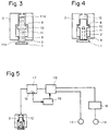
- Fig. 3 shows details of a first apparatus for carrying out the method in accordance with the invention.
- the pick-up tool 2 has a continuous longitudinal drill hole 11 to the upper end of which vacuum can be applied to grip the semiconductor chip 1.
- the longitudinal drill hole 11 is sealed at the lower end. In doing so, as the result of the pressure differential between the lower and upper ends of the longitudinal drill hole 11, a force directed upwards is created which is sufficient to push the pick-up tool 2 to the upper limit position: In this way, the pick-up tool 2 is fixed in the upper limit position on the bondhead 3.
- the vacuum at the upper end of the longitudinal drill hole 11 is switched off.
- the force directed upwards acting on the pick-up tool 2 reduces continuously with continual reduction of the vacuum:
- the pick-up tool 2 falls downwards, the semiconductor chip 1 impacts on the adhesive 5 and compresses the adhesive 5 more and more until, after the period of time ⁇ , the bondhead 3 is raised and moved away.
- the vacuum is not completely broken down, the semiconductor chip 1 remains attached to the pick-up tool 2. Therefore, the placing of the semiconductor chip 1 on the adhesive 5 takes place in a controlled manner under the guidance of the pick-up tool 2.
- the vacuum has also broken down sufficiently so that when it is raised, the bondhead 3 leaves the semiconductor chip 1 on the adhesive 5.
- Fig. 4 shows details of a second apparatus for carrying out the method in accordance with the invention.
- the bondhead 3 comprises a chamber 12 to which compressed air or vacuum can be applied in which the upper end of the pick-up tool 2 runs on air-tight bearings.
- the pick-up tool 2 When vacuum is applied to the chamber 12, then the pick-up tool 2 is pushed into its upper limit position.
- the pick-up tool 2 When compressed air is applied to the chamber 12, then the pick-up tool 2 is pushed into its lower limit position.
- the pick-up tool 2 has a longitudinal drill hole 11 which can be connected to a vacuum source.
- the bondhead 3 is now transported to the substrate 4 (Fig. 1A) and, in a first stage, is lowered to the predetermined height H above the support 6.
- the bondhead 3 now remains at the height H.
- the vacuum in the chamber 12 is now removed so that the pick-up tool 2 lowers in relation to the bondhead 3.
- the bondhead 3 remains at height H during time ⁇ which begins at the time when the vacuum is removed and ends with the raising and moving away of the bondhead 3.
- This dwell time ⁇ of the bondhead 3 at height H determines the extent to which the semiconductor chip 1 compresses the adhesive 5, ie, which adhesive thickness is achieved.
- the vacuum in the longitudinal drill hole 11 must be removed in due time before the dwell time ⁇ elapses.
- This second embodiment has the advantage that, during the time ⁇ , the strength of the vacuum or negative pressure in the chamber 12 can be controlled according to a given pressure profile so that the lowering of the semiconductor chip 1 onto the adhesive 5 takes place with controlled speed.
- the lowering speed can be reduced in comparison to the case of the sudden removal of the vacuum.
- the second embodiment is suitable for the placing of relatively large semiconductor chips onto a substrate 4 where it is desired that the semiconductor chip 1 is pressed onto the substrate with a predetermined bond force.
- a predetermined overpressure p 2 is applied to the chamber 12.
- the overpressure p 2 and the height H 1 above the support 6 to which the bondhead 3 is lowered are selected so that the pick-up tool 2 is deflected upwards in vertical direction 7 in relation to the bondhead 3 whereby the cam 10 strikes neither at the top on stop surface 8 nor at the bottom on stop surface 9.
- the layer thickness of the adhesive 5 which results is dependent on the volume of the applied portion of adhesive and on pressure p 2 .
- Fig. 5 shows a device for controlling the pressure in the chamber 12 of the bondhead 3.
- the device has a compressed air source 13 and a vacuum source 14 which are connected by a proportional valve 15.
- the vacuum source 14 is preferably connected to the proportional valve 15 via a vacuum reservoir 16.
- the outlet of the proportional valve 15 is connected to a pressure chamber 17 the volume of which is at least ten times larger than the volume of the chamber 12 when the pick-up tool 2 is located at the lower limit position.
- a pressure sensor 18 is located in the pressure chamber 17 for measuring the pressure p prevailing inside it.
- the signal delivered by the pressure sensor 18 is fed to a control device 19 which controls the proportional valve 15 so that the pressure p in the pressure chamber 17 corresponds to a given value.
- the pressure chamber 17 is connected to the chamber 12 of the bondhead 3 so that the same pressure is set in the chamber 12 as in the pressure chamber 17.
- the longitudinal drill hole 11 of the pick-up tool 2 can be separately connected to the vacuum source 14 via a not presented switchable valve for gripping and releasing the semiconductor chip 1.
Landscapes
- Die Bonding (AREA)
- Wire Bonding (AREA)
Priority Applications (1)
| Application Number | Priority Date | Filing Date | Title |
|---|---|---|---|
| EP01118958A EP1187181A3 (de) | 2000-09-12 | 2001-08-06 | Verfahren und Vorrichtung für die Montage von Halbleiterchips |
Applications Claiming Priority (3)
| Application Number | Priority Date | Filing Date | Title |
|---|---|---|---|
| EP00810820A EP1187180A1 (de) | 2000-09-12 | 2000-09-12 | Verfahren und Vorrichtung für die Montage von Halbleiterchips |
| EP00810820 | 2000-09-12 | ||
| EP01118958A EP1187181A3 (de) | 2000-09-12 | 2001-08-06 | Verfahren und Vorrichtung für die Montage von Halbleiterchips |
Publications (2)
| Publication Number | Publication Date |
|---|---|
| EP1187181A2 true EP1187181A2 (de) | 2002-03-13 |
| EP1187181A3 EP1187181A3 (de) | 2002-04-10 |
Family
ID=26074013
Family Applications (1)
| Application Number | Title | Priority Date | Filing Date |
|---|---|---|---|
| EP01118958A Withdrawn EP1187181A3 (de) | 2000-09-12 | 2001-08-06 | Verfahren und Vorrichtung für die Montage von Halbleiterchips |
Country Status (1)
| Country | Link |
|---|---|
| EP (1) | EP1187181A3 (de) |
Cited By (4)
| Publication number | Priority date | Publication date | Assignee | Title |
|---|---|---|---|---|
| WO2002095815A3 (en) * | 2001-05-22 | 2003-03-13 | Rf Micro Devices Inc | Time-based semiconductor material attachment |
| EP1424722A1 (de) * | 2002-11-29 | 2004-06-02 | Esec Trading S.A. | Verfahren zum Aufnehmen von Halbleiterchips von einer Folie und Vorrichtung |
| US6769469B2 (en) * | 1999-08-09 | 2004-08-03 | Sony Chemicals Corp. | Process for mounting semiconductor device and mounting apparatus |
| WO2026017271A1 (en) * | 2024-07-19 | 2026-01-22 | Nexperia B.V. | A method for mounting an electronics component at a particular placement location on a carrier as well as a pick-and-place apparatus for mounting an electronics component at a particular placement location on a carrier. |
Family Cites Families (3)
| Publication number | Priority date | Publication date | Assignee | Title |
|---|---|---|---|---|
| JP2635889B2 (ja) * | 1992-06-24 | 1997-07-30 | 株式会社東芝 | ダイボンディング装置 |
| JPH10340931A (ja) * | 1997-06-05 | 1998-12-22 | Toray Eng Co Ltd | チップボンディングツール |
| JP3132496B2 (ja) * | 1999-01-25 | 2001-02-05 | 松下電器産業株式会社 | ダイボンディング装置 |
-
2001
- 2001-08-06 EP EP01118958A patent/EP1187181A3/de not_active Withdrawn
Cited By (4)
| Publication number | Priority date | Publication date | Assignee | Title |
|---|---|---|---|---|
| US6769469B2 (en) * | 1999-08-09 | 2004-08-03 | Sony Chemicals Corp. | Process for mounting semiconductor device and mounting apparatus |
| WO2002095815A3 (en) * | 2001-05-22 | 2003-03-13 | Rf Micro Devices Inc | Time-based semiconductor material attachment |
| EP1424722A1 (de) * | 2002-11-29 | 2004-06-02 | Esec Trading S.A. | Verfahren zum Aufnehmen von Halbleiterchips von einer Folie und Vorrichtung |
| WO2026017271A1 (en) * | 2024-07-19 | 2026-01-22 | Nexperia B.V. | A method for mounting an electronics component at a particular placement location on a carrier as well as a pick-and-place apparatus for mounting an electronics component at a particular placement location on a carrier. |
Also Published As
| Publication number | Publication date |
|---|---|
| EP1187181A3 (de) | 2002-04-10 |
Similar Documents
| Publication | Publication Date | Title |
|---|---|---|
| US6648215B2 (en) | Method and apparatus for mounting semiconductor chips | |
| JP5491748B2 (ja) | 半導体装置の製造装置および半導体装置の製造方法 | |
| JP2014123731A (ja) | 基板上に半導体チップを実装するための熱圧着ボンディング方法および装置 | |
| TW567574B (en) | Apparatus for mounting semiconductor chips | |
| US6387733B1 (en) | Time-based semiconductor material attachment | |
| EP1449810A3 (de) | Verfahren zur Herstellung eines mikroelektromechanischen Systems mit Lötkugeln | |
| US5890283A (en) | Apparatus and method for mounting electrically conductive balls | |
| EP1187181A2 (de) | Verfahren und Vorrichtung für die Montage von Halbleiterchips | |
| KR100222098B1 (ko) | 도전성 볼의 탑재방법 및 이의 장치 | |
| KR102075198B1 (ko) | 본딩장치 및 이의 제어방법 | |
| JP2002118125A (ja) | 半導体チップを装着する方法及び装置 | |
| JP3132496B2 (ja) | ダイボンディング装置 | |
| JP2004241685A (ja) | ペレット搬送装置、ペレットボンディング方法およびペレットボンディング装置 | |
| JPH09270442A (ja) | 導電性ボールの搭載装置および搭載方法 | |
| JPH07307344A (ja) | 半田ボールのボンディング装置 | |
| CN213622181U (zh) | 一种下料夹持装置及下料装置 | |
| JPH09148790A (ja) | 電子部品装着装置 | |
| JP2003197653A (ja) | 半導体チップの実装装置 | |
| JP4119598B2 (ja) | 電子部品実装装置および電子部品実装方法 | |
| KR100745421B1 (ko) | 다이본딩장치 및 이를 이용한 다이본딩방법 | |
| JP4051166B2 (ja) | ペレットボンディング方法および装置 | |
| JP3255030B2 (ja) | 導電性ボールの搭載装置および搭載方法 | |
| US7407084B2 (en) | Method for mounting a semiconductor chip onto a substrate | |
| JP3351246B2 (ja) | 導電性ボールの搭載装置 | |
| KR100505239B1 (ko) | 비지에이 패키지용 솔더볼 장착 장치 및 방법 |
Legal Events
| Date | Code | Title | Description |
|---|---|---|---|
| PUAI | Public reference made under article 153(3) epc to a published international application that has entered the european phase |
Free format text: ORIGINAL CODE: 0009012 |
|
| PUAL | Search report despatched |
Free format text: ORIGINAL CODE: 0009013 |
|
| AK | Designated contracting states |
Kind code of ref document: A2 Designated state(s): AT BE CH CY DE DK ES FI FR GB GR IE IT LI LU MC NL PT SE TR |
|
| AX | Request for extension of the european patent |
Free format text: AL;LT;LV;MK;RO;SI |
|
| AK | Designated contracting states |
Kind code of ref document: A3 Designated state(s): AT BE CH CY DE DK ES FI FR GB GR IE IT LI LU MC NL PT SE TR |
|
| AX | Request for extension of the european patent |
Free format text: AL;LT;LV;MK;RO;SI |
|
| STAA | Information on the status of an ep patent application or granted ep patent |
Free format text: STATUS: THE APPLICATION HAS BEEN WITHDRAWN |
|
| 18W | Application withdrawn |
Withdrawal date: 20020412 |