EP1189426A2 - Plattengerät - Google Patents
Plattengerät Download PDFInfo
- Publication number
- EP1189426A2 EP1189426A2 EP01122120A EP01122120A EP1189426A2 EP 1189426 A2 EP1189426 A2 EP 1189426A2 EP 01122120 A EP01122120 A EP 01122120A EP 01122120 A EP01122120 A EP 01122120A EP 1189426 A2 EP1189426 A2 EP 1189426A2
- Authority
- EP
- European Patent Office
- Prior art keywords
- disk
- state
- power
- vacant capacity
- changing
- Prior art date
- Legal status (The legal status is an assumption and is not a legal conclusion. Google has not performed a legal analysis and makes no representation as to the accuracy of the status listed.)
- Withdrawn
Links
- 238000000034 method Methods 0.000 claims description 43
- 239000004065 semiconductor Substances 0.000 claims description 20
- 230000004044 response Effects 0.000 claims description 7
- 230000003213 activating effect Effects 0.000 claims description 3
- 230000003287 optical effect Effects 0.000 abstract description 7
- 230000008569 process Effects 0.000 description 41
- 230000006835 compression Effects 0.000 description 18
- 238000007906 compression Methods 0.000 description 18
- 238000001514 detection method Methods 0.000 description 5
- 239000002131 composite material Substances 0.000 description 2
- 238000001454 recorded image Methods 0.000 description 2
- 230000009467 reduction Effects 0.000 description 2
- 230000008859 change Effects 0.000 description 1
- 238000006243 chemical reaction Methods 0.000 description 1
- 238000010586 diagram Methods 0.000 description 1
- 230000005611 electricity Effects 0.000 description 1
- 238000000926 separation method Methods 0.000 description 1
Images
Classifications
-
- G—PHYSICS
- G11—INFORMATION STORAGE
- G11B—INFORMATION STORAGE BASED ON RELATIVE MOVEMENT BETWEEN RECORD CARRIER AND TRANSDUCER
- G11B31/00—Arrangements for the associated working of recording or reproducing apparatus with related apparatus
-
- H—ELECTRICITY
- H04—ELECTRIC COMMUNICATION TECHNIQUE
- H04N—PICTORIAL COMMUNICATION, e.g. TELEVISION
- H04N1/00—Scanning, transmission or reproduction of documents or the like, e.g. facsimile transmission; Details thereof
- H04N1/00885—Power supply means, e.g. arrangements for the control of power supply to the apparatus or components thereof
- H04N1/00888—Control thereof
- H04N1/00891—Switching on or off, e.g. for saving power when not in use
-
- H—ELECTRICITY
- H04—ELECTRIC COMMUNICATION TECHNIQUE
- H04N—PICTORIAL COMMUNICATION, e.g. TELEVISION
- H04N1/00—Scanning, transmission or reproduction of documents or the like, e.g. facsimile transmission; Details thereof
- H04N1/21—Intermediate information storage
- H04N1/2104—Intermediate information storage for one or a few pictures
- H04N1/2112—Intermediate information storage for one or a few pictures using still video cameras
-
- H—ELECTRICITY
- H04—ELECTRIC COMMUNICATION TECHNIQUE
- H04N—PICTORIAL COMMUNICATION, e.g. TELEVISION
- H04N1/00—Scanning, transmission or reproduction of documents or the like, e.g. facsimile transmission; Details thereof
- H04N1/21—Intermediate information storage
- H04N1/2104—Intermediate information storage for one or a few pictures
- H04N1/2158—Intermediate information storage for one or a few pictures using a detachable storage unit
-
- H—ELECTRICITY
- H04—ELECTRIC COMMUNICATION TECHNIQUE
- H04N—PICTORIAL COMMUNICATION, e.g. TELEVISION
- H04N5/00—Details of television systems
- H04N5/76—Television signal recording
- H04N5/765—Interface circuits between an apparatus for recording and another apparatus
- H04N5/77—Interface circuits between an apparatus for recording and another apparatus between a recording apparatus and a television camera
- H04N5/772—Interface circuits between an apparatus for recording and another apparatus between a recording apparatus and a television camera the recording apparatus and the television camera being placed in the same enclosure
-
- H—ELECTRICITY
- H04—ELECTRIC COMMUNICATION TECHNIQUE
- H04N—PICTORIAL COMMUNICATION, e.g. TELEVISION
- H04N1/00—Scanning, transmission or reproduction of documents or the like, e.g. facsimile transmission; Details thereof
- H04N1/00885—Power supply means, e.g. arrangements for the control of power supply to the apparatus or components thereof
-
- H—ELECTRICITY
- H04—ELECTRIC COMMUNICATION TECHNIQUE
- H04N—PICTORIAL COMMUNICATION, e.g. TELEVISION
- H04N2101/00—Still video cameras
-
- H—ELECTRICITY
- H04—ELECTRIC COMMUNICATION TECHNIQUE
- H04N—PICTORIAL COMMUNICATION, e.g. TELEVISION
- H04N2201/00—Indexing scheme relating to scanning, transmission or reproduction of documents or the like, and to details thereof
- H04N2201/21—Intermediate information storage
- H04N2201/214—Checking or indicating the storage space
-
- H—ELECTRICITY
- H04—ELECTRIC COMMUNICATION TECHNIQUE
- H04N—PICTORIAL COMMUNICATION, e.g. TELEVISION
- H04N5/00—Details of television systems
- H04N5/76—Television signal recording
- H04N5/84—Television signal recording using optical recording
- H04N5/85—Television signal recording using optical recording on discs or drums
-
- H—ELECTRICITY
- H04—ELECTRIC COMMUNICATION TECHNIQUE
- H04N—PICTORIAL COMMUNICATION, e.g. TELEVISION
- H04N9/00—Details of colour television systems
- H04N9/79—Processing of colour television signals in connection with recording
- H04N9/80—Transformation of the television signal for recording, e.g. modulation, frequency changing; Inverse transformation for playback
- H04N9/804—Transformation of the television signal for recording, e.g. modulation, frequency changing; Inverse transformation for playback involving pulse code modulation of the colour picture signal components
- H04N9/8042—Transformation of the television signal for recording, e.g. modulation, frequency changing; Inverse transformation for playback involving pulse code modulation of the colour picture signal components involving data reduction
- H04N9/8047—Transformation of the television signal for recording, e.g. modulation, frequency changing; Inverse transformation for playback involving pulse code modulation of the colour picture signal components involving data reduction using transform coding
Definitions
- the present invention relates to a disk apparatus. More specifically, the present invention relates to a disk apparatus which is applied to a digital camera, for example, and records a desired signal on the disk recording medium removably attached to the digital camera by exposing a laser beam to the disk recording medium.
- FAT information disk information
- the FAT information was reproduced from the recording medium in response to a power supply, and then a capturing control of the object was performed on the basis of vacant capacity information included in the reproduced FAT information. That is, in order to validate a shutter button operation, first, it is needed to confirm that the number of images capable of capturing is greater than one by detecting a vacant capacity. In the prior art, the FAT information was reproduced from the recording medium in response to the power supply.
- a primary object of the present invention is to provide a novel disk apparatus.
- Another object of the present invention is to provide a disk apparatus capable of promptly determining whether or not to fetch a desired signal.
- a disk device which records a desired signal in a disk recording medium, comprises: an attaching means for detachably attaching the disk recording means; a first changing means for changing to a power-on state when the disk recording means is attached in a power-off state; a detecting means for detecting vacant capacity information showing a vacant capacity of the disk recording means from the disk recording means when changing to the power-on state by the first changing means; a saving means for saving the vacant capacity information detected by the detecting means in a semiconductor memory; and a controlling means for controlling a fetching of the desired signal on the basis of the vacant capacity information saved in the semiconductor memory.
- the power-off-state is changed to the power-on state by the first changing means.
- the detecting means detects the vacant capacity information showing a vacant capacity of the disk recording means from the disk recording means when changing to the power-on state by the first change means.
- the detected vacant capacity information is saved in the semiconductor memory by the saving means.
- a fetching of the desired signal is controlled by the controlling means on the basis of the vacant capacity information saved in the semiconductor memory.
- the power-off-state is changed to the power-on state by the second changing means.
- the controlling means is activated by an activating means when changed to the power-on state by the second changing means. That is, a detect/save of the vacant capacity information is performed in response to the attaching of the disk recording means. In contrast, the control of the desired signal fetching is performed in response to the power supply instruction.
- the controlling means when a fetching instruction is applied, the desired signal is fetched by the fetching means. Furthermore, the controlling means includes an invalidating means for invalidating the fetching instruction on the basis of the vacant capacity information. In a case of an image signal in which maximum size of the desired signal is determined in advance, the invalidating means invalidates the fetching instruction when the vacant capacity shown by the vacant capacity information is less than the maximum size.
- the power-on state is changed to the power-off state by a third changing means. Due to this, an amount of consumed electricity is curbed.
- the semiconductor memory is preferably non-volatile.
- a recording method which records the desired signal in the detachable disk recording means comprises steps of :(a) changing to a power-on state when the disk recording means is attached in the power-off state; (b) detecting the vacant capacity information showing a vacant capacity of the disk recording means when changing to the power-on state in the step(a); (c) saving the vacant capacity information detected in the step (b) in the semiconductor memory; and (d) controlling a fetching of the desired signal on the basis of the vacant capacity information saved in the semiconductor memory.
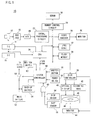
- a digital camera 10 in this embodiment includes a battery 52.
- the battery 52 recharges a back-up power source 54, and a system controller 50 is uninterruptedly rendered on-state by the back-up power source 54.
- the system controller 50 When an operator turns on a power switch 58, the system controller 50 turns on a switch SW1 and applies to a CPU 34 a state signal indicating that the power switch 58 is on-state. If the operator converts the power switch 58 from on-state to off-state, the system controller 50 outputs a corresponding state signal to the CPU 34, and then turns off the switch SW1 after a predetermined time lapse.
- the system controller 50 turns on the switch SW1, and outputs to the CPU 34 a state signal indicating that the output level of the AND gate 62 is high-level.
- a disk censor 64 outputs a high-level signal when a detachable magnetooptical disk 46 is set to a slot 48, and a slot censor 66 outputs a high-level signal when the slot 48 changes from open-state to close-state.
- the AND gate 62 subjects the outputs of the disk censor 64 and the slot censor 66 to the AND processing, when the magnetooptical disk 46 is attached, in other words when the magnetooptical disk 46 is set to the slot 48 and the slot 48 changes to close-state, a state signal indicating that the output of the AND gate 62 is high-level is applied to the CPU 34. If a detection completion notice is applied from the CPU 34 after such the state signal is outputted, the system controller 50 returns the switch SW1 to off-state.
- system controller 50 outputs to the CPU 34 a state signal indicating on/off-state of a monitor switch 60 when the monitor switch 60 is converted. Furthermore, when a shutter button 56 is operated, the system controller 50 outputs to the CPU 34 a state signal indicating the shutter button 56 is on-state.
- the CPU 34 When the state signal indicates that the output of the AND gate 62 is updated from low-level to high-level is applied, the CPU 34 outputs an initializing instruction 1 to the disk controller 38.
- the disk controller 38 rotates the magnetooptical disk 46 by the spindle motor 44, and drives an optical pick-up 40 and a recording head 42, so as to subject the magnetooptical disk 46 to a test write and a test read.
- the test write and the test read are repeatedly carried out by a different laser beam power, therefore, an optimum laser beam power value is specified.
- the disk controller 38 informs the CPU 34 that the initialization is complete.
- the CPU 34 requests the disk controller 38 for the optimum laser beam power value and the disk information (vacant capacity information of the magnetooptical disk 46, a maximum file number of the recorded image files, and etc.).
- the disk controller 38 sends back to the CPU 34 the optimal laser beam power value specified by the above described test write and the test read and the disk information read from an FAT (File Allocation Table) area of the magnetooptical disk 46.
- the CPU 34 records the sent back optimal laser beam power value and the disk information in a flash memory 36.
- the CPU 34 outputs a detection completion notice to the system controller 50. As described above, the system controller 50 turns off the switch SW1 responding to the detection completion notice.
- the CPU 34 When a state signal indicating that the power switch 58 is turned on is applied, the CPU 34 reads the disk information from the flash memory 36, and performs a configuration setting for photographing on the basis of the read disk information.
- the disk information includes the vacant capacity information of the magnetooptical disk 46 and the maximum file number of the recorded image files, etc.
- the CPU 34 calculates the number of images capable of photographing on the basis of the vacant capacity information, and determines the file number of a still image file created next time on the basis of the maximum file number.
- the CPU 34 reads the optimal laser beam power value from the flash memory 36, and applies the read optimal laser beam power value and an initializing instruction 2 to the disk controller 38.
- the disk controller 38 subjects the magnetooptical disk 46 to a simple test write and test read on the basis of the optimal laser beam power value. That is, it is determined whether or not a recording process appropriately performs by the applied optimal laser beam power value. Subsequently, if the appropriate recording process is possible, the supplied optimal laser beam power value is determined as an optimal laser beam power value of the currently attached magnetooptical disk 46.
- an optimal laser beam power value is determined by carrying out a strict test write and a test read, that is, a plurality of test writes and test reads by different laser beam powers.
- the optimal laser beam power value is determined in this manner, the initializing completion notice is outputted to the CPU 34.
- the CPU 34 When a state signal indicating the monitor switch 60 is turned on is applied, the CPU 34 performs a through image display process. More specifically, the CPU 34 outputs a thinning-out read command to a timing generator (TG) 14, and in addition outputs a predetermined process command to a signal processing circuit 22 and a video encoder 28.
- TG timing generator
- the timing generator (TG) 14 drives a CCD imager 12 in accordance with a thinning-out read scheme on the basis of a vertical synchronization signal and a horizontal synchronization signal outputted from a single generator (SG) 16. Due to this, a low-resolution camera signal (pixel signal) corresponding to an object image is outputted from the CCD imager 12. The outputted camera signal is subjected to a well-known noise reduction and a level control in a CDS/AGC circuit 18, and subsequently converted to a digital signal by an A/D converter 20.
- the signal processing circuit 22 subjects a camera data applied through the A/D converter 20 to a color separation, a white balance control, a YUV conversion and so on so as to generate a YUV data corresponding to the object image, and outputs the generated YUV data and a write request to the memory control circuit 24.
- the YUV data outputted from the signal processing circuit 22 is written in an SDRAM 26 by the memory control circuit 24.
- the video encoder 28 requests the memory control circuit 24 to read out the YUV data, and converts the YUV data read by the memory control circuit 24 into a composite video signal in accordance with an NTSC scheme.
- the converted composite video signal is applied to the monitor 30.
- a real-time moving image of the object i.e. a through image is displayed on the monitor 30.
- the CPU 34 When a state signal indicating the monitor switch 60 is turned off is applied, the CPU 34 outputs a cancel command of the thinning-out read to the TG 14, and also outputs a process cancel command to the signal processing circuit 22 and to the video encoder 28. Due to this, a through image display is cancelled.
- the CPU 34 determines the number of images capable of photographing, and validates an operation of the shutter button 56 only when it is possible to take more than one picture. In other words, responding to the applied state signal, the CPU 34 requests the TG 14 to read the entire pixels, outputs to the signal processing circuit 22 the same process command as above and outputs a compression command to a JPEG CODEC 32.
- the TG 14 drives the CCD imager 12 during a one-frame period in accordance with an entire pixel read scheme on the basis of the vertical synchronization signal and the horizontal synchronization signal.
- a high-resolution camera signal corresponding to the object image is outputted from the CCD imager 12.
- the outputted one-frame camera signal is subjected to the same process as above, and a high-resolution YUV data is outputted from the signal processing circuit 22.
- the outputted YUV data is written into the SDRAM 26 by the memory control circuit 24.
- the JPEG CODEC 32 requests the memory control circuit 24 to read the YUV data.
- the memory control circuit 24 reads the high-resolution YUV data from the SDRAM 26 corresponding to the read request, and the JPEG CODEC 32 subjects the read YUV data to a JPEG compression. Due to this, a compression still image data compressed not exceeding a maximum size of 20 K bytes is generated.
- the JPEG CODEC 32 applies the generated compression still image data and a write request to the memory control circuit 24. Due to this, the compression still image data is also stored in the SDRAM 26 by the memory control circuit 24.
- the CPU 34 requests by itself the memory control circuit 24 to read the compression still image data, and applies the read compression still image data to the disk controller 38.
- the CPU 34 also generates a file name including the file number determined when the power switch 58 is turned on, and applies the generated file name to the disk controller 38 following the compression still image data.
- the disk controller 38 drives the optical pick-up 40 and the recording head 42, and records the still image file including the compression still image data and the file name to the magnetooptical disk 46 in accordance with the FAT scheme.
- the CPU 34 When a state signal indicating the power switch 58 is turned off, the CPU 34 requests the optimal laser beam power value and the disk information to the disk controller 38. At this time, the disk controller 38 sends back to the CPU 34 the optimal laser beam power value determined by the test read and the test write based on the initializing instruction 2 and the current disk information. The CPU 34 records the sent back optimal laser beam power value and the disk information in the flash memory 36.
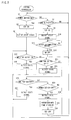
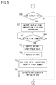
- the system controller 50 processes flowchart shown in Figure 2. First it is determined whether or not the power switch 58 is turned on in a step S1. When the power switch 58 is changed from off-state to on-state, the switch SW1 is turned on in a step S3, and a state signal indicating that the power switch 58 is turned on is outputted to the CPU 34 in a step S5.
- a state of the monitor switch 60 is determined in respective steps of S 17 and S 21.
- YES is determined in the step S17, and a state signal indicating that the monitor switch 60 has moved to on-state is outputted to the CPU 34 in a step S19.
- YES is determined in the step S21, and a state signal indicating that the monitor switch 60 has moved to off-state is outputted to the CPU 34 in a step S23.
- step S17 or S21 it is determined whether or not the shutter button 56 is operated in a step S25, and it is determined whether or not the power switch 58 is turned off in a step S29. If the shutter button 56 is operated, the process proceeds from the step S25 to a step S27, a state signal indicating that the shutter button 56 is operated is outputted to the CPU 34. In the meanwhile, if the power switch 58 is changed from on-state to off-state, the process proceeds from the step S29 to a step S31, and a state signal indicating that the power switch 58 is turned off is outputted to the CPU 34.
- step S33 After a lapse of a predetermined time period of stand-by in a step S33, the switch SW1 is turned off in a step S35. If the process of the step S 27 is complete or NO is determined in either the step S25 or the step S29, the process returns to the step S17. When a process of the step S35 is complete, the process returns to the step S1.
- step S7 If an output of the AND gate 62 changes from low-level to high-level when the power switch 58 is off-state, No is determined in the step S1, and YES is determined in a step S7.
- the switch SW1 is then turned on in a step S9, and a state signal indicating that the output of the AND gate 62 is high level is outputted to the CPU 34 in a step S11. It is determined whether or not the detection completion notice is sent back from the CPU 34 in a step S13, and if YES, the switch SW1 is turned off in a step S15. When the process of the step S15 is complete, the process returns to the step S1.
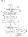
- the CPU 34 processes flowcharts shown in Figure 3 to Figure 5.
- a photographing configuration setting (a calculation of the number of images capable of photographing, a determination of a file number of still image files to be created next time, etc.) is carried out on the basis of the read disk information in a step S45, the read optimal laser beam power value and the initializing instruction 2 are outputted to the disk controller 38 in a following step S47.
- the optimal laser beam power value of the currently attached magnetooptical disk 34 is determined by the initializing instruction 2.
- step S49 It is determined whether or not the monitor switch 60 is turned on in a step S49, and it is determined whether or not the monitor switch 60 is turned off in a step S53. These determinations are also made on the basis of the state signal from the system controller 50 in a same manner as described in the step S41. If YES in the step S49, a through image display process is carried out in a step S51. More specifically, a thinning-out read command is applied to the TG 14, and a predetermined process command is applied to the signal processing circuit 22 and the video encoder 28. As a result, the through image is displayed on the monitor 30. On the other hand, if YES in the step S53, the through image display is cancelled in a step S55. More specifically, TG 14, the signal processing circuit 22 and the video encoder 28 are disabled. When processes of the steps S51 and S55 are complete, the process returns to the step S49.
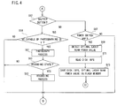
- a step S57 shown in Figure 4 it is determined whether or not the shutter button 56 is operated on the basis of the state signal from the system controller 50.
- YES it is determined whether or not the number of images capable of photographing is greater than "one" in a step S59. If NO, the process returns to the step S49 without going through processes of steps S61 to S65. Due to this, the operation of the shutter button 56 is invalidated.
- a still image photographing process is performed in the step S61. More specifically, a command of an entire pixel reading a one frame period is applied to the TG 14, a predetermined process command is applied to the signal processing circuit 22, and then a compression command is applied to the JPEG CODEC 32. Furthermore, the number of images capable of photographing and the file numbers are updated. A one-frame compression still image data is obtained in the SDRAM 26secured by the photographing process.
- the recording-capable state is a state that the optimal laser beam power is set to the optical pick-up 40, and the spindle motor 44 rotates at a predetermined speed.
- the recording-capable state is obtained when the initializing completion notice is sent back from the disk controller 38 responding to the above initializing instruction 2, or when a rotation of the spindle motor 44 is resumed for a recording process from the state that the rotation of the spindle motor 44 is provisionally interrupted for a reduction in electric power consumption.
- the process returns from the step S63 to the step S49. However, if the recording-capable state is obtained, the process returns to the step S49 after performing a recording process in the step S65.
- the compression still image data is read from the SDRAM 26 through the memory control circuit 24, and the read compression still image data and a file name voluntarily generated are applied to the disk controller 38.
- the still image file including the compression still image data and the file name is recorded in the magnetooptical disk 46 by the optical pick-up 40 and the recording head 42.
- a step S67 it is determined whether or not the power switch 58 is turned off on the basis of the state signal from the system controller 50.
- the optimal laser beam power value and the disk information are detected through the disk controller 38 in respective steps S69 and S71. More specifically, the optimal laser beam power value determined in the disk controller 38 on the basis of the above initializing instruction 2 is detected in the step S69, and the current disk information is read in the step S71.
- the optimal laser beam power value and the disk information thus obtained are stored in the flash memory 36, and the process returns to step S41 upon completing a process of the step S73.
- step S41 If NO is determined in the step S41, the process proceeds to a step S75 shown in Figure 5, it is determined whether or not the output of the AND gate 62 changes from low-level to high-level. This determination is also made on the basis of the state signal from the system controller 50.
- the initializing instruction 1 is applied to the disk controller 38 in a step S77. By the initializing instruction 1, the test read and test write are repeatedly performed by different laser beam powers, and the optimal laser beam power value is determined.
- step S79 When the initializing completion notice is issued from the disk controller 38 after the optimal laser beam power value is determined, YES is determined in a step S79, and the optimal laser beam power value and the disk information are detected through the disk controller 38 in respective steps S81 and S83. That is, the optimal laser beam power value determined on the basis of the initializing instruction 1 is detected in the step S81, and the current disk information is read from the magnetooptical disk 46 in the step S83. The optimal laser beam power value and the disk information thus obtained are stored in the flash memory 36 in a step S85, and the detection completion notice is outputted to the system controller 50 in a following step S87. Upon completing the step S87, the process returns to the step S41.
- the digital camera 10 is driven by a battery power, and records the still image file by the optical pick-up 40 and the recording head 42 in the magnetooptical disk 46 rotated by the spindle motor 44.
- the magnetooptical disk 46 is detachably attached by the slot 48.
- the magnetooptical disk 46 is attached to the slot 48 while the battery 52 is off-state the battery 52 is turned on by the system controller 50.
- the CPU 34 reads the disk information including the vacant capacity information of the magnetooptical disk 46 after the battery 52 is turned on, and saves the read disk information in the flash memory 36. Upon completion of saving the disk information, the battery 52 is turned off by the system controller 50.
- the CPU 34 When the power switch 58 is turned on, the CPU 34 reads the vacant capacity information from the flash memory 36, and calculates the number of images capable of photographing on the basis of the vacant capacity information. Only when the number of images capable of photographing is greater than "one", the still image photographing process of the object and the recording process of the still image file to the magnetooptical disk 46 is carried out in response to the operation of the shutter button 56. In other words, when the number of images capable of photographing is "0", the operation of the shutter button 56 is invalidated.
- the vacant capacity information is thus saved in the semiconductor memory having a faster access capability compared to that of a disk recording medium, it is possible to promptly determine whether or not the shutter button operation should be rendered validated when the battery power is applied
- the disk information is saved in the flash memory 36 incorporated in the digital camera 10 in this embodiment.
- the semiconductor memory saving the disk information is provided in the disk recording medium.
- the magnetooptical disk is used as the disk recording medium in this embodiment.
- a detachable hard disk such as a Micro Drive provided by IBM Corporation may be used instead of the magnetooptical disk 46.
- a non-volatile flash memory is used as a semiconductor memory to save the disk information in this embodiment.
- the disk information may also be saved in a volatile semiconductor memory constantly backed-up by a back-up power source.
- the FAT scheme is used as a recording scheme to record the still image file in the magnetooptical disk 46 in this embodiment.
- a UDF (Universal Disc Format) scheme may instead be used.
- CMOS imager is used to photograph an object in this embodiment
- CMOS imager may instead be used.
- the disk device of the present invention may be adapted to a standing-type disk recorder
Landscapes
- Engineering & Computer Science (AREA)
- Multimedia (AREA)
- Signal Processing (AREA)
- Studio Devices (AREA)
- Optical Recording Or Reproduction (AREA)
- Indexing, Searching, Synchronizing, And The Amount Of Synchronization Travel Of Record Carriers (AREA)
- Television Signal Processing For Recording (AREA)
Applications Claiming Priority (2)
| Application Number | Priority Date | Filing Date | Title |
|---|---|---|---|
| JP2000281219A JP2002093023A (ja) | 2000-09-18 | 2000-09-18 | ディスク装置 |
| JP2000281219 | 2000-09-18 |
Publications (2)
| Publication Number | Publication Date |
|---|---|
| EP1189426A2 true EP1189426A2 (de) | 2002-03-20 |
| EP1189426A3 EP1189426A3 (de) | 2004-09-15 |
Family
ID=18765908
Family Applications (1)
| Application Number | Title | Priority Date | Filing Date |
|---|---|---|---|
| EP01122120A Withdrawn EP1189426A3 (de) | 2000-09-18 | 2001-09-14 | Plattengerät |
Country Status (6)
| Country | Link |
|---|---|
| US (1) | US7123554B2 (de) |
| EP (1) | EP1189426A3 (de) |
| JP (1) | JP2002093023A (de) |
| KR (1) | KR100400707B1 (de) |
| CN (1) | CN1214627C (de) |
| TW (1) | TW514902B (de) |
Families Citing this family (6)
| Publication number | Priority date | Publication date | Assignee | Title |
|---|---|---|---|---|
| JP2003303472A (ja) * | 2002-04-04 | 2003-10-24 | Hitachi Ltd | 情報記録装置及び情報記録方法 |
| JP3794345B2 (ja) | 2002-04-25 | 2006-07-05 | 株式会社日立製作所 | 情報記録装置及び情報記録方法 |
| TWI234066B (en) * | 2003-04-15 | 2005-06-11 | Micro Star Int Co Ltd | Control circuit of optical recording medium device and method thereof |
| JP2006120304A (ja) * | 2004-09-21 | 2006-05-11 | Canon Inc | データ処理装置及びその制御方法及びプログラム及び記憶媒体 |
| JP4577388B2 (ja) * | 2008-03-31 | 2010-11-10 | 株式会社日立製作所 | 記録または再生装置 |
| JP4569662B2 (ja) * | 2008-04-24 | 2010-10-27 | 株式会社日立製作所 | 情報記録装置及び情報記録方法 |
Family Cites Families (19)
| Publication number | Priority date | Publication date | Assignee | Title |
|---|---|---|---|---|
| JPS54136241A (en) | 1978-04-14 | 1979-10-23 | Canon Inc | Electronic unit |
| JPS5971102A (ja) | 1982-10-15 | 1984-04-21 | Canon Inc | 記録又は再生装置 |
| JPS62172560A (ja) | 1986-01-23 | 1987-07-29 | Fuji Photo Film Co Ltd | 電子スチル・カメラ |
| JPS62170066A (ja) | 1986-01-23 | 1987-07-27 | Fuji Photo Film Co Ltd | 電子スチル・カメラ |
| JPS62273660A (ja) | 1986-05-21 | 1987-11-27 | Canon Inc | 記録又は再生装置 |
| US4825324A (en) | 1986-08-29 | 1989-04-25 | Fuji Photo Film Co., Ltd. | Still video camera with continuous picture-taking mode |
| JPH03276457A (ja) | 1990-03-27 | 1991-12-06 | Matsushita Electric Ind Co Ltd | 書き替え形光ディスク装置 |
| JP2843103B2 (ja) | 1990-04-04 | 1999-01-06 | シャープ株式会社 | 情報記録再生装置 |
| US5268889A (en) * | 1990-06-21 | 1993-12-07 | Yamaha Corporation | Display device for a compact disc player and a compact disc |
| JPH0467468A (ja) | 1990-07-09 | 1992-03-03 | Fujitsu Ltd | ディスク装置の書込み制御方式 |
| JPH04105269A (ja) | 1990-08-24 | 1992-04-07 | Sony Corp | ディスク記録装置及びディスク記録再生装置 |
| JPH05276471A (ja) * | 1992-03-25 | 1993-10-22 | Asahi Optical Co Ltd | 電子スチルカメラの空きトラック検索装置 |
| KR0175262B1 (ko) * | 1996-02-27 | 1999-04-15 | 김광호 | 멀티디스크 플레이어의 재생기능 제어방법 |
| US5892738A (en) * | 1996-06-25 | 1999-04-06 | Sanyo Electric Co., Ltd. | Disk recording-playback device and disk loading or unloading method |
| JPH1011755A (ja) | 1996-06-27 | 1998-01-16 | Sony Corp | 記録パワー調整方法およびそれを使用したディスク装置 |
| JPH1051722A (ja) | 1996-08-05 | 1998-02-20 | Hitachi Ltd | ディスクを記録媒体とするカメラ |
| JPH11110917A (ja) | 1997-10-01 | 1999-04-23 | Matsushita Electric Ind Co Ltd | 記録装置及び記録方法 |
| JP2000066947A (ja) | 1998-08-21 | 2000-03-03 | Canon Inc | データ記録装置及びその方法 |
| DE69941584D1 (de) | 1999-08-31 | 2009-12-03 | Lucent Technologies Inc | System für einen Handover in einem zellularen Mobilfunknetz |
-
2000
- 2000-09-18 JP JP2000281219A patent/JP2002093023A/ja active Pending
-
2001
- 2001-08-27 TW TW090120997A patent/TW514902B/zh not_active IP Right Cessation
- 2001-09-14 US US09/951,524 patent/US7123554B2/en not_active Expired - Fee Related
- 2001-09-14 EP EP01122120A patent/EP1189426A3/de not_active Withdrawn
- 2001-09-18 CN CNB01133178XA patent/CN1214627C/zh not_active Expired - Fee Related
- 2001-09-18 KR KR10-2001-0057678A patent/KR100400707B1/ko not_active Expired - Fee Related
Also Published As
| Publication number | Publication date |
|---|---|
| KR20020022042A (ko) | 2002-03-23 |
| CN1214627C (zh) | 2005-08-10 |
| CN1347088A (zh) | 2002-05-01 |
| JP2002093023A (ja) | 2002-03-29 |
| EP1189426A3 (de) | 2004-09-15 |
| KR100400707B1 (ko) | 2003-10-08 |
| TW514902B (en) | 2002-12-21 |
| US7123554B2 (en) | 2006-10-17 |
| US20020034141A1 (en) | 2002-03-21 |
Similar Documents
| Publication | Publication Date | Title |
|---|---|---|
| EP1109403B1 (de) | Datenaufzeichnungsgerät | |
| EP1189426A2 (de) | Plattengerät | |
| JP2002101377A (ja) | ハイブリッドカメラ | |
| JP4298088B2 (ja) | 撮像装置及びその制御方法 | |
| JP3772768B2 (ja) | 電子機器、撮像装置および電源制御方法 | |
| JP2001186386A (ja) | 画像処理装置及びその制御方法並びに記憶媒体 | |
| JP2001223929A (ja) | ビデオカメラ | |
| JP2003244593A (ja) | ディスク装置 | |
| JP2001008142A (ja) | 電子カメラ | |
| JP2002300511A (ja) | 電子カメラ及び電子カメラの記録方法 | |
| JP2001169162A (ja) | ディジタルカメラ | |
| JP2000352758A (ja) | 電子カメラ | |
| JP2774729B2 (ja) | 撮像装置 | |
| JP2003274262A (ja) | 電子機器、撮像装置および電源制御方法 | |
| JP4289723B2 (ja) | 画像記録装置及びその制御方法並びに記憶媒体 | |
| JP3093700B2 (ja) | 電子カメラ | |
| JPH0556321A (ja) | 記録装置 | |
| JP3119397B2 (ja) | 画像信号記録装置 | |
| JP4599008B2 (ja) | 撮像装置および撮像装置の制御方法 | |
| JP2001136475A (ja) | 電子カメラ装置 | |
| JP2002330374A (ja) | デジタルカメラとその制御方法 | |
| JP2007124178A (ja) | 映像信号記録再生装置 | |
| JP2009300579A (ja) | 撮像装置およびストロボ装置の充電制御方法 | |
| JP2004077949A (ja) | カメラ | |
| JP2002100121A (ja) | 動画像記録装置 |
Legal Events
| Date | Code | Title | Description |
|---|---|---|---|
| PUAI | Public reference made under article 153(3) epc to a published international application that has entered the european phase |
Free format text: ORIGINAL CODE: 0009012 |
|
| AK | Designated contracting states |
Kind code of ref document: A2 Designated state(s): AT BE CH CY DE DK ES FI FR GB GR IE IT LI LU MC NL PT SE TR |
|
| AX | Request for extension of the european patent |
Free format text: AL;LT;LV;MK;RO;SI |
|
| PUAL | Search report despatched |
Free format text: ORIGINAL CODE: 0009013 |
|
| AK | Designated contracting states |
Kind code of ref document: A3 Designated state(s): AT BE CH CY DE DK ES FI FR GB GR IE IT LI LU MC NL PT SE TR |
|
| AX | Request for extension of the european patent |
Extension state: AL LT LV MK RO SI |
|
| 17P | Request for examination filed |
Effective date: 20040915 |
|
| 17Q | First examination report despatched |
Effective date: 20050411 |
|
| AKX | Designation fees paid |
Designated state(s): DE FR GB |
|
| 17Q | First examination report despatched |
Effective date: 20050411 |
|
| GRAP | Despatch of communication of intention to grant a patent |
Free format text: ORIGINAL CODE: EPIDOSNIGR1 |
|
| STAA | Information on the status of an ep patent application or granted ep patent |
Free format text: STATUS: THE APPLICATION HAS BEEN WITHDRAWN |
|
| 18W | Application withdrawn |
Effective date: 20110113 |