EP1201419A2 - Procédé pour fabriquer un dispositif ferroélectrique - Google Patents
Procédé pour fabriquer un dispositif ferroélectrique Download PDFInfo
- Publication number
- EP1201419A2 EP1201419A2 EP01122324A EP01122324A EP1201419A2 EP 1201419 A2 EP1201419 A2 EP 1201419A2 EP 01122324 A EP01122324 A EP 01122324A EP 01122324 A EP01122324 A EP 01122324A EP 1201419 A2 EP1201419 A2 EP 1201419A2
- Authority
- EP
- European Patent Office
- Prior art keywords
- layer
- ferroelectric
- adhesive
- substrate
- expanding
- Prior art date
- Legal status (The legal status is an assumption and is not a legal conclusion. Google has not performed a legal analysis and makes no representation as to the accuracy of the status listed.)
- Granted
Links
Images



Classifications
-
- H—ELECTRICITY
- H10—SEMICONDUCTOR DEVICES; ELECTRIC SOLID-STATE DEVICES NOT OTHERWISE PROVIDED FOR
- H10N—ELECTRIC SOLID-STATE DEVICES NOT OTHERWISE PROVIDED FOR
- H10N30/00—Piezoelectric or electrostrictive devices
- H10N30/01—Manufacture or treatment
- H10N30/07—Forming of piezoelectric or electrostrictive parts or bodies on an electrical element or another base
- H10N30/072—Forming of piezoelectric or electrostrictive parts or bodies on an electrical element or another base by laminating or bonding of piezoelectric or electrostrictive bodies
- H10N30/073—Forming of piezoelectric or electrostrictive parts or bodies on an electrical element or another base by laminating or bonding of piezoelectric or electrostrictive bodies by fusion of metals or by adhesives
-
- B—PERFORMING OPERATIONS; TRANSPORTING
- B32—LAYERED PRODUCTS
- B32B—LAYERED PRODUCTS, i.e. PRODUCTS BUILT-UP OF STRATA OF FLAT OR NON-FLAT, e.g. CELLULAR OR HONEYCOMB, FORM
- B32B7/00—Layered products characterised by the relation between layers; Layered products characterised by the relative orientation of features between layers, or by the relative values of a measurable parameter between layers, i.e. products comprising layers having different physical, chemical or physicochemical properties; Layered products characterised by the interconnection of layers
- B32B7/04—Interconnection of layers
- B32B7/12—Interconnection of layers using interposed adhesives or interposed materials with bonding properties
-
- B—PERFORMING OPERATIONS; TRANSPORTING
- B32—LAYERED PRODUCTS
- B32B—LAYERED PRODUCTS, i.e. PRODUCTS BUILT-UP OF STRATA OF FLAT OR NON-FLAT, e.g. CELLULAR OR HONEYCOMB, FORM
- B32B38/00—Ancillary operations in connection with laminating processes
- B32B38/18—Handling of layers or the laminate
- B32B38/1866—Handling of layers or the laminate conforming the layers or laminate to a convex or concave profile
-
- B—PERFORMING OPERATIONS; TRANSPORTING
- B32—LAYERED PRODUCTS
- B32B—LAYERED PRODUCTS, i.e. PRODUCTS BUILT-UP OF STRATA OF FLAT OR NON-FLAT, e.g. CELLULAR OR HONEYCOMB, FORM
- B32B7/00—Layered products characterised by the relation between layers; Layered products characterised by the relative orientation of features between layers, or by the relative values of a measurable parameter between layers, i.e. products comprising layers having different physical, chemical or physicochemical properties; Layered products characterised by the interconnection of layers
- B32B7/02—Physical, chemical or physicochemical properties
- B32B7/027—Thermal properties
-
- H—ELECTRICITY
- H10—SEMICONDUCTOR DEVICES; ELECTRIC SOLID-STATE DEVICES NOT OTHERWISE PROVIDED FOR
- H10N—ELECTRIC SOLID-STATE DEVICES NOT OTHERWISE PROVIDED FOR
- H10N30/00—Piezoelectric or electrostrictive devices
- H10N30/20—Piezoelectric or electrostrictive devices with electrical input and mechanical output, e.g. functioning as actuators or vibrators
- H10N30/204—Piezoelectric or electrostrictive devices with electrical input and mechanical output, e.g. functioning as actuators or vibrators using bending displacement, e.g. unimorph, bimorph or multimorph cantilever or membrane benders
-
- B—PERFORMING OPERATIONS; TRANSPORTING
- B32—LAYERED PRODUCTS
- B32B—LAYERED PRODUCTS, i.e. PRODUCTS BUILT-UP OF STRATA OF FLAT OR NON-FLAT, e.g. CELLULAR OR HONEYCOMB, FORM
- B32B38/00—Ancillary operations in connection with laminating processes
- B32B38/18—Handling of layers or the laminate
- B32B2038/1891—Using a robot for handling the layers
-
- B—PERFORMING OPERATIONS; TRANSPORTING
- B32—LAYERED PRODUCTS
- B32B—LAYERED PRODUCTS, i.e. PRODUCTS BUILT-UP OF STRATA OF FLAT OR NON-FLAT, e.g. CELLULAR OR HONEYCOMB, FORM
- B32B2309/00—Parameters for the laminating or treatment process; Apparatus details
- B32B2309/02—Temperature
-
- B—PERFORMING OPERATIONS; TRANSPORTING
- B32—LAYERED PRODUCTS
- B32B—LAYERED PRODUCTS, i.e. PRODUCTS BUILT-UP OF STRATA OF FLAT OR NON-FLAT, e.g. CELLULAR OR HONEYCOMB, FORM
- B32B2311/00—Metals, their alloys or their compounds
-
- B—PERFORMING OPERATIONS; TRANSPORTING
- B32—LAYERED PRODUCTS
- B32B—LAYERED PRODUCTS, i.e. PRODUCTS BUILT-UP OF STRATA OF FLAT OR NON-FLAT, e.g. CELLULAR OR HONEYCOMB, FORM
- B32B2315/00—Other materials containing non-metallic inorganic compounds not provided for in groups B32B2311/00 - B32B2313/04
- B32B2315/02—Ceramics
-
- B—PERFORMING OPERATIONS; TRANSPORTING
- B32—LAYERED PRODUCTS
- B32B—LAYERED PRODUCTS, i.e. PRODUCTS BUILT-UP OF STRATA OF FLAT OR NON-FLAT, e.g. CELLULAR OR HONEYCOMB, FORM
- B32B37/00—Methods or apparatus for laminating, e.g. by curing or by ultrasonic bonding
- B32B37/08—Methods or apparatus for laminating, e.g. by curing or by ultrasonic bonding characterised by the cooling method
Definitions
- the expansion layer 103 is designed to be flexible, expandable and electrical to be a leader. So there are ductile metals and alloys for this layer useful.
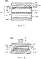
- the expansion layer 103 is preferably patterned, as in FIG 2 is shown. 2 shows schematically the different layers in partial cross-section, supported on a support member 203 and arranged between an upper plate 201 and a lower plate 202 of a hot press apparatus 200.
- the hot press apparatus 200 as further shown in FIG. 3 is described below.
- a second embodiment, according to the present invention, is a method for manufacturing a ferroelectric device 100, such as those shown in FIGS 1A and 1B is shown.
- This procedure is related to the Manufacture of a ferroelectric device described that a patterned Expanding layer 103 (like aluminum), a pre-contacted ferroelectric actuation layer 102 (such as a PZT ceramic wafer) and a substrate layer 101 (like stainless or stainless steel).
- a ferroelectric To use the actuating layer 102 which is equipped with electrodes beforehand, which is pre-contacted is the use of pre-contacted wafers for the ferroelectric Actuation layer 102 preferred.
- the ferroelectric actuation layer 102 is then rotated a second to expose (opposite) surface of the ferroelectric actuation layer 102, and a coating of liquid or solid thermoplastic Polymer adhesive or adhesive is applied to the second surface.
- the Ferroelectric actuation layer 102 is then again in the one mentioned above Way heated to evaporate the volatile components. It should be noted be that it is for the opposite surfaces of the ferroelectric Actuating layer 102 is not necessary in the manner just described one after the other to be processed.
- the ferroelectric actuation layer 102 can also be supported on their edges, for example, so that both are opposite Surfaces can be coated with adhesive or adhesive, before the ferroelectric actuation layer 102 is heated to the volatile Drive out components.
- plates 201 and 202 will be called Press 200 held at constant temperatures until the pressure from the device assembly 115 is solved.
- this procedure is not based on it limited, and it is preferable to control the temperatures of the hot press plates 201 and 202 change during bonding when using hot melt adhesives become.
- the temperatures of the plates 201 and 202 are desirable to then the temperatures of the plates 201 and 202 to values below to reduce the softening temperatures of the hot-melt adhesive in order to Adhesive or the adhesive to solidify while maintaining the pressure.
- Such cooling prevents the adhesive from flowing after it has passed through the hot Pressing applied pressure is removed.
- This movement is advantageous because it allows the deforming member 502 allows the component assembly 115 to radially outward from the center press, whereby between the expanding layer 103 and the ferroelectric Actuation layer 102 minimizes the occurrence of air bubbles that would otherwise would be trapped between those layers.
- electrical lines such. B. cables to be connected that an electrical contact to the substrate 101 or the expanding layer 103 is manufactured. If the substrate is not electrically conductive, electrical should Contact to be made to the second electrode layer 107 on of the ferroelectric actuation layer 102 is arranged.
- the lines can by conventional methods such as soldering, brazing and epoxy resin gluing be attached.
- lines that are conductive silicon or conductive Springs included are used to make electrical contact between the device and an electrical source.
- the ferroelectric device 100 includes those according to that described above Process was made to take advantage of a patterned expansion layer 103.
- this is a patterned expansion layer 103 in addition to any existing thin electrodes 106 and 107, that are already present on the ferroelectric actuation layer 102 can.
- the pattern allows the expansion layer 103, and such a patterned expansion layer 103 can be for an electrical potential on the entire ferroelectric actuation layer 102, including Areas that can break.
- the patterned expansion layer ensures 103 for a protective function that the durability of the ferroelectric device increases, and can also areas of the ferroelectric actuation layer 102 assist when breaking the ferroelectric actuation layer 102 occurs.
Landscapes
- Physics & Mathematics (AREA)
- Thermal Sciences (AREA)
- Engineering & Computer Science (AREA)
- Manufacturing & Machinery (AREA)
- Particle Formation And Scattering Control In Inkjet Printers (AREA)
- Formation Of Insulating Films (AREA)
Applications Claiming Priority (4)
| Application Number | Priority Date | Filing Date | Title |
|---|---|---|---|
| US23344200P | 2000-09-18 | 2000-09-18 | |
| US233442P | 2000-09-18 | ||
| US72262000A | 2000-11-28 | 2000-11-28 | |
| US722620 | 2000-11-28 |
Publications (3)
| Publication Number | Publication Date |
|---|---|
| EP1201419A2 true EP1201419A2 (fr) | 2002-05-02 |
| EP1201419A3 EP1201419A3 (fr) | 2003-11-26 |
| EP1201419B1 EP1201419B1 (fr) | 2007-11-07 |
Family
ID=26926927
Family Applications (1)
| Application Number | Title | Priority Date | Filing Date |
|---|---|---|---|
| EP01122324A Expired - Lifetime EP1201419B1 (fr) | 2000-09-18 | 2001-09-18 | Procédé pour fabriquer un dispositif ferroélectrique |
Country Status (2)
| Country | Link |
|---|---|
| EP (1) | EP1201419B1 (fr) |
| DE (1) | DE50113227D1 (fr) |
Cited By (4)
| Publication number | Priority date | Publication date | Assignee | Title |
|---|---|---|---|---|
| WO2005001950A1 (fr) * | 2003-02-10 | 2005-01-06 | The Boeing Company | Appareil piezoelectrique monocristallin et procede de production de cet appareil |
| FR2904788A1 (fr) * | 2006-08-11 | 2008-02-15 | Itw Gunther Sa | Plaque munie d'au moins un bord recourbe et procede de fabrication d'un telle plaque |
| NL2024798B1 (nl) * | 2020-01-30 | 2021-09-10 | Aae B V | Lijminrichting alsmede werkwijze voor het lijmen van een piëzo-element op een flowcell |
| EP3525347B1 (fr) * | 2016-10-06 | 2024-08-07 | Shin-Etsu Chemical Co., Ltd. | Procédé de fabrication d'un substrat composite |
Family Cites Families (6)
| Publication number | Priority date | Publication date | Assignee | Title |
|---|---|---|---|---|
| US5471721A (en) * | 1993-02-23 | 1995-12-05 | Research Corporation Technologies, Inc. | Method for making monolithic prestressed ceramic devices |
| JP2998503B2 (ja) * | 1993-08-05 | 2000-01-11 | 株式会社村田製作所 | 積層セラミック電子部品の製造方法 |
| US5741883A (en) * | 1994-12-16 | 1998-04-21 | The United States Of America As Represented By The Administrator Of The National Aeronautics And Space Administration | Tough, soluble, aromatic, thermoplastic copolyimides |
| US5632841A (en) * | 1995-04-04 | 1997-05-27 | The United States Of America As Represented By The Administrator Of The National Aeronautics And Space Administration | Thin layer composite unimorph ferroelectric driver and sensor |
| JPH10208319A (ja) * | 1997-01-28 | 1998-08-07 | Kitano Eng Kk | ディスク基板の貼り合わせ方法 |
| US6030480A (en) * | 1997-07-25 | 2000-02-29 | Face International Corp. | Method for manufacturing multi-layered high-deformation piezoelectric actuators and sensors |
-
2001
- 2001-09-18 EP EP01122324A patent/EP1201419B1/fr not_active Expired - Lifetime
- 2001-09-18 DE DE50113227T patent/DE50113227D1/de not_active Expired - Lifetime
Cited By (6)
| Publication number | Priority date | Publication date | Assignee | Title |
|---|---|---|---|---|
| WO2005001950A1 (fr) * | 2003-02-10 | 2005-01-06 | The Boeing Company | Appareil piezoelectrique monocristallin et procede de production de cet appareil |
| US6994762B2 (en) | 2003-02-10 | 2006-02-07 | The Boeing Company | Single crystal piezo (SCP) apparatus and method of forming same |
| FR2904788A1 (fr) * | 2006-08-11 | 2008-02-15 | Itw Gunther Sa | Plaque munie d'au moins un bord recourbe et procede de fabrication d'un telle plaque |
| WO2008020120A1 (fr) * | 2006-08-11 | 2008-02-21 | Itw Gunther | Plaque munie d'au moins un bord recourbé et procédé de fabrication d'une telle plaque |
| EP3525347B1 (fr) * | 2016-10-06 | 2024-08-07 | Shin-Etsu Chemical Co., Ltd. | Procédé de fabrication d'un substrat composite |
| NL2024798B1 (nl) * | 2020-01-30 | 2021-09-10 | Aae B V | Lijminrichting alsmede werkwijze voor het lijmen van een piëzo-element op een flowcell |
Also Published As
| Publication number | Publication date |
|---|---|
| DE50113227D1 (de) | 2007-12-20 |
| EP1201419A3 (fr) | 2003-11-26 |
| EP1201419B1 (fr) | 2007-11-07 |
Similar Documents
| Publication | Publication Date | Title |
|---|---|---|
| DE69629283T2 (de) | Ferroelektrischer dünnlagiger monomorpher verbundsensor und verfahren zu seiner herstellung | |
| DE69304443T2 (de) | Verfahren zur Herstellung einer piezoelektrischen drucksensitiven Taste oder Tastatur und durch dieses Verfahren erhaltenes Produkt | |
| DE69735416T2 (de) | Herstellung von elektroden für piezokeramische wandler | |
| EP0958620B1 (fr) | Actionneur piezo-electrique avec mise en contact d'un type nouveau et procede de fabrication dudit actionneur | |
| EP2382656B1 (fr) | Procédé de séparation pour système stratifié comprenant une tranche | |
| DE69835798T2 (de) | Verfahren um dünnschichtbauelemente zu transferieren | |
| DE4107158A1 (de) | Laminarer piezoelektrischer/elektrostriktiver treiber mit longitudinaleffekt und druckaktuator mit diesem treiber | |
| DE102015100863B4 (de) | Verfahren zur Handhabung eines Produktsubstrats und ein verklebtes Substratsystem | |
| DE102007019321A1 (de) | Elektret-Kondensatormikrofon und Verfahren zum Herstellen desselben | |
| DE1807602A1 (de) | Piezoelektrische Vorrichtung und Verfahren zu ihrer Herstellung | |
| DE69010561T2 (de) | Verfahren and Apparat zum Verbinden elektrischer Bauelemente mittels Lötelementen. | |
| DE2532009A1 (de) | Verfahren zur herstellung eines elektrischen bauteiles, bestehend aus mindestens zwei durch eine isolierschicht getrennte bauelemente | |
| EP1201419B1 (fr) | Procédé pour fabriquer un dispositif ferroélectrique | |
| DE19739684B4 (de) | Verfahren zur Herstellung von Chipstapeln | |
| DE102008050798A1 (de) | Verfahren zum Positionieren und Fixieren eines Bauteils auf einem anderen Bauteil sowie eine Anordnung zum Positionieren und Vorfixieren | |
| DE69316159T2 (de) | Verfahren zum Aufbringen von Kontakthöckern auf einer Halbleitervorrichtung sowie zum Verbinden dieser Vorrichtung mit einer Leiterplatte | |
| EP1263060B1 (fr) | Méthode de fabrication d'un transducteur à flexion plat multicouche et transducteur correspondant | |
| EP2659505B1 (fr) | Appareil et procede pour attacher deux plaquettes | |
| EP3140856B1 (fr) | Procédé et dispositif de liaison permanente | |
| EP0542772A1 (fr) | Connexion d'un transducteur piezoelectrique de flexion. | |
| DE4025435C2 (de) | Piezoelektrischer Biegewandler und Verfahren zu seiner Herstellung | |
| DE60130108T2 (de) | Verfahren zur herstellung elektrischer verbindungselemente und verbindungselement | |
| EP0657024A1 (fr) | Procede de fabrication de composants miniaturises | |
| DE4302892C2 (de) | Verfahren zur Herstellung eines Tastschalters | |
| EP2019421A2 (fr) | Dispositif semi-conducteur de puissance avec couche de contact métallique et procédé de fabrication correspondant |
Legal Events
| Date | Code | Title | Description |
|---|---|---|---|
| PUAI | Public reference made under article 153(3) epc to a published international application that has entered the european phase |
Free format text: ORIGINAL CODE: 0009012 |
|
| AK | Designated contracting states |
Kind code of ref document: A2 Designated state(s): AT BE CH CY DE DK ES FI FR GB GR IE IT LI LU MC NL PT SE TR |
|
| AX | Request for extension of the european patent |
Free format text: AL;LT;LV;MK;RO;SI |
|
| PUAL | Search report despatched |
Free format text: ORIGINAL CODE: 0009013 |
|
| AK | Designated contracting states |
Kind code of ref document: A3 Designated state(s): AT BE CH CY DE DK ES FI FR GB GR IE IT LI LU MC NL PT SE TR |
|
| AX | Request for extension of the european patent |
Extension state: AL LT LV MK RO SI |
|
| RAP1 | Party data changed (applicant data changed or rights of an application transferred) |
Owner name: CATERPILLAR INC. |
|
| 17P | Request for examination filed |
Effective date: 20040525 |
|
| AKX | Designation fees paid |
Designated state(s): AT |
|
| RBV | Designated contracting states (corrected) |
Designated state(s): DE |
|
| REG | Reference to a national code |
Ref country code: DE Ref legal event code: 8566 |
|
| 17Q | First examination report despatched |
Effective date: 20040910 |
|
| GRAP | Despatch of communication of intention to grant a patent |
Free format text: ORIGINAL CODE: EPIDOSNIGR1 |
|
| GRAJ | Information related to disapproval of communication of intention to grant by the applicant or resumption of examination proceedings by the epo deleted |
Free format text: ORIGINAL CODE: EPIDOSDIGR1 |
|
| GRAP | Despatch of communication of intention to grant a patent |
Free format text: ORIGINAL CODE: EPIDOSNIGR1 |
|
| GRAS | Grant fee paid |
Free format text: ORIGINAL CODE: EPIDOSNIGR3 |
|
| GRAA | (expected) grant |
Free format text: ORIGINAL CODE: 0009210 |
|
| AK | Designated contracting states |
Kind code of ref document: B1 Designated state(s): DE |
|
| RIC1 | Information provided on ipc code assigned before grant |
Ipc: B32B 38/18 20060101AFI20070928BHEP Ipc: H01L 41/22 20060101ALI20070928BHEP |
|
| REF | Corresponds to: |
Ref document number: 50113227 Country of ref document: DE Date of ref document: 20071220 Kind code of ref document: P |
|
| PLBE | No opposition filed within time limit |
Free format text: ORIGINAL CODE: 0009261 |
|
| STAA | Information on the status of an ep patent application or granted ep patent |
Free format text: STATUS: NO OPPOSITION FILED WITHIN TIME LIMIT |
|
| 26N | No opposition filed |
Effective date: 20080808 |
|
| PGFP | Annual fee paid to national office [announced via postgrant information from national office to epo] |
Ref country code: DE Payment date: 20100930 Year of fee payment: 10 |
|
| REG | Reference to a national code |
Ref country code: DE Ref legal event code: R119 Ref document number: 50113227 Country of ref document: DE Effective date: 20120403 |
|
| PG25 | Lapsed in a contracting state [announced via postgrant information from national office to epo] |
Ref country code: DE Free format text: LAPSE BECAUSE OF NON-PAYMENT OF DUE FEES Effective date: 20120403 |