EP1204146A1 - Elément semi-conducteur et dispositif de mémoire semi-conductrice l'utilisant - Google Patents
Elément semi-conducteur et dispositif de mémoire semi-conductrice l'utilisant Download PDFInfo
- Publication number
- EP1204146A1 EP1204146A1 EP01128058A EP01128058A EP1204146A1 EP 1204146 A1 EP1204146 A1 EP 1204146A1 EP 01128058 A EP01128058 A EP 01128058A EP 01128058 A EP01128058 A EP 01128058A EP 1204146 A1 EP1204146 A1 EP 1204146A1
- Authority
- EP
- European Patent Office
- Prior art keywords
- gate
- memory
- channel
- region
- semiconductor
- Prior art date
- Legal status (The legal status is an assumption and is not a legal conclusion. Google has not performed a legal analysis and makes no representation as to the accuracy of the status listed.)
- Withdrawn
Links
Images


Classifications
-
- H—ELECTRICITY
- H10—SEMICONDUCTOR DEVICES; ELECTRIC SOLID-STATE DEVICES NOT OTHERWISE PROVIDED FOR
- H10B—ELECTRONIC MEMORY DEVICES
- H10B12/00—Dynamic random access memory [DRAM] devices
-
- B—PERFORMING OPERATIONS; TRANSPORTING
- B82—NANOTECHNOLOGY
- B82Y—SPECIFIC USES OR APPLICATIONS OF NANOSTRUCTURES; MEASUREMENT OR ANALYSIS OF NANOSTRUCTURES; MANUFACTURE OR TREATMENT OF NANOSTRUCTURES
- B82Y10/00—Nanotechnology for information processing, storage or transmission, e.g. quantum computing or single electron logic
-
- G—PHYSICS
- G11—INFORMATION STORAGE
- G11C—STATIC STORES
- G11C11/00—Digital stores characterised by the use of particular electric or magnetic storage elements; Storage elements therefor
- G11C11/21—Digital stores characterised by the use of particular electric or magnetic storage elements; Storage elements therefor using electric elements
- G11C11/22—Digital stores characterised by the use of particular electric or magnetic storage elements; Storage elements therefor using electric elements using ferroelectric elements
-
- G—PHYSICS
- G11—INFORMATION STORAGE
- G11C—STATIC STORES
- G11C11/00—Digital stores characterised by the use of particular electric or magnetic storage elements; Storage elements therefor
- G11C11/21—Digital stores characterised by the use of particular electric or magnetic storage elements; Storage elements therefor using electric elements
- G11C11/34—Digital stores characterised by the use of particular electric or magnetic storage elements; Storage elements therefor using electric elements using semiconductor devices
- G11C11/40—Digital stores characterised by the use of particular electric or magnetic storage elements; Storage elements therefor using electric elements using semiconductor devices using transistors
- G11C11/401—Digital stores characterised by the use of particular electric or magnetic storage elements; Storage elements therefor using electric elements using semiconductor devices using transistors forming cells needing refreshing or charge regeneration, i.e. dynamic cells
- G11C11/403—Digital stores characterised by the use of particular electric or magnetic storage elements; Storage elements therefor using electric elements using semiconductor devices using transistors forming cells needing refreshing or charge regeneration, i.e. dynamic cells with charge regeneration common to a multiplicity of memory cells, i.e. external refresh
- G11C11/404—Digital stores characterised by the use of particular electric or magnetic storage elements; Storage elements therefor using electric elements using semiconductor devices using transistors forming cells needing refreshing or charge regeneration, i.e. dynamic cells with charge regeneration common to a multiplicity of memory cells, i.e. external refresh with one charge-transfer gate, e.g. MOS transistor, per cell
-
- G—PHYSICS
- G11—INFORMATION STORAGE
- G11C—STATIC STORES
- G11C16/00—Erasable programmable read-only memories
- G11C16/02—Erasable programmable read-only memories electrically programmable
-
- G—PHYSICS
- G11—INFORMATION STORAGE
- G11C—STATIC STORES
- G11C16/00—Erasable programmable read-only memories
- G11C16/02—Erasable programmable read-only memories electrically programmable
- G11C16/04—Erasable programmable read-only memories electrically programmable using variable threshold transistors, e.g. FAMOS
- G11C16/0466—Erasable programmable read-only memories electrically programmable using variable threshold transistors, e.g. FAMOS comprising cells with charge storage in an insulating layer, e.g. metal-nitride-oxide-silicon [MNOS], silicon-oxide-nitride-oxide-silicon [SONOS]
-
- G—PHYSICS
- G11—INFORMATION STORAGE
- G11C—STATIC STORES
- G11C16/00—Erasable programmable read-only memories
- G11C16/02—Erasable programmable read-only memories electrically programmable
- G11C16/06—Auxiliary circuits, e.g. for writing into memory
- G11C16/10—Programming or data input circuits
-
- G—PHYSICS
- G11—INFORMATION STORAGE
- G11C—STATIC STORES
- G11C16/00—Erasable programmable read-only memories
- G11C16/02—Erasable programmable read-only memories electrically programmable
- G11C16/06—Auxiliary circuits, e.g. for writing into memory
- G11C16/26—Sensing or reading circuits; Data output circuits
- G11C16/28—Sensing or reading circuits; Data output circuits using differential sensing or reference cells, e.g. dummy cells
-
- H—ELECTRICITY
- H10—SEMICONDUCTOR DEVICES; ELECTRIC SOLID-STATE DEVICES NOT OTHERWISE PROVIDED FOR
- H10B—ELECTRONIC MEMORY DEVICES
- H10B41/00—Electrically erasable-and-programmable ROM [EEPROM] devices comprising floating gates
- H10B41/20—Electrically erasable-and-programmable ROM [EEPROM] devices comprising floating gates characterised by three-dimensional [3D] arrangements, e.g. with cells on different height levels
-
- H—ELECTRICITY
- H10—SEMICONDUCTOR DEVICES; ELECTRIC SOLID-STATE DEVICES NOT OTHERWISE PROVIDED FOR
- H10B—ELECTRONIC MEMORY DEVICES
- H10B41/00—Electrically erasable-and-programmable ROM [EEPROM] devices comprising floating gates
- H10B41/40—Electrically erasable-and-programmable ROM [EEPROM] devices comprising floating gates characterised by the peripheral circuit region
- H10B41/42—Simultaneous manufacture of periphery and memory cells
- H10B41/49—Simultaneous manufacture of periphery and memory cells comprising different types of peripheral transistor
-
- H—ELECTRICITY
- H10—SEMICONDUCTOR DEVICES; ELECTRIC SOLID-STATE DEVICES NOT OTHERWISE PROVIDED FOR
- H10B—ELECTRONIC MEMORY DEVICES
- H10B69/00—Erasable-and-programmable ROM [EPROM] devices not provided for in groups H10B41/00 - H10B63/00, e.g. ultraviolet erasable-and-programmable ROM [UVEPROM] devices
-
- H—ELECTRICITY
- H10—SEMICONDUCTOR DEVICES; ELECTRIC SOLID-STATE DEVICES NOT OTHERWISE PROVIDED FOR
- H10D—INORGANIC ELECTRIC SEMICONDUCTOR DEVICES
- H10D30/00—Field-effect transistors [FET]
- H10D30/01—Manufacture or treatment
- H10D30/021—Manufacture or treatment of FETs having insulated gates [IGFET]
- H10D30/0411—Manufacture or treatment of FETs having insulated gates [IGFET] of FETs having floating gates
-
- H—ELECTRICITY
- H10—SEMICONDUCTOR DEVICES; ELECTRIC SOLID-STATE DEVICES NOT OTHERWISE PROVIDED FOR
- H10D—INORGANIC ELECTRIC SEMICONDUCTOR DEVICES
- H10D30/00—Field-effect transistors [FET]
- H10D30/40—FETs having zero-dimensional [0D], one-dimensional [1D] or two-dimensional [2D] charge carrier gas channels
- H10D30/402—Single electron transistors; Coulomb blockade transistors
-
- H—ELECTRICITY
- H10—SEMICONDUCTOR DEVICES; ELECTRIC SOLID-STATE DEVICES NOT OTHERWISE PROVIDED FOR
- H10D—INORGANIC ELECTRIC SEMICONDUCTOR DEVICES
- H10D30/00—Field-effect transistors [FET]
- H10D30/60—Insulated-gate field-effect transistors [IGFET]
- H10D30/68—Floating-gate IGFETs
- H10D30/688—Floating-gate IGFETs programmed by two single electrons
-
- H—ELECTRICITY
- H10—SEMICONDUCTOR DEVICES; ELECTRIC SOLID-STATE DEVICES NOT OTHERWISE PROVIDED FOR
- H10D—INORGANIC ELECTRIC SEMICONDUCTOR DEVICES
- H10D30/00—Field-effect transistors [FET]
- H10D30/60—Insulated-gate field-effect transistors [IGFET]
- H10D30/68—Floating-gate IGFETs
- H10D30/6891—Floating-gate IGFETs characterised by the shapes, relative sizes or dispositions of the floating gate electrode
- H10D30/6892—Floating-gate IGFETs characterised by the shapes, relative sizes or dispositions of the floating gate electrode having at least one additional gate other than the floating gate and the control gate, e.g. program gate, erase gate or select gate
-
- H—ELECTRICITY
- H10—SEMICONDUCTOR DEVICES; ELECTRIC SOLID-STATE DEVICES NOT OTHERWISE PROVIDED FOR
- H10D—INORGANIC ELECTRIC SEMICONDUCTOR DEVICES
- H10D64/00—Electrodes of devices having potential barriers
- H10D64/01—Manufacture or treatment
- H10D64/031—Manufacture or treatment of data-storage electrodes
- H10D64/035—Manufacture or treatment of data-storage electrodes comprising conductor-insulator-conductor-insulator-semiconductor structures
-
- H—ELECTRICITY
- H10—SEMICONDUCTOR DEVICES; ELECTRIC SOLID-STATE DEVICES NOT OTHERWISE PROVIDED FOR
- H10D—INORGANIC ELECTRIC SEMICONDUCTOR DEVICES
- H10D64/00—Electrodes of devices having potential barriers
- H10D64/60—Electrodes characterised by their materials
- H10D64/66—Electrodes having a conductor capacitively coupled to a semiconductor by an insulator, e.g. MIS electrodes
- H10D64/68—Electrodes having a conductor capacitively coupled to a semiconductor by an insulator, e.g. MIS electrodes characterised by the insulator, e.g. by the gate insulator
- H10D64/681—Electrodes having a conductor capacitively coupled to a semiconductor by an insulator, e.g. MIS electrodes characterised by the insulator, e.g. by the gate insulator having a compositional variation, e.g. multilayered
- H10D64/685—Electrodes having a conductor capacitively coupled to a semiconductor by an insulator, e.g. MIS electrodes characterised by the insulator, e.g. by the gate insulator having a compositional variation, e.g. multilayered being perpendicular to the channel plane
-
- H—ELECTRICITY
- H10—SEMICONDUCTOR DEVICES; ELECTRIC SOLID-STATE DEVICES NOT OTHERWISE PROVIDED FOR
- H10D—INORGANIC ELECTRIC SEMICONDUCTOR DEVICES
- H10D84/00—Integrated devices formed in or on semiconductor substrates that comprise only semiconducting layers, e.g. on Si wafers or on GaAs-on-Si wafers
- H10D84/01—Manufacture or treatment
- H10D84/02—Manufacture or treatment characterised by using material-based technologies
- H10D84/03—Manufacture or treatment characterised by using material-based technologies using Group IV technology, e.g. silicon technology or silicon-carbide [SiC] technology
- H10D84/038—Manufacture or treatment characterised by using material-based technologies using Group IV technology, e.g. silicon technology or silicon-carbide [SiC] technology using silicon technology, e.g. SiGe
-
- H—ELECTRICITY
- H10—SEMICONDUCTOR DEVICES; ELECTRIC SOLID-STATE DEVICES NOT OTHERWISE PROVIDED FOR
- H10D—INORGANIC ELECTRIC SEMICONDUCTOR DEVICES
- H10D88/00—Three-dimensional [3D] integrated devices
-
- H—ELECTRICITY
- H10—SEMICONDUCTOR DEVICES; ELECTRIC SOLID-STATE DEVICES NOT OTHERWISE PROVIDED FOR
- H10D—INORGANIC ELECTRIC SEMICONDUCTOR DEVICES
- H10D88/00—Three-dimensional [3D] integrated devices
- H10D88/01—Manufacture or treatment
-
- G—PHYSICS
- G11—INFORMATION STORAGE
- G11C—STATIC STORES
- G11C2216/00—Indexing scheme relating to G11C16/00 and subgroups, for features not directly covered by these groups
- G11C2216/02—Structural aspects of erasable programmable read-only memories
- G11C2216/06—Floating gate cells in which the floating gate consists of multiple isolated silicon islands, e.g. nanocrystals
-
- G—PHYSICS
- G11—INFORMATION STORAGE
- G11C—STATIC STORES
- G11C2216/00—Indexing scheme relating to G11C16/00 and subgroups, for features not directly covered by these groups
- G11C2216/02—Structural aspects of erasable programmable read-only memories
- G11C2216/08—Nonvolatile memory wherein data storage is accomplished by storing relatively few electrons in the storage layer, i.e. single electron memory
-
- H—ELECTRICITY
- H10—SEMICONDUCTOR DEVICES; ELECTRIC SOLID-STATE DEVICES NOT OTHERWISE PROVIDED FOR
- H10D—INORGANIC ELECTRIC SEMICONDUCTOR DEVICES
- H10D30/00—Field-effect transistors [FET]
- H10D30/60—Insulated-gate field-effect transistors [IGFET]
- H10D30/62—Fin field-effect transistors [FinFET]
-
- H—ELECTRICITY
- H10—SEMICONDUCTOR DEVICES; ELECTRIC SOLID-STATE DEVICES NOT OTHERWISE PROVIDED FOR
- H10D—INORGANIC ELECTRIC SEMICONDUCTOR DEVICES
- H10D86/00—Integrated devices formed in or on insulating or conducting substrates, e.g. formed in silicon-on-insulator [SOI] substrates or on stainless steel or glass substrates
- H10D86/201—Integrated devices formed in or on insulating or conducting substrates, e.g. formed in silicon-on-insulator [SOI] substrates or on stainless steel or glass substrates the substrates comprising an insulating layer on a semiconductor body, e.g. SOI
Definitions
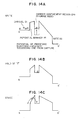
- data write operation can be effectuated by controlling the gate voltage.
- the gate voltage is at the low level V g0 .
- the threshold voltage at is set the high level V h .
- logic "1" of digital data can be written in the semiconductor element according to the invention.
- the gate voltage is swept in the negative direction to the zero volt level to thereby change the threshold voltage to the low level V l . In this way, logic "0" of digital data can be written.
- condition given by the expression (1) can apply valid when the capacitance C gt between the gate region and the carrier confinement region as well as the capacitance C between the carrier confinement region and the channel region is sufficiently small.
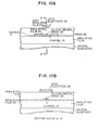
- the thickness of the semiconductor thin film (48) formed of silicon (Si) will have to be smaller than 9 nm inclusive in order that the barrier is effective at a room temperature.
- the small grain size mentioned above contributes to realization of small capacitance between the gate electrode and the channel region, the reason for which will be elucidated below.
- the current flow takes place due to migration or transfer of electrons from one to another crystals grain.
- the current path is extremely fine or thin because of a very small grain size as mentioned above. Consequently, the region in which electrons exists is remarkably small when compared with whole the channel region. For this reason, the capacitance C gc which is effective between the gate electrode and the effective channel portion (in the sense defined hereinbefore) is significantly small.
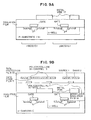
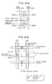
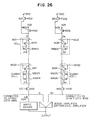
- FIG. 6 shows a structure of a memory IC device in which polycrystalline silicon memory elements each having the structure shown in Fig. 1 are employed.
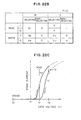
- each of the semiconductor elements or the polycrystalline silicon memory elements has such hysteresis characteristic as illustrated in Fig. 7. More specifically, it is presumed that when a voltage V w is applied between the gate and the source, the memory element takes on logic "1" state (state of high threshold value represented by V h ) while upon application of a voltage of -V w between the gate and the source, the memory element assumes logic "0" state (low threshold state V l ).
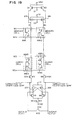
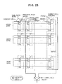
- reading of information or data is carried out in a manner described below (see Fig. 6).
- the data wire is connected to a voltage source via a load element.
- the other end of the data wire is connected to a sense amplifier.
- the potential of the word wire 1 as selected is set to the level of zero volt while the potential on the other word wire 2 not selected is set to the voltage level of -V w /2.
- the memory element MP1 is in the logic "1" state, this means that the memory element MP1 is in the off-state (i.e., nonconducting state) with the data wire remaining in the logically high state.
- the source and the drain may be formed of other semiconductor material or metal and that the insulation film may also be formed with other compositions so long as the capacitance C gc satisfying the requisite conditions mentioned previously can be realized.
- the dummy cell MM54 connected to the same word wire assumes the on-state.
- the preamplifier PA52 operates to cause the main data wire MD 52 to be discharged. Thus, the potential of the main data wire MD 52 is lowered.
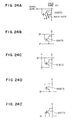
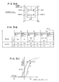
- Figs. 28A and 28B show a circuit configuration and a layout of a semiconductor memory device including a number of memory cells each of the structure shown in Fig. 27A which corresponds to four bits.
- the memory cells MM101 to 104 are each constituted by the polycrystalline silicon memory element described hereinbefore in conjunction with the first embodiment.
- the word wires for the adjacent memory cells are constituted by one and the same electrode, while a contact is shared in common by the two adjacent memory cells and connected to the data wire. It will thus be understood that the area required for implementation of the memory cell can significantly be decreased.
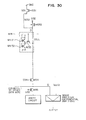
- the data wire D For writing logic "0" in the memory cell, the data wire D is set to the write voltage level V p . As a result of this, the memory element MM31 assumes the low threshold state with the memory element MM32 in the high threshold state. In succession to the write operation, the potential level of the data wire is set to V cc /2, which results in application of voltage of about V cc /2 between the gates and the sources of the memory elements MM31 and MM32, respectively. In the logic "1" state, the data wire D tends to discharge, while in the state of logic "0", the data wire D is charged. This trend or state is detected by the differential amplifier for reading the data or information, as can be seen in Fig. 30.
- the memory devices according to the invention can very profitably be employed as a main memory of a microprocessor in a data processing system such as shown in Fig. 34. Since the memory device according to the instant embodiment is nonvolatile, information stored once in the memory device can be held even after a source power supply is interrupted. Owing to this feature, the external storage implemented in the form of a hard disk or floppy disk can be realized by a memory chip fabricated according to the teachings of the invention. Besides, because of nonvolatileness of the main memory, a computer incorporating this type of main memory can instantaneously be restored to the state prevailing immediately before interruption of the power supply.
Landscapes
- Engineering & Computer Science (AREA)
- Microelectronics & Electronic Packaging (AREA)
- Chemical & Material Sciences (AREA)
- Computer Hardware Design (AREA)
- Nanotechnology (AREA)
- Physics & Mathematics (AREA)
- Theoretical Computer Science (AREA)
- Crystallography & Structural Chemistry (AREA)
- Mathematical Physics (AREA)
- Manufacturing & Machinery (AREA)
- Semiconductor Memories (AREA)
- Non-Volatile Memory (AREA)
- Insulated Gate Type Field-Effect Transistor (AREA)
- Read Only Memory (AREA)
Applications Claiming Priority (6)
| Application Number | Priority Date | Filing Date | Title |
|---|---|---|---|
| JP20492293 | 1993-08-19 | ||
| JP20492293 | 1993-08-19 | ||
| JP29163893A JP3613594B2 (ja) | 1993-08-19 | 1993-11-22 | 半導体素子およびこれを用いた半導体記憶装置 |
| JP29163893 | 1993-11-22 | ||
| EP94112656A EP0642173B1 (fr) | 1993-08-19 | 1994-08-12 | Elément semi-conducteur et dispositif de mémoire à semi-conducteur |
| EP98124768A EP0933820B1 (fr) | 1993-08-19 | 1994-08-12 | Elémemt semi-conducteur et dispositif de mémoire semi-conductrice l'utilisant |
Related Parent Applications (2)
| Application Number | Title | Priority Date | Filing Date |
|---|---|---|---|
| EP94112656.7 Division | 1994-08-12 | ||
| EP98124768.7 Division | 1998-12-28 |
Publications (1)
| Publication Number | Publication Date |
|---|---|
| EP1204146A1 true EP1204146A1 (fr) | 2002-05-08 |
Family
ID=26514741
Family Applications (5)
| Application Number | Title | Priority Date | Filing Date |
|---|---|---|---|
| EP01128059A Withdrawn EP1204147A1 (fr) | 1993-08-19 | 1994-08-12 | Elément semi-conducteur et dispositif de mémoire semi-conductrice l'utilisant |
| EP94112656A Expired - Lifetime EP0642173B1 (fr) | 1993-08-19 | 1994-08-12 | Elément semi-conducteur et dispositif de mémoire à semi-conducteur |
| EP01128058A Withdrawn EP1204146A1 (fr) | 1993-08-19 | 1994-08-12 | Elément semi-conducteur et dispositif de mémoire semi-conductrice l'utilisant |
| EP98101633A Expired - Lifetime EP0844671B1 (fr) | 1993-08-19 | 1994-08-12 | Elément à semi-conducteur et dispositif de mémoire à semi-conducteur utilisant cet élément |
| EP98124768A Expired - Lifetime EP0933820B1 (fr) | 1993-08-19 | 1994-08-12 | Elémemt semi-conducteur et dispositif de mémoire semi-conductrice l'utilisant |
Family Applications Before (2)
| Application Number | Title | Priority Date | Filing Date |
|---|---|---|---|
| EP01128059A Withdrawn EP1204147A1 (fr) | 1993-08-19 | 1994-08-12 | Elément semi-conducteur et dispositif de mémoire semi-conductrice l'utilisant |
| EP94112656A Expired - Lifetime EP0642173B1 (fr) | 1993-08-19 | 1994-08-12 | Elément semi-conducteur et dispositif de mémoire à semi-conducteur |
Family Applications After (2)
| Application Number | Title | Priority Date | Filing Date |
|---|---|---|---|
| EP98101633A Expired - Lifetime EP0844671B1 (fr) | 1993-08-19 | 1994-08-12 | Elément à semi-conducteur et dispositif de mémoire à semi-conducteur utilisant cet élément |
| EP98124768A Expired - Lifetime EP0933820B1 (fr) | 1993-08-19 | 1994-08-12 | Elémemt semi-conducteur et dispositif de mémoire semi-conductrice l'utilisant |
Country Status (6)
| Country | Link |
|---|---|
| US (9) | US5600163A (fr) |
| EP (5) | EP1204147A1 (fr) |
| JP (1) | JP3613594B2 (fr) |
| KR (1) | KR100342931B1 (fr) |
| CN (4) | CN1052344C (fr) |
| DE (3) | DE69432128T2 (fr) |
Cited By (76)
| Publication number | Priority date | Publication date | Assignee | Title |
|---|---|---|---|---|
| US6559470B2 (en) | 2000-06-22 | 2003-05-06 | Progressed Technologies, Inc. | Negative differential resistance field effect transistor (NDR-FET) and circuits using the same |
| US6567292B1 (en) | 2002-06-28 | 2003-05-20 | Progressant Technologies, Inc. | Negative differential resistance (NDR) element and memory with reduced soft error rate |
| US6594193B2 (en) | 2000-06-22 | 2003-07-15 | Progressent Technologies, Inc. | Charge pump for negative differential resistance transistor |
| US6724655B2 (en) | 2000-06-22 | 2004-04-20 | Progressant Technologies, Inc. | Memory cell using negative differential resistance field effect transistors |
| US6795337B2 (en) | 2002-06-28 | 2004-09-21 | Progressant Technologies, Inc. | Negative differential resistance (NDR) elements and memory device using the same |
| US6806117B2 (en) | 2002-12-09 | 2004-10-19 | Progressant Technologies, Inc. | Methods of testing/stressing a charge trapping device |
| US6812084B2 (en) | 2002-12-09 | 2004-11-02 | Progressant Technologies, Inc. | Adaptive negative differential resistance device |
| US6847562B2 (en) | 2002-06-28 | 2005-01-25 | Progressant Technologies, Inc. | Enhanced read and write methods for negative differential resistance (NDR) based memory device |
| US6849483B2 (en) | 2002-12-09 | 2005-02-01 | Progressant Technologies, Inc. | Charge trapping device and method of forming the same |
| US6853035B1 (en) | 2002-06-28 | 2005-02-08 | Synopsys, Inc. | Negative differential resistance (NDR) memory device with reduced soft error rate |
| US6864104B2 (en) | 2002-06-28 | 2005-03-08 | Progressant Technologies, Inc. | Silicon on insulator (SOI) negative differential resistance (NDR) based memory device with reduced body effects |
| US6873539B1 (en) | 2001-06-18 | 2005-03-29 | Pierre Fazan | Semiconductor device |
| US6894327B1 (en) | 2001-12-21 | 2005-05-17 | Progressant Technologies, Inc. | Negative differential resistance pull up element |
| US6912150B2 (en) | 2003-05-13 | 2005-06-28 | Lionel Portman | Reference current generator, and method of programming, adjusting and/or operating same |
| US6912151B2 (en) | 2002-06-28 | 2005-06-28 | Synopsys, Inc. | Negative differential resistance (NDR) based memory device with reduced body effects |
| US6979580B2 (en) | 2002-12-09 | 2005-12-27 | Progressant Technologies, Inc. | Process for controlling performance characteristics of a negative differential resistance (NDR) device |
| US6980467B2 (en) | 2002-12-09 | 2005-12-27 | Progressant Technologies, Inc. | Method of forming a negative differential resistance device |
| US6982918B2 (en) | 2002-04-18 | 2006-01-03 | Pierre Fazan | Data storage device and refreshing method for use with such device |
| US7005711B2 (en) | 2002-12-20 | 2006-02-28 | Progressant Technologies, Inc. | N-channel pull-up element and logic circuit |
| US7012833B2 (en) | 2002-12-09 | 2006-03-14 | Progressant Technologies, Inc. | Integrated circuit having negative differential resistance (NDR) devices with varied peak-to-valley ratios (PVRs) |
| US7061050B2 (en) | 2002-04-18 | 2006-06-13 | Innovative Silicon S.A. | Semiconductor device utilizing both fully and partially depleted devices |
| US7085153B2 (en) | 2003-05-13 | 2006-08-01 | Innovative Silicon S.A. | Semiconductor memory cell, array, architecture and device, and method of operating same |
| US7095659B2 (en) | 2002-06-28 | 2006-08-22 | Progressant Technologies, Inc. | Variable voltage supply bias and methods for negative differential resistance (NDR) based memory device |
| US7098472B2 (en) | 2002-06-28 | 2006-08-29 | Progressant Technologies, Inc. | Negative differential resistance (NDR) elements and memory device using the same |
| US7184298B2 (en) | 2003-09-24 | 2007-02-27 | Innovative Silicon S.A. | Low power programming technique for a floating body memory transistor, memory cell, and memory array |
| US7187581B2 (en) | 2003-05-13 | 2007-03-06 | Innovative Silicon S.A. | Semiconductor memory device and method of operating same |
| US7251164B2 (en) | 2004-11-10 | 2007-07-31 | Innovative Silicon S.A. | Circuitry for and method of improving statistical distribution of integrated circuits |
| US7301838B2 (en) | 2004-12-13 | 2007-11-27 | Innovative Silicon S.A. | Sense amplifier circuitry and architecture to write data into and/or read from memory cells |
| US7301803B2 (en) | 2004-12-22 | 2007-11-27 | Innovative Silicon S.A. | Bipolar reading technique for a memory cell having an electrically floating body transistor |
| US7355916B2 (en) | 2005-09-19 | 2008-04-08 | Innovative Silicon S.A. | Method and circuitry to generate a reference current for reading a memory cell, and device implementing same |
| US7453083B2 (en) | 2001-12-21 | 2008-11-18 | Synopsys, Inc. | Negative differential resistance field effect transistor for implementing a pull up element in a memory cell |
| US7476939B2 (en) | 2004-11-04 | 2009-01-13 | Innovative Silicon Isi Sa | Memory cell having an electrically floating body transistor and programming technique therefor |
| US7492632B2 (en) | 2006-04-07 | 2009-02-17 | Innovative Silicon Isi Sa | Memory array having a programmable word length, and method of operating same |
| US7542345B2 (en) | 2006-02-16 | 2009-06-02 | Innovative Silicon Isi Sa | Multi-bit memory cell having electrically floating body transistor, and method of programming and reading same |
| US7542340B2 (en) | 2006-07-11 | 2009-06-02 | Innovative Silicon Isi Sa | Integrated circuit including memory array having a segmented bit line architecture and method of controlling and/or operating same |
| US7606098B2 (en) | 2006-04-18 | 2009-10-20 | Innovative Silicon Isi Sa | Semiconductor memory array architecture with grouped memory cells, and method of controlling same |
| US7606066B2 (en) | 2005-09-07 | 2009-10-20 | Innovative Silicon Isi Sa | Memory cell and memory cell array having an electrically floating body transistor, and methods of operating same |
| US7683430B2 (en) | 2005-12-19 | 2010-03-23 | Innovative Silicon Isi Sa | Electrically floating body memory cell and array, and method of operating or controlling same |
| US7736959B2 (en) | 2003-07-22 | 2010-06-15 | Innovative Silicon Isi Sa | Integrated circuit device, and method of fabricating same |
| US7924630B2 (en) | 2008-10-15 | 2011-04-12 | Micron Technology, Inc. | Techniques for simultaneously driving a plurality of source lines |
| US7933142B2 (en) | 2006-05-02 | 2011-04-26 | Micron Technology, Inc. | Semiconductor memory cell and array using punch-through to program and read same |
| US7933140B2 (en) | 2008-10-02 | 2011-04-26 | Micron Technology, Inc. | Techniques for reducing a voltage swing |
| US7947543B2 (en) | 2008-09-25 | 2011-05-24 | Micron Technology, Inc. | Recessed gate silicon-on-insulator floating body device with self-aligned lateral isolation |
| US7957206B2 (en) | 2008-04-04 | 2011-06-07 | Micron Technology, Inc. | Read circuitry for an integrated circuit having memory cells and/or a memory cell array, and method of operating same |
| US8014195B2 (en) | 2008-02-06 | 2011-09-06 | Micron Technology, Inc. | Single transistor memory cell |
| US8064274B2 (en) | 2007-05-30 | 2011-11-22 | Micron Technology, Inc. | Integrated circuit having voltage generation circuitry for memory cell array, and method of operating and/or controlling same |
| US8069377B2 (en) | 2006-06-26 | 2011-11-29 | Micron Technology, Inc. | Integrated circuit having memory array including ECC and column redundancy and method of operating the same |
| US8085594B2 (en) | 2007-06-01 | 2011-12-27 | Micron Technology, Inc. | Reading technique for memory cell with electrically floating body transistor |
| US8139418B2 (en) | 2009-04-27 | 2012-03-20 | Micron Technology, Inc. | Techniques for controlling a direct injection semiconductor memory device |
| US8174881B2 (en) | 2009-11-24 | 2012-05-08 | Micron Technology, Inc. | Techniques for reducing disturbance in a semiconductor device |
| US8189376B2 (en) | 2008-02-08 | 2012-05-29 | Micron Technology, Inc. | Integrated circuit having memory cells including gate material having high work function, and method of manufacturing same |
| US8194487B2 (en) | 2007-09-17 | 2012-06-05 | Micron Technology, Inc. | Refreshing data of memory cells with electrically floating body transistors |
| US8199595B2 (en) | 2009-09-04 | 2012-06-12 | Micron Technology, Inc. | Techniques for sensing a semiconductor memory device |
| US8213226B2 (en) | 2008-12-05 | 2012-07-03 | Micron Technology, Inc. | Vertical transistor memory cell and array |
| US8223574B2 (en) | 2008-11-05 | 2012-07-17 | Micron Technology, Inc. | Techniques for block refreshing a semiconductor memory device |
| US8264041B2 (en) | 2007-01-26 | 2012-09-11 | Micron Technology, Inc. | Semiconductor device with electrically floating body |
| US8310893B2 (en) | 2009-12-16 | 2012-11-13 | Micron Technology, Inc. | Techniques for reducing impact of array disturbs in a semiconductor memory device |
| US8315099B2 (en) | 2009-07-27 | 2012-11-20 | Micron Technology, Inc. | Techniques for providing a direct injection semiconductor memory device |
| US8319294B2 (en) | 2009-02-18 | 2012-11-27 | Micron Technology, Inc. | Techniques for providing a source line plane |
| US8349662B2 (en) | 2007-12-11 | 2013-01-08 | Micron Technology, Inc. | Integrated circuit having memory cell array, and method of manufacturing same |
| US8369177B2 (en) | 2010-03-05 | 2013-02-05 | Micron Technology, Inc. | Techniques for reading from and/or writing to a semiconductor memory device |
| US8411524B2 (en) | 2010-05-06 | 2013-04-02 | Micron Technology, Inc. | Techniques for refreshing a semiconductor memory device |
| US8411513B2 (en) | 2010-03-04 | 2013-04-02 | Micron Technology, Inc. | Techniques for providing a semiconductor memory device having hierarchical bit lines |
| US8416636B2 (en) | 2010-02-12 | 2013-04-09 | Micron Technology, Inc. | Techniques for controlling a semiconductor memory device |
| US8498157B2 (en) | 2009-05-22 | 2013-07-30 | Micron Technology, Inc. | Techniques for providing a direct injection semiconductor memory device |
| US8508994B2 (en) | 2009-04-30 | 2013-08-13 | Micron Technology, Inc. | Semiconductor device with floating gate and electrically floating body |
| US8518774B2 (en) | 2007-03-29 | 2013-08-27 | Micron Technology, Inc. | Manufacturing process for zero-capacitor random access memory circuits |
| US8531878B2 (en) | 2011-05-17 | 2013-09-10 | Micron Technology, Inc. | Techniques for providing a semiconductor memory device |
| US8537610B2 (en) | 2009-07-10 | 2013-09-17 | Micron Technology, Inc. | Techniques for providing a semiconductor memory device |
| US8536628B2 (en) | 2007-11-29 | 2013-09-17 | Micron Technology, Inc. | Integrated circuit having memory cell array including barriers, and method of manufacturing same |
| US8547738B2 (en) | 2010-03-15 | 2013-10-01 | Micron Technology, Inc. | Techniques for providing a semiconductor memory device |
| US8576631B2 (en) | 2010-03-04 | 2013-11-05 | Micron Technology, Inc. | Techniques for sensing a semiconductor memory device |
| US8710566B2 (en) | 2009-03-04 | 2014-04-29 | Micron Technology, Inc. | Techniques for forming a contact to a buried diffusion layer in a semiconductor memory device |
| US8748959B2 (en) | 2009-03-31 | 2014-06-10 | Micron Technology, Inc. | Semiconductor memory device |
| US8773933B2 (en) | 2012-03-16 | 2014-07-08 | Micron Technology, Inc. | Techniques for accessing memory cells |
| US9559216B2 (en) | 2011-06-06 | 2017-01-31 | Micron Technology, Inc. | Semiconductor memory device and method for biasing same |
Families Citing this family (65)
| Publication number | Priority date | Publication date | Assignee | Title |
|---|---|---|---|---|
| JP3613594B2 (ja) * | 1993-08-19 | 2005-01-26 | 株式会社ルネサステクノロジ | 半導体素子およびこれを用いた半導体記憶装置 |
| JPH08125034A (ja) * | 1993-12-03 | 1996-05-17 | Mitsubishi Electric Corp | 半導体記憶装置 |
| US5714766A (en) * | 1995-09-29 | 1998-02-03 | International Business Machines Corporation | Nano-structure memory device |
| JPH09312378A (ja) * | 1996-03-19 | 1997-12-02 | Fujitsu Ltd | 半導体装置及びその製造方法 |
| JP3320641B2 (ja) * | 1996-09-13 | 2002-09-03 | 株式会社東芝 | メモリセル |
| US6169308B1 (en) | 1996-11-15 | 2001-01-02 | Hitachi, Ltd. | Semiconductor memory device and manufacturing method thereof |
| EP0843361A1 (fr) * | 1996-11-15 | 1998-05-20 | Hitachi Europe Limited | Dispositif de mémoire |
| EP0843360A1 (fr) * | 1996-11-15 | 1998-05-20 | Hitachi Europe Limited | Dispositif de mémoire |
| US6753568B1 (en) | 1996-11-15 | 2004-06-22 | Hitachi, Ltd. | Memory device |
| US6642574B2 (en) | 1997-10-07 | 2003-11-04 | Hitachi, Ltd. | Semiconductor memory device and manufacturing method thereof |
| US5945686A (en) * | 1997-04-28 | 1999-08-31 | Hitachi, Ltd. | Tunneling electronic device |
| AT405109B (de) | 1997-05-21 | 1999-05-25 | Wasshuber Christoph Dipl Ing D | Ein-elektron speicherbauelement |
| US6060743A (en) * | 1997-05-21 | 2000-05-09 | Kabushiki Kaisha Toshiba | Semiconductor memory device having multilayer group IV nanocrystal quantum dot floating gate and method of manufacturing the same |
| JP3544101B2 (ja) * | 1997-06-04 | 2004-07-21 | ソニー株式会社 | 量子素子 |
| EP0926260A3 (fr) | 1997-12-12 | 2001-04-11 | Matsushita Electric Industrial Co., Ltd. | Formation d'une couche métallique d'un patron déterminé utilisant l'interaction entre anticorps et antigènes |
| JPH11214640A (ja) * | 1998-01-28 | 1999-08-06 | Hitachi Ltd | 半導体記憶素子、半導体記憶装置とその制御方法 |
| US6040605A (en) * | 1998-01-28 | 2000-03-21 | Hitachi, Ltd. | Semiconductor memory device |
| JP3214556B2 (ja) * | 1998-08-25 | 2001-10-02 | 日本電気株式会社 | 集積回路装置、半導体ウェハ、回路検査方法 |
| TW442837B (en) | 1998-12-03 | 2001-06-23 | Infineon Technologies Ag | Integrated circuit-arrangement and its production method |
| DE19858759C1 (de) * | 1998-12-18 | 2000-03-23 | Siemens Ag | Schaltungsanordnung mit mindestens einem nanoelektronischen Bauelement und Verfahren zu deren Herstellung |
| JP3955409B2 (ja) * | 1999-03-17 | 2007-08-08 | 株式会社ルネサステクノロジ | 半導体記憶装置 |
| US6501138B1 (en) * | 1999-04-16 | 2002-12-31 | Seiko Epson Corporation | Semiconductor memory device and method for manufacturing the same |
| US6548825B1 (en) | 1999-06-04 | 2003-04-15 | Matsushita Electric Industrial Co., Ltd. | Semiconductor device including barrier layer having dispersed particles |
| KR100343210B1 (ko) | 1999-08-11 | 2002-07-10 | 윤종용 | 단일 전자 충전 mnos계 메모리 및 그 구동 방법 |
| TWI243432B (en) * | 1999-10-29 | 2005-11-11 | Hitachi Ltd | Semiconductor device, method of making the same and liquid crystal display device |
| KR100340929B1 (ko) * | 1999-11-25 | 2002-06-20 | 오길록 | 금속 초박막을 이용한 단전자 트랜지스터 |
| KR100360496B1 (ko) | 2000-04-15 | 2002-11-13 | 삼성전자 주식회사 | 이중 양자점 응용 단일 전자 다치 메모리 및 그 구동방법 |
| DE10023871C1 (de) * | 2000-05-16 | 2001-09-27 | Infineon Technologies Ag | Feldeffekttransistor und Verfahren zum Herstellen eines Feldeffekttransistors |
| JP4083975B2 (ja) * | 2000-12-11 | 2008-04-30 | 株式会社ルネサステクノロジ | 半導体装置 |
| FR2818439B1 (fr) * | 2000-12-18 | 2003-09-26 | Commissariat Energie Atomique | Procede de fabrication d'un ilot de matiere confine entre des electrodes, et applications aux transistors |
| JP2003187586A (ja) * | 2001-12-14 | 2003-07-04 | Hitachi Ltd | 不揮発性半導体記憶装置および情報処理装置 |
| US20040130942A1 (en) * | 2003-01-02 | 2004-07-08 | Macronix International Co., Ltd. | Data retention for a localized trapping non-volatile memory |
| US6764883B1 (en) * | 2003-01-07 | 2004-07-20 | International Business Machines Corp. | Amorphous and polycrystalline silicon nanolaminate |
| JP4307919B2 (ja) * | 2003-06-27 | 2009-08-05 | 三洋電機株式会社 | 半導体装置の製造方法 |
| US7122413B2 (en) | 2003-12-19 | 2006-10-17 | Texas Instruments Incorporated | Method to manufacture silicon quantum islands and single-electron devices |
| JP4445299B2 (ja) * | 2004-03-18 | 2010-04-07 | 富士通株式会社 | 不揮発性メモリ評価方法 |
| WO2006030489A1 (fr) * | 2004-09-14 | 2006-03-23 | Idemitsu Kosan Co., Ltd. | Formulation d’huile pour réfrigérateur |
| CN101361189B (zh) * | 2005-01-25 | 2011-02-16 | 莫克斯托尼克斯股份有限公司 | 高性能fet器件和方法 |
| KR100594327B1 (ko) * | 2005-03-24 | 2006-06-30 | 삼성전자주식회사 | 라운드 형태의 단면을 가지는 나노와이어를 구비한 반도체소자 및 그 제조 방법 |
| US7368789B1 (en) * | 2005-06-13 | 2008-05-06 | Actel Corporation | Non-volatile programmable memory cell and array for programmable logic array |
| US20070007576A1 (en) * | 2005-07-07 | 2007-01-11 | Samsung Electronics Co., Ltd. | Multi-bit storageable non-volatile memory device |
| US7492048B2 (en) | 2006-01-10 | 2009-02-17 | International Business Machines Corporation | CMOS sensors having charge pushing regions |
| US7494850B2 (en) | 2006-02-15 | 2009-02-24 | International Business Machines Corporation | Ultra-thin logic and backgated ultra-thin SRAM |
| US7619257B2 (en) * | 2006-02-16 | 2009-11-17 | Alcatel-Lucent Usa Inc. | Devices including graphene layers epitaxially grown on single crystal substrates |
| US20080083943A1 (en) * | 2006-10-10 | 2008-04-10 | Walker Andrew J | Dual-gate memory device and optimization of electrical interaction between front and back gates to enable scaling |
| US7777268B2 (en) * | 2006-10-10 | 2010-08-17 | Schiltron Corp. | Dual-gate device |
| US7812370B2 (en) | 2007-07-25 | 2010-10-12 | Taiwan Semiconductor Manufacturing Company, Ltd. | Tunnel field-effect transistor with narrow band-gap channel and strong gate coupling |
| JP5183187B2 (ja) | 2007-12-14 | 2013-04-17 | キヤノン株式会社 | 液体吐出ヘッド |
| US8004871B2 (en) * | 2008-05-26 | 2011-08-23 | Panasonic Corporation | Semiconductor memory device including FET memory elements |
| US7834345B2 (en) * | 2008-09-05 | 2010-11-16 | Taiwan Semiconductor Manufacturing Company, Ltd. | Tunnel field-effect transistors with superlattice channels |
| US8587075B2 (en) * | 2008-11-18 | 2013-11-19 | Taiwan Semiconductor Manufacturing Company, Ltd. | Tunnel field-effect transistor with metal source |
| TWI382530B (zh) * | 2009-04-03 | 2013-01-11 | Acer Inc | A method and device for utilizing thin film transistor as nonvolatile memory |
| US8155905B2 (en) * | 2009-07-21 | 2012-04-10 | Hitachi, Ltd. | Method of extracting a time constant from complex random telegraph signals |
| KR101796116B1 (ko) | 2010-10-20 | 2017-11-10 | 삼성전자 주식회사 | 반도체 장치, 이를 포함하는 메모리 모듈, 메모리 시스템 및 그 동작방법 |
| US9793220B2 (en) * | 2012-03-16 | 2017-10-17 | Intel Deutschland Gmbh | Detection of environmental conditions in a semiconductor chip |
| US8860123B1 (en) | 2013-03-28 | 2014-10-14 | Stmicroelectronics, Inc. | Memory device having multiple dielectric gate stacks with first and second dielectric layers and related methods |
| US9006816B2 (en) | 2013-03-28 | 2015-04-14 | Stmicroelectronics, Inc. | Memory device having multiple dielectric gate stacks and related methods |
| TWI521377B (zh) * | 2014-07-21 | 2016-02-11 | 群聯電子股份有限公司 | 積體電路、密碼生成的方法以及資料交換的方法 |
| FR3057105A1 (fr) * | 2016-10-05 | 2018-04-06 | Commissariat A L'energie Atomique Et Aux Energies Alternatives | Dispositif a boite(s) quantique(s) comportant des dopants localises dans une couche semi-conductrice mince |
| US10396076B2 (en) | 2017-03-21 | 2019-08-27 | International Business Machines Corporation | Structure and method for multiple threshold voltage definition in advanced CMOS device technology |
| JP7108386B2 (ja) * | 2017-08-24 | 2022-07-28 | 住友化学株式会社 | 電荷トラップ評価方法 |
| KR102528205B1 (ko) * | 2018-06-26 | 2023-05-03 | 에스케이하이닉스 주식회사 | 매립 채널 어레이 트랜지스터를 포함하는 극저온 반도체 소자 |
| JP7818259B2 (ja) * | 2021-06-24 | 2026-02-20 | 学校法人帝京大学 | 量子装置 |
| CN113764137B (zh) * | 2021-08-25 | 2024-01-09 | 湖南兴威新材料有限公司 | 纳米银线导电膜的制备方法、纳米银线导电膜及其应用 |
| KR20240020052A (ko) * | 2022-08-05 | 2024-02-14 | 에스케이하이닉스 주식회사 | 반도체 장치 및 그 제조 방법 |
Citations (6)
| Publication number | Priority date | Publication date | Assignee | Title |
|---|---|---|---|---|
| DE2149303A1 (de) * | 1970-10-02 | 1972-04-06 | Ibm | Halbleiter-Speichervorrichtung |
| DE2152225A1 (de) * | 1970-10-27 | 1972-05-10 | Shumpei Yamazaki | Halbleiteranordnung |
| EP0107039A2 (fr) * | 1982-09-30 | 1984-05-02 | International Business Machines Corporation | Dispositif semi-conducteur de transmission à résonance et circuit comportant ce dispositif |
| JPH03141676A (ja) * | 1989-10-26 | 1991-06-17 | Rohm Co Ltd | 半導体記憶装置 |
| JPH05129632A (ja) * | 1991-10-31 | 1993-05-25 | Rohm Co Ltd | 電荷トラツプ膜 |
| US5357134A (en) * | 1991-10-31 | 1994-10-18 | Rohm Co., Ltd. | Nonvolatile semiconductor device having charge trap film containing silicon crystal grains |
Family Cites Families (36)
| Publication number | Priority date | Publication date | Assignee | Title |
|---|---|---|---|---|
| US537134A (en) * | 1895-04-09 | Haeey toechiani | ||
| US3878549A (en) * | 1970-10-27 | 1975-04-15 | Shumpei Yamazaki | Semiconductor memories |
| JPS5213782A (en) * | 1975-07-23 | 1977-02-02 | Hitachi Ltd | Semiconductor non-vol atile memory unit |
| US4047974A (en) * | 1975-12-30 | 1977-09-13 | Hughes Aircraft Company | Process for fabricating non-volatile field effect semiconductor memory structure utilizing implanted ions to induce trapping states |
| US4173791A (en) * | 1977-09-16 | 1979-11-06 | Fairchild Camera And Instrument Corporation | Insulated gate field-effect transistor read-only memory array |
| DE3280144D1 (de) | 1981-05-15 | 1990-05-03 | Matsushita Electric Industrial Co Ltd | Verfahren zur herstellung eines magnetischen aufzeichnungstraegers. |
| US4503447A (en) * | 1982-07-16 | 1985-03-05 | The United States Of America As Represented By The Secretary Of The Army | Multi-dimensional quantum well device |
| JPS5974680A (ja) * | 1982-10-20 | 1984-04-27 | Mitsubishi Electric Corp | 半導体不揮発性メモリ装置およびその製造方法 |
| US4748485A (en) * | 1985-03-21 | 1988-05-31 | Hughes Aircraft Company | Opposed dual-gate hybrid structure for three-dimensional integrated circuits |
| JPH0777264B2 (ja) * | 1986-04-02 | 1995-08-16 | 三菱電機株式会社 | 薄膜トランジスタの製造方法 |
| US5140391A (en) * | 1987-08-24 | 1992-08-18 | Sony Corporation | Thin film MOS transistor having pair of gate electrodes opposing across semiconductor layer |
| JPH02109341A (ja) * | 1988-10-19 | 1990-04-23 | Fuji Xerox Co Ltd | 薄膜トランジスタの製造方法 |
| CA2001682C (fr) * | 1988-10-28 | 1994-05-03 | Hiroshi Matsumoto | Transistor en couches minces a fonction de memorisation et methode pour utiliser ce transistor comme element de memoire |
| US5079606A (en) * | 1989-01-26 | 1992-01-07 | Casio Computer Co., Ltd. | Thin-film memory element |
| US5120672A (en) * | 1989-02-22 | 1992-06-09 | Texas Instruments Incorporated | Fabricating a single level merged EEPROM cell having an ONO memory stack substantially spaced from the source region |
| US5019882A (en) * | 1989-05-15 | 1991-05-28 | International Business Machines Corporation | Germanium channel silicon MOSFET |
| US4987463A (en) * | 1989-08-28 | 1991-01-22 | Motorola, Inc. | FET having a high trap concentration interface layer |
| JPH03253072A (ja) * | 1990-03-02 | 1991-11-12 | Hitachi Ltd | 半導体装置 |
| US5198379A (en) * | 1990-04-27 | 1993-03-30 | Sharp Kabushiki Kaisha | Method of making a MOS thin film transistor with self-aligned asymmetrical structure |
| US5075237A (en) * | 1990-07-26 | 1991-12-24 | Industrial Technology Research Institute | Process of making a high photosensitive depletion-gate thin film transistor |
| KR920008834A (ko) * | 1990-10-09 | 1992-05-28 | 아이자와 스스무 | 박막 반도체 장치 |
| US5420048A (en) * | 1991-01-09 | 1995-05-30 | Canon Kabushiki Kaisha | Manufacturing method for SOI-type thin film transistor |
| JP3556679B2 (ja) * | 1992-05-29 | 2004-08-18 | 株式会社半導体エネルギー研究所 | 電気光学装置 |
| JPH05129630A (ja) * | 1991-10-31 | 1993-05-25 | Rohm Co Ltd | 不揮発性半導体記憶装置の製造方法 |
| US5420055A (en) * | 1992-01-22 | 1995-05-30 | Kopin Corporation | Reduction of parasitic effects in floating body MOSFETs |
| FR2688090B1 (fr) * | 1992-02-27 | 1994-04-08 | Commissariat A Energie Atomique | Cellule memoire non volatile du type metal-ferroelectrique semi-conducteur. |
| JP3254007B2 (ja) * | 1992-06-09 | 2002-02-04 | 株式会社半導体エネルギー研究所 | 薄膜状半導体装置およびその作製方法 |
| US5461250A (en) * | 1992-08-10 | 1995-10-24 | International Business Machines Corporation | SiGe thin film or SOI MOSFET and method for making the same |
| JPH0669515A (ja) * | 1992-08-19 | 1994-03-11 | Fujitsu Ltd | 半導体記憶装置 |
| JP2541087B2 (ja) * | 1992-10-30 | 1996-10-09 | 日本電気株式会社 | 不揮発性半導体記憶装置のデ―タ消去方法 |
| US5359219A (en) * | 1992-12-04 | 1994-10-25 | Texas Instruments Incorporated | Silicon on insulator device comprising improved substrate doping |
| JPH0799251A (ja) * | 1992-12-10 | 1995-04-11 | Sony Corp | 半導体メモリセル |
| JP3613594B2 (ja) * | 1993-08-19 | 2005-01-26 | 株式会社ルネサステクノロジ | 半導体素子およびこれを用いた半導体記憶装置 |
| JP3141676B2 (ja) | 1994-02-03 | 2001-03-05 | トヨタ自動車株式会社 | 車両運動検出装置およびその検出感度調整方法 |
| DE10147858A1 (de) * | 2001-09-27 | 2003-04-30 | Itw Gema Ag | Spritzbeschichtungsvorrichtung |
| US6580132B1 (en) * | 2002-04-10 | 2003-06-17 | International Business Machines Corporation | Damascene double-gate FET |
-
1993
- 1993-11-22 JP JP29163893A patent/JP3613594B2/ja not_active Expired - Fee Related
-
1994
- 1994-08-12 EP EP01128059A patent/EP1204147A1/fr not_active Withdrawn
- 1994-08-12 DE DE69432128T patent/DE69432128T2/de not_active Expired - Fee Related
- 1994-08-12 DE DE69431810T patent/DE69431810T2/de not_active Expired - Fee Related
- 1994-08-12 EP EP94112656A patent/EP0642173B1/fr not_active Expired - Lifetime
- 1994-08-12 EP EP01128058A patent/EP1204146A1/fr not_active Withdrawn
- 1994-08-12 EP EP98101633A patent/EP0844671B1/fr not_active Expired - Lifetime
- 1994-08-12 DE DE69419469T patent/DE69419469T2/de not_active Expired - Fee Related
- 1994-08-12 EP EP98124768A patent/EP0933820B1/fr not_active Expired - Lifetime
- 1994-08-16 US US08/291,752 patent/US5600163A/en not_active Expired - Lifetime
- 1994-08-17 KR KR1019940020261A patent/KR100342931B1/ko not_active Expired - Fee Related
- 1994-08-19 CN CN94109104A patent/CN1052344C/zh not_active Expired - Fee Related
-
1997
- 1997-04-01 CN CN97110215A patent/CN1086842C/zh not_active Expired - Fee Related
- 1997-04-01 CN CN97110214A patent/CN1112732C/zh not_active Expired - Fee Related
-
1998
- 1998-07-30 US US09/126,437 patent/US6104056A/en not_active Expired - Lifetime
-
2000
- 2000-03-09 US US09/521,970 patent/US6291852B1/en not_active Expired - Fee Related
-
2001
- 2001-07-27 US US09/915,588 patent/US6674117B2/en not_active Expired - Fee Related
- 2001-08-31 US US09/943,444 patent/US6555882B2/en not_active Expired - Fee Related
-
2002
- 2002-06-05 CN CNB021220832A patent/CN1204627C/zh not_active Expired - Fee Related
-
2003
- 2003-08-29 US US10/650,732 patent/US6787841B2/en not_active Expired - Fee Related
-
2004
- 2004-08-31 US US10/929,424 patent/US7061053B2/en not_active Expired - Fee Related
-
2006
- 2006-05-24 US US11/439,152 patent/US7309892B2/en not_active Expired - Fee Related
-
2007
- 2007-10-31 US US11/931,369 patent/US20080061298A1/en not_active Abandoned
Patent Citations (6)
| Publication number | Priority date | Publication date | Assignee | Title |
|---|---|---|---|---|
| DE2149303A1 (de) * | 1970-10-02 | 1972-04-06 | Ibm | Halbleiter-Speichervorrichtung |
| DE2152225A1 (de) * | 1970-10-27 | 1972-05-10 | Shumpei Yamazaki | Halbleiteranordnung |
| EP0107039A2 (fr) * | 1982-09-30 | 1984-05-02 | International Business Machines Corporation | Dispositif semi-conducteur de transmission à résonance et circuit comportant ce dispositif |
| JPH03141676A (ja) * | 1989-10-26 | 1991-06-17 | Rohm Co Ltd | 半導体記憶装置 |
| JPH05129632A (ja) * | 1991-10-31 | 1993-05-25 | Rohm Co Ltd | 電荷トラツプ膜 |
| US5357134A (en) * | 1991-10-31 | 1994-10-18 | Rohm Co., Ltd. | Nonvolatile semiconductor device having charge trap film containing silicon crystal grains |
Non-Patent Citations (2)
| Title |
|---|
| PATENT ABSTRACTS OF JAPAN vol. 015, no. 359 (E - 1110) 11 September 1991 (1991-09-11) * |
| PATENT ABSTRACTS OF JAPAN vol. 017, no. 504 (E - 1430) 10 September 1993 (1993-09-10) * |
Cited By (161)
| Publication number | Priority date | Publication date | Assignee | Title |
|---|---|---|---|---|
| US6724655B2 (en) | 2000-06-22 | 2004-04-20 | Progressant Technologies, Inc. | Memory cell using negative differential resistance field effect transistors |
| US6559470B2 (en) | 2000-06-22 | 2003-05-06 | Progressed Technologies, Inc. | Negative differential resistance field effect transistor (NDR-FET) and circuits using the same |
| US6594193B2 (en) | 2000-06-22 | 2003-07-15 | Progressent Technologies, Inc. | Charge pump for negative differential resistance transistor |
| US6937516B2 (en) | 2001-06-18 | 2005-08-30 | Innovative Silicon S.A. | Semiconductor device |
| US7732816B2 (en) | 2001-06-18 | 2010-06-08 | Innovative Silicon Isi Sa | Semiconductor device |
| US7280399B2 (en) | 2001-06-18 | 2007-10-09 | Innovative Silicon S.A. | Semiconductor device |
| US6925006B2 (en) | 2001-06-18 | 2005-08-02 | Innovative Silicon S.A. | Semiconductor device |
| US7239549B2 (en) | 2001-06-18 | 2007-07-03 | Innovative Silicon S.A. | Semiconductor device |
| US7541616B2 (en) | 2001-06-18 | 2009-06-02 | Innovative Silicon Isi Sa | Semiconductor device |
| US6969662B2 (en) | 2001-06-18 | 2005-11-29 | Pierre Fazan | Semiconductor device |
| US6873539B1 (en) | 2001-06-18 | 2005-03-29 | Pierre Fazan | Semiconductor device |
| US6934186B2 (en) | 2001-06-18 | 2005-08-23 | Innovative Silicon S.A. | Semiconductor device |
| US6930918B2 (en) | 2001-06-18 | 2005-08-16 | Innovative Silicon S.A. | Semiconductor device |
| US6956262B1 (en) | 2001-12-21 | 2005-10-18 | Synopsys Inc. | Charge trapping pull up element |
| US6724024B1 (en) | 2001-12-21 | 2004-04-20 | Progressant Technologies, Inc. | Field effect transistor pull-up/load element |
| US6894327B1 (en) | 2001-12-21 | 2005-05-17 | Progressant Technologies, Inc. | Negative differential resistance pull up element |
| US7995380B2 (en) | 2001-12-21 | 2011-08-09 | Synopsys, Inc. | Negative differential resistance pull up element for DRAM |
| US6933548B1 (en) | 2001-12-21 | 2005-08-23 | Synopsys, Inc. | Negative differential resistance load element |
| US7453083B2 (en) | 2001-12-21 | 2008-11-18 | Synopsys, Inc. | Negative differential resistance field effect transistor for implementing a pull up element in a memory cell |
| US7342842B2 (en) | 2002-04-18 | 2008-03-11 | Innovative Silicon, S.A. | Data storage device and refreshing method for use with such device |
| US7514748B2 (en) | 2002-04-18 | 2009-04-07 | Innovative Silicon Isi Sa | Semiconductor device |
| US7061050B2 (en) | 2002-04-18 | 2006-06-13 | Innovative Silicon S.A. | Semiconductor device utilizing both fully and partially depleted devices |
| US7170807B2 (en) | 2002-04-18 | 2007-01-30 | Innovative Silicon S.A. | Data storage device and refreshing method for use with such device |
| US6982918B2 (en) | 2002-04-18 | 2006-01-03 | Pierre Fazan | Data storage device and refreshing method for use with such device |
| US6847562B2 (en) | 2002-06-28 | 2005-01-25 | Progressant Technologies, Inc. | Enhanced read and write methods for negative differential resistance (NDR) based memory device |
| US7012842B2 (en) | 2002-06-28 | 2006-03-14 | Progressant Technologies, Inc. | Enhanced read and write methods for negative differential resistance (NDR) based memory device |
| US6795337B2 (en) | 2002-06-28 | 2004-09-21 | Progressant Technologies, Inc. | Negative differential resistance (NDR) elements and memory device using the same |
| US7095659B2 (en) | 2002-06-28 | 2006-08-22 | Progressant Technologies, Inc. | Variable voltage supply bias and methods for negative differential resistance (NDR) based memory device |
| US6853035B1 (en) | 2002-06-28 | 2005-02-08 | Synopsys, Inc. | Negative differential resistance (NDR) memory device with reduced soft error rate |
| US6990016B2 (en) | 2002-06-28 | 2006-01-24 | Progressant Technologies, Inc. | Method of making memory cell utilizing negative differential resistance devices |
| US6727548B1 (en) | 2002-06-28 | 2004-04-27 | Progressant Technologies, Inc. | Negative differential resistance (NDR) element and memory with reduced soft error rate |
| US6912151B2 (en) | 2002-06-28 | 2005-06-28 | Synopsys, Inc. | Negative differential resistance (NDR) based memory device with reduced body effects |
| US6567292B1 (en) | 2002-06-28 | 2003-05-20 | Progressant Technologies, Inc. | Negative differential resistance (NDR) element and memory with reduced soft error rate |
| US7187028B2 (en) | 2002-06-28 | 2007-03-06 | Synopsys, Inc. | Silicon on insulator (SOI) negative differential resistance (NDR) based memory device with reduced body effects |
| US7016224B2 (en) | 2002-06-28 | 2006-03-21 | Tsu-Jae King | Two terminal silicon based negative differential resistance device |
| US6861707B1 (en) | 2002-06-28 | 2005-03-01 | Progressant Technologies, Inc. | Negative differential resistance (NDR) memory cell with reduced soft error rate |
| US6864104B2 (en) | 2002-06-28 | 2005-03-08 | Progressant Technologies, Inc. | Silicon on insulator (SOI) negative differential resistance (NDR) based memory device with reduced body effects |
| US7098472B2 (en) | 2002-06-28 | 2006-08-29 | Progressant Technologies, Inc. | Negative differential resistance (NDR) elements and memory device using the same |
| US7220636B2 (en) | 2002-12-09 | 2007-05-22 | Synopsys, Inc. | Process for controlling performance characteristics of a negative differential resistance (NDR) device |
| US6849483B2 (en) | 2002-12-09 | 2005-02-01 | Progressant Technologies, Inc. | Charge trapping device and method of forming the same |
| US7113423B2 (en) | 2002-12-09 | 2006-09-26 | Progressant Technologies, Inc. | Method of forming a negative differential resistance device |
| US7060524B2 (en) | 2002-12-09 | 2006-06-13 | Progressant Technologies, Inc. | Methods of testing/stressing a charge trapping device |
| US6812084B2 (en) | 2002-12-09 | 2004-11-02 | Progressant Technologies, Inc. | Adaptive negative differential resistance device |
| US6980467B2 (en) | 2002-12-09 | 2005-12-27 | Progressant Technologies, Inc. | Method of forming a negative differential resistance device |
| US7015536B2 (en) | 2002-12-09 | 2006-03-21 | Progressant Technologies, Inc. | Charge trapping device and method of forming the same |
| US6806117B2 (en) | 2002-12-09 | 2004-10-19 | Progressant Technologies, Inc. | Methods of testing/stressing a charge trapping device |
| US7012833B2 (en) | 2002-12-09 | 2006-03-14 | Progressant Technologies, Inc. | Integrated circuit having negative differential resistance (NDR) devices with varied peak-to-valley ratios (PVRs) |
| US7557009B2 (en) | 2002-12-09 | 2009-07-07 | Synopsys, Inc. | Process for controlling performance characteristics of a negative differential resistance (NDR) device |
| US7254050B2 (en) | 2002-12-09 | 2007-08-07 | Synopsys, Inc. | Method of making adaptive negative differential resistance device |
| US6979580B2 (en) | 2002-12-09 | 2005-12-27 | Progressant Technologies, Inc. | Process for controlling performance characteristics of a negative differential resistance (NDR) device |
| US7005711B2 (en) | 2002-12-20 | 2006-02-28 | Progressant Technologies, Inc. | N-channel pull-up element and logic circuit |
| US7733693B2 (en) | 2003-05-13 | 2010-06-08 | Innovative Silicon Isi Sa | Semiconductor memory device and method of operating same |
| US6980461B2 (en) | 2003-05-13 | 2005-12-27 | Innovative Silicon S.A. | Reference current generator, and method of programming, adjusting and/or operating same |
| US7359229B2 (en) | 2003-05-13 | 2008-04-15 | Innovative Silicon S.A. | Semiconductor memory device and method of operating same |
| US7187581B2 (en) | 2003-05-13 | 2007-03-06 | Innovative Silicon S.A. | Semiconductor memory device and method of operating same |
| US6912150B2 (en) | 2003-05-13 | 2005-06-28 | Lionel Portman | Reference current generator, and method of programming, adjusting and/or operating same |
| US7085153B2 (en) | 2003-05-13 | 2006-08-01 | Innovative Silicon S.A. | Semiconductor memory cell, array, architecture and device, and method of operating same |
| US7736959B2 (en) | 2003-07-22 | 2010-06-15 | Innovative Silicon Isi Sa | Integrated circuit device, and method of fabricating same |
| US7184298B2 (en) | 2003-09-24 | 2007-02-27 | Innovative Silicon S.A. | Low power programming technique for a floating body memory transistor, memory cell, and memory array |
| US7476939B2 (en) | 2004-11-04 | 2009-01-13 | Innovative Silicon Isi Sa | Memory cell having an electrically floating body transistor and programming technique therefor |
| US7251164B2 (en) | 2004-11-10 | 2007-07-31 | Innovative Silicon S.A. | Circuitry for and method of improving statistical distribution of integrated circuits |
| US7486563B2 (en) | 2004-12-13 | 2009-02-03 | Innovative Silicon Isi Sa | Sense amplifier circuitry and architecture to write data into and/or read from memory cells |
| US7301838B2 (en) | 2004-12-13 | 2007-11-27 | Innovative Silicon S.A. | Sense amplifier circuitry and architecture to write data into and/or read from memory cells |
| US7477540B2 (en) | 2004-12-22 | 2009-01-13 | Innovative Silicon Isi Sa | Bipolar reading technique for a memory cell having an electrically floating body transistor |
| US7301803B2 (en) | 2004-12-22 | 2007-11-27 | Innovative Silicon S.A. | Bipolar reading technique for a memory cell having an electrically floating body transistor |
| US8873283B2 (en) | 2005-09-07 | 2014-10-28 | Micron Technology, Inc. | Memory cell and memory cell array having an electrically floating body transistor, and methods of operating same |
| US10418091B2 (en) | 2005-09-07 | 2019-09-17 | Ovonyx Memory Technology, Llc | Memory cell and memory cell array having an electrically floating body transistor, and methods of operating same |
| US7606066B2 (en) | 2005-09-07 | 2009-10-20 | Innovative Silicon Isi Sa | Memory cell and memory cell array having an electrically floating body transistor, and methods of operating same |
| US11031069B2 (en) | 2005-09-07 | 2021-06-08 | Ovonyx Memory Technology, Llc | Memory cell and memory cell array having an electrically floating body transistor, and methods of operating same |
| US7499358B2 (en) | 2005-09-19 | 2009-03-03 | Innovative Silicon Isi Sa | Method and circuitry to generate a reference current for reading a memory cell, and device implementing same |
| US7355916B2 (en) | 2005-09-19 | 2008-04-08 | Innovative Silicon S.A. | Method and circuitry to generate a reference current for reading a memory cell, and device implementing same |
| US7683430B2 (en) | 2005-12-19 | 2010-03-23 | Innovative Silicon Isi Sa | Electrically floating body memory cell and array, and method of operating or controlling same |
| US7542345B2 (en) | 2006-02-16 | 2009-06-02 | Innovative Silicon Isi Sa | Multi-bit memory cell having electrically floating body transistor, and method of programming and reading same |
| US8134867B2 (en) | 2006-04-07 | 2012-03-13 | Micron Technology, Inc. | Memory array having a programmable word length, and method of operating same |
| US7940559B2 (en) | 2006-04-07 | 2011-05-10 | Micron Technology, Inc. | Memory array having a programmable word length, and method of operating same |
| US7492632B2 (en) | 2006-04-07 | 2009-02-17 | Innovative Silicon Isi Sa | Memory array having a programmable word length, and method of operating same |
| US7606098B2 (en) | 2006-04-18 | 2009-10-20 | Innovative Silicon Isi Sa | Semiconductor memory array architecture with grouped memory cells, and method of controlling same |
| US8295078B2 (en) | 2006-05-02 | 2012-10-23 | Micron Technology, Inc. | Semiconductor memory cell and array using punch-through to program and read same |
| US7933142B2 (en) | 2006-05-02 | 2011-04-26 | Micron Technology, Inc. | Semiconductor memory cell and array using punch-through to program and read same |
| US8069377B2 (en) | 2006-06-26 | 2011-11-29 | Micron Technology, Inc. | Integrated circuit having memory array including ECC and column redundancy and method of operating the same |
| US8402326B2 (en) | 2006-06-26 | 2013-03-19 | Micron Technology, Inc. | Integrated circuit having memory array including ECC and column redundancy and method of operating same |
| US7542340B2 (en) | 2006-07-11 | 2009-06-02 | Innovative Silicon Isi Sa | Integrated circuit including memory array having a segmented bit line architecture and method of controlling and/or operating same |
| US7969779B2 (en) | 2006-07-11 | 2011-06-28 | Micron Technology, Inc. | Integrated circuit including memory array having a segmented bit line architecture and method of controlling and/or operating same |
| US8395937B2 (en) | 2006-07-11 | 2013-03-12 | Micron Technology, Inc. | Integrated circuit including memory array having a segmented bit line architecture and method of controlling and/or operating same |
| US8264041B2 (en) | 2007-01-26 | 2012-09-11 | Micron Technology, Inc. | Semiconductor device with electrically floating body |
| US8492209B2 (en) | 2007-01-26 | 2013-07-23 | Micron Technology, Inc. | Semiconductor device with electrically floating body |
| US8796770B2 (en) | 2007-01-26 | 2014-08-05 | Micron Technology, Inc. | Semiconductor device with electrically floating body |
| US8518774B2 (en) | 2007-03-29 | 2013-08-27 | Micron Technology, Inc. | Manufacturing process for zero-capacitor random access memory circuits |
| US9276000B2 (en) | 2007-03-29 | 2016-03-01 | Micron Technology, Inc. | Manufacturing process for zero-capacitor random access memory circuits |
| US8064274B2 (en) | 2007-05-30 | 2011-11-22 | Micron Technology, Inc. | Integrated circuit having voltage generation circuitry for memory cell array, and method of operating and/or controlling same |
| US8659956B2 (en) | 2007-05-30 | 2014-02-25 | Micron Technology, Inc. | Integrated circuit having voltage generation circuitry for memory cell array, and method of operating and/or controlling same |
| US9257155B2 (en) | 2007-05-30 | 2016-02-09 | Micron Technology, Inc. | Integrated circuit having voltage generation circuitry for memory cell array, and method of operating and/or controlling same |
| US8085594B2 (en) | 2007-06-01 | 2011-12-27 | Micron Technology, Inc. | Reading technique for memory cell with electrically floating body transistor |
| US8659948B2 (en) | 2007-06-01 | 2014-02-25 | Micron Technology, Inc. | Techniques for reading a memory cell with electrically floating body transistor |
| US8797819B2 (en) | 2007-09-17 | 2014-08-05 | Micron Technology, Inc. | Refreshing data of memory cells with electrically floating body transistors |
| US8194487B2 (en) | 2007-09-17 | 2012-06-05 | Micron Technology, Inc. | Refreshing data of memory cells with electrically floating body transistors |
| US8446794B2 (en) | 2007-09-17 | 2013-05-21 | Micron Technology, Inc. | Refreshing data of memory cells with electrically floating body transistors |
| US10304837B2 (en) | 2007-11-29 | 2019-05-28 | Ovonyx Memory Technology, Llc | Integrated circuit having memory cell array including barriers, and method of manufacturing same |
| US8536628B2 (en) | 2007-11-29 | 2013-09-17 | Micron Technology, Inc. | Integrated circuit having memory cell array including barriers, and method of manufacturing same |
| US11081486B2 (en) | 2007-11-29 | 2021-08-03 | Ovonyx Memory Technology, Llc | Integrated circuit having memory cell array including barriers, and method of manufacturing same |
| US8349662B2 (en) | 2007-12-11 | 2013-01-08 | Micron Technology, Inc. | Integrated circuit having memory cell array, and method of manufacturing same |
| US9019788B2 (en) | 2008-01-24 | 2015-04-28 | Micron Technology, Inc. | Techniques for accessing memory cells |
| US8014195B2 (en) | 2008-02-06 | 2011-09-06 | Micron Technology, Inc. | Single transistor memory cell |
| US8325515B2 (en) | 2008-02-06 | 2012-12-04 | Micron Technology, Inc. | Integrated circuit device |
| US8189376B2 (en) | 2008-02-08 | 2012-05-29 | Micron Technology, Inc. | Integrated circuit having memory cells including gate material having high work function, and method of manufacturing same |
| US8274849B2 (en) | 2008-04-04 | 2012-09-25 | Micron Technology, Inc. | Read circuitry for an integrated circuit having memory cells and/or a memory cell array, and method of operating same |
| US7957206B2 (en) | 2008-04-04 | 2011-06-07 | Micron Technology, Inc. | Read circuitry for an integrated circuit having memory cells and/or a memory cell array, and method of operating same |
| US9553186B2 (en) | 2008-09-25 | 2017-01-24 | Micron Technology, Inc. | Recessed gate silicon-on-insulator floating body device with self-aligned lateral isolation |
| US7947543B2 (en) | 2008-09-25 | 2011-05-24 | Micron Technology, Inc. | Recessed gate silicon-on-insulator floating body device with self-aligned lateral isolation |
| US8790968B2 (en) | 2008-09-25 | 2014-07-29 | Micron Technology, Inc. | Recessed gate silicon-on-insulator floating body device with self-aligned lateral isolation |
| US8315083B2 (en) | 2008-10-02 | 2012-11-20 | Micron Technology Inc. | Techniques for reducing a voltage swing |
| US7933140B2 (en) | 2008-10-02 | 2011-04-26 | Micron Technology, Inc. | Techniques for reducing a voltage swing |
| US7924630B2 (en) | 2008-10-15 | 2011-04-12 | Micron Technology, Inc. | Techniques for simultaneously driving a plurality of source lines |
| US8223574B2 (en) | 2008-11-05 | 2012-07-17 | Micron Technology, Inc. | Techniques for block refreshing a semiconductor memory device |
| US8213226B2 (en) | 2008-12-05 | 2012-07-03 | Micron Technology, Inc. | Vertical transistor memory cell and array |
| US8319294B2 (en) | 2009-02-18 | 2012-11-27 | Micron Technology, Inc. | Techniques for providing a source line plane |
| US9064730B2 (en) | 2009-03-04 | 2015-06-23 | Micron Technology, Inc. | Techniques for forming a contact to a buried diffusion layer in a semiconductor memory device |
| US8710566B2 (en) | 2009-03-04 | 2014-04-29 | Micron Technology, Inc. | Techniques for forming a contact to a buried diffusion layer in a semiconductor memory device |
| US9093311B2 (en) | 2009-03-31 | 2015-07-28 | Micron Technology, Inc. | Techniques for providing a semiconductor memory device |
| US8748959B2 (en) | 2009-03-31 | 2014-06-10 | Micron Technology, Inc. | Semiconductor memory device |
| US8400811B2 (en) | 2009-04-27 | 2013-03-19 | Micron Technology, Inc. | Techniques for providing a direct injection semiconductor memory device having ganged carrier injection lines |
| US8508970B2 (en) | 2009-04-27 | 2013-08-13 | Micron Technology, Inc. | Techniques for providing a direct injection semiconductor memory device |
| US9425190B2 (en) | 2009-04-27 | 2016-08-23 | Micron Technology, Inc. | Techniques for providing a direct injection semiconductor memory device |
| US8351266B2 (en) | 2009-04-27 | 2013-01-08 | Micron Technology, Inc. | Techniques for controlling a direct injection semiconductor memory device |
| US8861247B2 (en) | 2009-04-27 | 2014-10-14 | Micron Technology, Inc. | Techniques for providing a direct injection semiconductor memory device |
| US8139418B2 (en) | 2009-04-27 | 2012-03-20 | Micron Technology, Inc. | Techniques for controlling a direct injection semiconductor memory device |
| US9240496B2 (en) | 2009-04-30 | 2016-01-19 | Micron Technology, Inc. | Semiconductor device with floating gate and electrically floating body |
| US8792276B2 (en) | 2009-04-30 | 2014-07-29 | Micron Technology, Inc. | Semiconductor device with floating gate and electrically floating body |
| US8508994B2 (en) | 2009-04-30 | 2013-08-13 | Micron Technology, Inc. | Semiconductor device with floating gate and electrically floating body |
| US8498157B2 (en) | 2009-05-22 | 2013-07-30 | Micron Technology, Inc. | Techniques for providing a direct injection semiconductor memory device |
| US8982633B2 (en) | 2009-05-22 | 2015-03-17 | Micron Technology, Inc. | Techniques for providing a direct injection semiconductor memory device |
| US9331083B2 (en) | 2009-07-10 | 2016-05-03 | Micron Technology, Inc. | Techniques for providing a semiconductor memory device |
| US8537610B2 (en) | 2009-07-10 | 2013-09-17 | Micron Technology, Inc. | Techniques for providing a semiconductor memory device |
| US8817534B2 (en) | 2009-07-10 | 2014-08-26 | Micron Technology, Inc. | Techniques for providing a semiconductor memory device |
| US8315099B2 (en) | 2009-07-27 | 2012-11-20 | Micron Technology, Inc. | Techniques for providing a direct injection semiconductor memory device |
| US9076543B2 (en) | 2009-07-27 | 2015-07-07 | Micron Technology, Inc. | Techniques for providing a direct injection semiconductor memory device |
| US8947965B2 (en) | 2009-07-27 | 2015-02-03 | Micron Technology Inc. | Techniques for providing a direct injection semiconductor memory device |
| US8587996B2 (en) | 2009-07-27 | 2013-11-19 | Micron Technology, Inc. | Techniques for providing a direct injection semiconductor memory device |
| US8964461B2 (en) | 2009-07-27 | 2015-02-24 | Micron Technology, Inc. | Techniques for providing a direct injection semiconductor memory device |
| US9679612B2 (en) | 2009-07-27 | 2017-06-13 | Micron Technology, Inc. | Techniques for providing a direct injection semiconductor memory device |
| US8199595B2 (en) | 2009-09-04 | 2012-06-12 | Micron Technology, Inc. | Techniques for sensing a semiconductor memory device |
| US8760906B2 (en) | 2009-11-24 | 2014-06-24 | Micron Technology, Inc. | Techniques for reducing disturbance in a semiconductor memory device |
| US9812179B2 (en) | 2009-11-24 | 2017-11-07 | Ovonyx Memory Technology, Llc | Techniques for reducing disturbance in a semiconductor memory device |
| US8699289B2 (en) | 2009-11-24 | 2014-04-15 | Micron Technology, Inc. | Techniques for reducing disturbance in a semiconductor memory device |
| US8174881B2 (en) | 2009-11-24 | 2012-05-08 | Micron Technology, Inc. | Techniques for reducing disturbance in a semiconductor device |
| US8310893B2 (en) | 2009-12-16 | 2012-11-13 | Micron Technology, Inc. | Techniques for reducing impact of array disturbs in a semiconductor memory device |
| US8416636B2 (en) | 2010-02-12 | 2013-04-09 | Micron Technology, Inc. | Techniques for controlling a semiconductor memory device |
| US8411513B2 (en) | 2010-03-04 | 2013-04-02 | Micron Technology, Inc. | Techniques for providing a semiconductor memory device having hierarchical bit lines |
| US8964479B2 (en) | 2010-03-04 | 2015-02-24 | Micron Technology, Inc. | Techniques for sensing a semiconductor memory device |
| US8576631B2 (en) | 2010-03-04 | 2013-11-05 | Micron Technology, Inc. | Techniques for sensing a semiconductor memory device |
| US8369177B2 (en) | 2010-03-05 | 2013-02-05 | Micron Technology, Inc. | Techniques for reading from and/or writing to a semiconductor memory device |
| US9524971B2 (en) | 2010-03-15 | 2016-12-20 | Micron Technology, Inc. | Techniques for providing a semiconductor memory device |
| US8547738B2 (en) | 2010-03-15 | 2013-10-01 | Micron Technology, Inc. | Techniques for providing a semiconductor memory device |
| US9019759B2 (en) | 2010-03-15 | 2015-04-28 | Micron Technology, Inc. | Techniques for providing a semiconductor memory device |
| US8630126B2 (en) | 2010-05-06 | 2014-01-14 | Micron Technology, Inc. | Techniques for refreshing a semiconductor memory device |
| US9142264B2 (en) | 2010-05-06 | 2015-09-22 | Micron Technology, Inc. | Techniques for refreshing a semiconductor memory device |
| US8411524B2 (en) | 2010-05-06 | 2013-04-02 | Micron Technology, Inc. | Techniques for refreshing a semiconductor memory device |
| US9263133B2 (en) | 2011-05-17 | 2016-02-16 | Micron Technology, Inc. | Techniques for providing a semiconductor memory device |
| US8531878B2 (en) | 2011-05-17 | 2013-09-10 | Micron Technology, Inc. | Techniques for providing a semiconductor memory device |
| US9559216B2 (en) | 2011-06-06 | 2017-01-31 | Micron Technology, Inc. | Semiconductor memory device and method for biasing same |
| US8773933B2 (en) | 2012-03-16 | 2014-07-08 | Micron Technology, Inc. | Techniques for accessing memory cells |
Also Published As
Similar Documents
| Publication | Publication Date | Title |
|---|---|---|
| EP0933820B1 (fr) | Elémemt semi-conducteur et dispositif de mémoire semi-conductrice l'utilisant | |
| US6172397B1 (en) | Non-volatile semiconductor memory device | |
| US6950340B2 (en) | Asymmetric band-gap engineered nonvolatile memory device | |
| EP0915479A2 (fr) | Dispositif de mémoire non volatile à semi-conducteurs et méthode de lecture de données à partir de celui-ci | |
| US20050026354A1 (en) | One transistor SOI non-volatile random access memory cell | |
| US7544993B2 (en) | Semiconductor storage device and portable electronic equipment | |
| US7570521B2 (en) | Low power flash memory devices | |
| US7092295B2 (en) | Semiconductor memory device and portable electronic apparatus including the same | |
| EP1408511A1 (fr) | Cellule de mémoire non volatile pour un seul bit et procédé de son programmation et d'effacement | |
| US7110297B2 (en) | Semiconductor storage device and mobile electronic apparatus | |
| US6992933B2 (en) | Programming verification method of nonvolatile memory cell, semiconductor memory device, and portable electronic apparatus having the semiconductor memory device | |
| CN100419908C (zh) | 半导体存储器件及其驱动方法以及便携式电子装置 | |
| US7139202B2 (en) | Semiconductor storage device, mobile electronic apparatus, and method for controlling the semiconductor storage device | |
| US7085166B2 (en) | Semiconductor memory device and programming method thereof | |
| JP3603221B2 (ja) | 半導体メモリセルアレイ装置 | |
| US20040233725A1 (en) | Programming method of nonvolatile memory cell, semiconductor memory device, and portable electronic appartaus having the semiconductor memory device | |
| JPH03253072A (ja) | 半導体装置 |
Legal Events
| Date | Code | Title | Description |
|---|---|---|---|
| PUAI | Public reference made under article 153(3) epc to a published international application that has entered the european phase |
Free format text: ORIGINAL CODE: 0009012 |
|
| 17P | Request for examination filed |
Effective date: 20011219 |
|
| AC | Divisional application: reference to earlier application |
Ref document number: 933820 Country of ref document: EP Ref document number: 642173 Country of ref document: EP |
|
| AK | Designated contracting states |
Kind code of ref document: A1 Designated state(s): DE FR GB |
|
| 17Q | First examination report despatched |
Effective date: 20021113 |
|
| AKX | Designation fees paid |
Designated state(s): DE FR GB |
|
| STAA | Information on the status of an ep patent application or granted ep patent |
Free format text: STATUS: THE APPLICATION IS DEEMED TO BE WITHDRAWN |
|
| 18D | Application deemed to be withdrawn |
Effective date: 20060404 |