EP1205937A2 - Dispositif de mémoire magnétique avec des cellules de mémoire ferromagnétiques à effet tunnel - Google Patents
Dispositif de mémoire magnétique avec des cellules de mémoire ferromagnétiques à effet tunnel Download PDFInfo
- Publication number
- EP1205937A2 EP1205937A2 EP01309423A EP01309423A EP1205937A2 EP 1205937 A2 EP1205937 A2 EP 1205937A2 EP 01309423 A EP01309423 A EP 01309423A EP 01309423 A EP01309423 A EP 01309423A EP 1205937 A2 EP1205937 A2 EP 1205937A2
- Authority
- EP
- European Patent Office
- Prior art keywords
- bit line
- magnetic layer
- magnetic
- memory device
- storage element
- Prior art date
- Legal status (The legal status is an assumption and is not a legal conclusion. Google has not performed a legal analysis and makes no representation as to the accuracy of the status listed.)
- Withdrawn
Links
Images


Classifications
-
- H—ELECTRICITY
- H10—SEMICONDUCTOR DEVICES; ELECTRIC SOLID-STATE DEVICES NOT OTHERWISE PROVIDED FOR
- H10B—ELECTRONIC MEMORY DEVICES
- H10B61/00—Magnetic memory devices, e.g. magnetoresistive RAM [MRAM] devices
- H10B61/20—Magnetic memory devices, e.g. magnetoresistive RAM [MRAM] devices comprising components having three or more electrodes, e.g. transistors
- H10B61/22—Magnetic memory devices, e.g. magnetoresistive RAM [MRAM] devices comprising components having three or more electrodes, e.g. transistors of the field-effect transistor [FET] type
-
- G—PHYSICS
- G11—INFORMATION STORAGE
- G11C—STATIC STORES
- G11C11/00—Digital stores characterised by the use of particular electric or magnetic storage elements; Storage elements therefor
- G11C11/02—Digital stores characterised by the use of particular electric or magnetic storage elements; Storage elements therefor using magnetic elements
- G11C11/14—Digital stores characterised by the use of particular electric or magnetic storage elements; Storage elements therefor using magnetic elements using thin-film elements
- G11C11/15—Digital stores characterised by the use of particular electric or magnetic storage elements; Storage elements therefor using magnetic elements using thin-film elements using multiple magnetic layers
-
- G—PHYSICS
- G11—INFORMATION STORAGE
- G11C—STATIC STORES
- G11C11/00—Digital stores characterised by the use of particular electric or magnetic storage elements; Storage elements therefor
- G11C11/02—Digital stores characterised by the use of particular electric or magnetic storage elements; Storage elements therefor using magnetic elements
- G11C11/16—Digital stores characterised by the use of particular electric or magnetic storage elements; Storage elements therefor using magnetic elements using elements in which the storage effect is based on magnetic spin effect
- G11C11/165—Auxiliary circuits
- G11C11/1673—Reading or sensing circuits or methods
Definitions
- the present invention relates to a magnetic memory device, and more specifically, it relates to a magnetic memory device including a storage element exhibiting a ferromagnetic tunnel effect.
- MRAM magnetic random access memory
- Figs. 18 and 19 are schematic diagrams for illustrating the structure of a storage element 110 of the MRAM disclosed in the aforementioned literature.
- the storage element 110 of the conventional MRAM comprises a ferromagnetic layer 101, another ferromagnetic layer 103 and a nonmagnetic layer 102 arranged between the ferromagnetic layers 101 and 103.
- the ferromagnetic layer 101 is harder to invert than the ferromagnetic layer 103.
- a substance exhibiting ferromagnetism which is magnetism provided by magnetic atoms or free atoms of a metal arranging magnetic moments in parallel with each other by positive exchange interaction for forming spontaneous magnetization, is referred to as a ferromagnetic substance.
- the ferromagnetic layers 101 and 103 consist of such a ferromagnetic substance.
- a GMR (giant magnetoresistance) film employing a metal is applied to the nonmagnetic layer 102.
- a TMR (tunneling magnetoresistance) film employing an insulator is developed for the nonmagnetic layer 102.
- the TMR film advantageously has larger resistance than the GMR film. More specifically, the MR ratio (rate of resistance change) of the GMR film is at the level of 10 %, while that of the TMR film is at least 20 %.
- the storage element 110 consisting of the TMR film is hereinafter referred to as a TMR element 110.
- Fig. 20 is a block diagram showing the overall structure of a conventional MRAM 150 having memory cells each formed by a single TMR element and a single transistor. The structure of the conventional MRAM 150 is now described with reference to Fig. 20.
- a memory cell array 151 is formed by a plurality of memory cells 120 arranged in the form of a matrix (Fig. 20 shows only four memory cells 120 for simplifying the illustration). Each memory cell 120 is formed by a TMR element 110 and an NMOS transistor 111.
- rewrite word lines WWL 1 to WWL n are arranged on first ferromagnetic layers of the TMR elements 110.
- first ferromagnetic layers of the TMR elements 110 are connected to common bit lines BL 1 to BL n .
- the read word lines RWL 1 to RWL n are connected to a row decoder 152, and the bit lines BL 1 to BL n are connected to a column decoder 153.
- row and column addresses are input in an address pin 154.
- the row and column addresses are transferred from the address pin 154 to an address latch 155.
- the row address is transferred to the row decoder 152 through an address buffer 156, while the column address is transferred to the column decoder 153 through the address buffer 156.
- the row decoder 152 selects a read word line RWL corresponding to the row address latched by the address latch 155 from the read word lines RWL 1 to RWL n while selecting a rewrite word line WWL corresponding to the row address latched by the address latch 155 from the rewrite word lines WWL 1 to WWL n . Further, the row decoder 152 controls the potentials of the read word lines RWL 1 to RWL n and the rewrite word lines WWL 1 to WWL n on the basis of a signal from a voltage control circuit 157.
- the column decoder 153 selects a bit line BL corresponding to the column address latched by the address latch 155 from the bit lines BL 1 to BL n , while controlling the potentials of the bit lines BL 1 to BL n on the basis of a signal from another voltage control circuit 158.
- Externally specified data is input in a data pin 159.
- This data is transferred from the data pin 159 to the column decoder 153 through an input buffer 160.
- the column decoder 153 controls the potentials of the bit lines BL 1 to BL n in correspondence to the data.
- Data read from an arbitrary memory cell 120 is transferred from the bit lines BL 1 to BL n to a sense amplifier group 161 through the column decoder 153.
- the sense amplifier group 161 is formed by current sense amplifiers.
- the data determined by the sense amplifier group 161 is output from an output buffer 162 through the data pin 159.
- a control core circuit 163 controls the operations of the aforementioned circuits 152 to 162.
- orthogonal currents are fed to the selected rewrite word line WWL and the selected bit line BL.
- the TMR element 110 arranged on the intersection between the bit line BL and the rewrite word line WWL can be rewritten. More specifically, the currents flowing to the rewrite word line WWL and the bit line BL generate magnetic fields, so that the sum (composite field) of the two magnetic fields acts on the TMR element 110.
- the direction of magnetization of the TMR element 110 is inverted from "1" to "0", for example, due to the composite field.
- the remaining TMR elements 110 include those fed with no currents and those only unidirectionally fed with currents. In the TMR elements 110 fed with no currents, no magnetic fields are generated and hence the directions of magnetization remain unchanged. In the TMR elements 110 only unidirectionally fed with currents, the magnitudes of generated magnetic fields are insufficient for inverting the directions of magnetization. Therefore, the directions of magnetization remain unchanged also in the TMR elements 110 only unidirectionally fed with currents.
- the direction of magnetization of the TMR element 110 located on the intersection between the bit line BL and the rewrite word lines WWL corresponding to the selected address can be changed to that shown in Fig. 18 or 19 by feeding currents to the selected bit line BL and the selected rewrite word line WWL.
- the data "0" or "1" can be written.
- a voltage is applied to the read word line RWL for rendering the NMOS transistor 111 conductive.
- a determination is made as to whether or not the value of a current flowing to the bit line BL is larger than a reference current value, thereby determining "1" or "0".
- the data "0" shown in Fig. 18 exhibits a small resistance value (R 0 ) due to the parallel direction of magnetization. Therefore, the value of the current flowing to the bit line BL is larger than the reference current value.
- the data "1" shown in Fig. 19 exhibits a larger resistance value (R 1 ) than that shown in Fig. 18 due to the antiparallel directions of magnetization. Therefore, the value of the current flowing to the bit line BL is smaller than the reference current value.
- the potential of the bit line BL must be set to a slight level (not more than 0.4 V) for detecting the current value in data reading. This is because resistance change in the TMR element 110 cannot be confirmed unless potential difference applied across the TMR element 110 is slight. Therefore, the potential difference applied across the TMR element 110 must be slight (not more than 0.4 V), leading to the value of a small current.
- the structure of a sense amplifier (amplifier) is disadvantageously complicated for detecting such the value of a small current. Further, the reading speed is disadvantageously reduced for detecting the small current value.
- An object of the present invention is to provide a magnetic memory device not complicating the structure of a sense amplifier (amplifier).
- Another object of the present invention is to provide a magnetic memory device capable of improving a reading speed as compared with a case of determining data by ' detecting the value of a small current.
- Still another object of the present invention is to simplify replacement from a DRAM in the aforementioned magnetic memory device.
- a magnetic memory device comprises a memory cell consisting of a first storage element and a second storage element exhibiting a ferromagnetic tunnel effect and first and second transistors connected to the first and second storage elements respectively, a word line connected to control terminals of the first and second transistors, a bit line connected to the first storage element through the first transistor, an inverted bit line connected to the second storage element through the second transistor for forming a pair of bit lines with the bit line, and an amplifier connected to the bit line and the inverted bit line.
- the magnetic memory device inputs a signal in a selected word line while reading potential difference caused between the bit line and the inverted bit line by inputting the signal in the word line through the amplifier in data reading.
- the memory cell is formed by the pair of first and second storage elements exhibiting a ferromagnetic tunnel effect and the pair of first and second transistors while the amplifier detects the potential difference between the bit line and the inverted bit line connected to the pair of first and second storage elements, whereby data can be readily read.
- the amplifier detects the potential difference between the bit line and the inverted bit line connected to the pair of first and second storage elements, whereby data can be readily read.
- the potential difference caused between the bit line and the inverted bit line by inputting the signal in the word line is read through the amplifier, whereby detection can be readily made also when the storage elements have high resistance, dissimilarly to the conventional case of reading the value of a small current flowing to the bit line.
- the amplifier detects the potential difference between the bit line and the inverted bit line as described above, whereby data stored in the magnetic memory device can be read through a simple amplifier similar to an amplifier (sense amplifier) employed for a conventional DRAM.
- a simple amplifier similar to an amplifier (sense amplifier) employed for a conventional DRAM.
- no sense amplifier having a complicated structure may be employed dissimilarly to the case of the conventional memory cell formed by a storage element exhibiting a ferromagnetic tunnel effect and a transistor, whereby high-speed reading is enabled.
- the structure of the sense amplifier, the circuit structure and an operating method are similar to those of the conventional DRAM, whereby the technique of the DRAM can be utilized as such. Consequently, replacement from the DRAM can be readily attained.
- each of the first storage element and the second storage element preferably includes a first magnetic layer and a second magnetic layer, harder to invert than the first magnetic layer, opposed to the first magnetic layer through an isolation barrier layer, and the second magnetic layer of the first storage element and the second magnetic layer of the second storage element are preferably connected with each other, while the magnetic memory device preferably further comprises a sub-word line for lowering the potentials of the second magnetic layer of the first storage element and the second magnetic layer of the second storage element to a ground potential in response to a rise timing of the signal to the word line.
- the sub-word line can readily lower the potentials of the second magnetic layers of the first and second storage elements toward the ground potential.
- potential difference can be caused between the bit line and the inverted bit line due to the difference between the resistance values of the first and second storage elements when lowering the potentials of the second magnetic layers of the first and second storage elements to the ground potential.
- Stored data can be readily detected by detecting the potential difference through the amplifier.
- a fall timing of the signal to the word line is preferably set before the potential of a second magnetic layer of the first storage element and the potential of a second magnetic layer of the second storage element reach a ground potential.
- disappearance of the potential difference between the bit line and the inverted bit line can be prevented.
- the potential difference between the bit line and the inverted bit line is caused only in a transient state.
- the signal to the word line falls before the potentials of the second magnetic layers of the first and second storage elements reach the ground potential, so that the amplifier can detect the potential difference between the bit line and the inverted bit line before the potential difference disappears.
- the magnetic memory device preferably further comprises an isolation transistor for isolating the amplifier from the bit line and the inverted bit line in response to a fall timing of the signal to the word line.
- the isolation transistor isolates the amplifier from the bit lie and the inverted bit line before the potentials of the second magnetic layers of the first and second storage elements reach the ground potential, whereby the amplifier can read the potential difference between the bit line and the inverted bit line.
- the first storage element and the second storage element preferably store inverted data. According to this structure, the data can be readily read due to the difference in resistance between the first and second storage elements.
- the magnetic memory device preferably further comprises a dummy bit line connected to the first storage element through the first transistor and a detection circuit detecting a fall timing of the dummy bit line.
- a fall timing of the bit line can be detected through the dummy bit line and the detection circuit.
- the amplifier detects the potential difference between the bit line and the inverted bit line at the detected timing, the stored data can be readily read.
- the magnetic memory device preferably further comprises an isolation transistor for isolating the amplifier from the bit line and the inverted bit line in response to the fall timing of the dummy bit line detected by the detection circuit, and the aforementioned amplifier is preferably activated in response to the fall timing of the dummy bit line detected by the detection circuit.
- the amplifier can readily detect the potential difference between the bit line and the inverted bit line.
- the detection circuit preferably includes a first transistor having a gate receiving an applied input voltage and a second transistor having a gate receiving an applied reference voltage, and a current flowing to the first transistor is preferably rendered larger than a current flowing to the second transistor thereby outputting a low level when the input voltage is equivalent to the reference voltage.
- the output can be effectively prevented from being undefined when the input voltage is identical to the reference voltage.
- the gate width of the first transistor may be larger than the gate width of the second transistor, or the gate length of the first transistor may be smaller than the gate length of the second transistor.
- a current is preferably fed to a selected sub-word line downward from above while feeding currents of opposite directions to the bit line and the inverted bit line in data writing, thereby writing inverted data in the first magnetic layer of the first storage element and the first magnetic layer of the second storage element. According to this structure, data can be readily written.
- a magnetic memory device comprises a memory cell consisting of a storage element exhibiting a ferromagnetic tunnel effect including a first magnetic layer, a second magnetic layer having a surface opposed to a surface of the first magnetic layer through a first isolation barrier layer and a third magnetic layer opposed to another surface of the second magnetic layer through a second isolation barrier layer and first and second transistors connected to the first magnetic layer and the third magnetic layer of the storage element respectively, a word line connected to control terminals of the first and second transistors, a bit line connected to the first magnetic layer through the first transistor, an inverted bit line connected to the third magnetic layer through the second transistor for forming a pair of bit lines with the bit line, and an amplifier connected to the bit line and the inverted bit line.
- the magnetic memory device inputs a signal in a selected word line while reading potential difference caused between the bit line and the inverted bit line by inputting the signal in the word line in data writing.
- the memory cell is formed by the single storage element exhibiting a ferromagnetic tunnel effect including the first, second and third magnetic layers and the pair of first and second transistors while the amplifier detects the potential difference between the bit line and the inverted bit line connected to the first and third magnetic layers, whereby data can be readily read.
- the amplifier detects the potential difference between the bit line and the inverted bit line connected to the first and third magnetic layers, whereby data can be readily read.
- the potential difference caused between the bit line and the inverted bit line by inputting the signal in the word line is read through the amplifier, whereby detection can be readily performed also when the storage element has high resistance, dissimilarly to the conventional case of reading the value of a small current flowing to the bit line.
- the memory cell is formed by the single storage element exhibiting a ferromagnetic tunnel effect including the first, second and third magnetic layers and the pair of first and second transistors, whereby the area of the memory cell can be reduced as compared with a memory cell formed by two storage elements and two transistors.
- the amplifier detects the potential difference between the bit line and the inverted bit line, whereby data stored in the magnetic memory device can be read through a simple amplifier similar to an amplifier (sense amplifier) applied to a conventional DRAM.
- a simple amplifier similar to an amplifier (sense amplifier) applied to a conventional DRAM.
- no sense amplifier having a complicated structure may be employed dissimilarly to the case of the conventional memory cell formed by a storage element exhibiting a ferromagnetic tunnel effect and a transistor, whereby high-speed reading is enabled.
- the structure of the sense amplifier, the circuit structure and an operating method are similar to those of a conventional DRAM, whereby the technique of the DRAM can be utilized as such. Consequently, replacement from a DRAM can be readily attained.
- the first magnetic layer preferably includes a sidewall-shaped first magnetic layer formed on a side surface of the second magnetic layer through the first isolation barrier layer
- the third magnetic layer preferably includes a sidewall-shaped third magnetic layer formed on another side surface of the second magnetic layer through the second isolation barrier layer.
- the single storage element consisting of the first, second and third magnetic layers can be readily formed.
- the sidewall-shaped first and third magnetic layers are preferably formed by forming a magnetic material layer through an isolation barrier material layer to cover the second magnetic layer and thereafter anisotropically etching the magnetic material layer.
- the single storage element consisting of the first, second and third magnetic layers can be readily formed through a process similar to a conventional sidewall forming process.
- the first magnetic layer and the third magnetic layer are preferably formed in a staggered manner with respect to the second magnetic layer.
- the second magnetic layer of the storage element is preferably formed to be harder to invert than the first magnetic layer and the third magnetic layer
- the magnetic memory device preferably further comprises a sub-word line for lowering the potential of the second magnetic layer of the storage element to a ground potential in response to a rise timing of the signal to the word line.
- the sub-word line can readily lower the potential of the second magnetic layer of the storage element toward the ground potential.
- potential difference can be caused between the bit line and the inverted bit line due to difference in the resistance value of the storage element.
- the amplifier detects the potential difference, so that stored data can be readily detected.
- a fall timing of the signal to the word line is preferably set before the potential of the second magnetic layer of the storage element reaches a ground potential. According to this structure, disappearance of the potential difference between the bit line and the inverted bit line can be prevented. The potential difference between the bit line and the inverted bit line is caused only in a transient state. When the potential of the second magnetic layer of the storage element reaches the ground potential, therefore, the potentials of the bit line and the inverted bit line connected to the first and third magnetic layers also reach the ground potential. Consequently, the potential difference between the bit line and the inverted bit line disappears. According to the present invention, the signal to the word line falls before the potential of the second magnetic layer of the storage element reaches the ground potential, whereby the amplifier can detect the potential difference between the bit line and the inverted bit line before the potential difference disappears.
- the magnetic memory device preferably further comprises an isolation transistor for isolating the amplifier from the bit line and the inverted bit line in response to a fall timing of the signal to the word line.
- the isolation transistor isolates the amplifier from the bit line and the inverted bit line before the potential of the second magnetic layer of the storage element reaches the ground potential, whereby the amplifier can read the potential difference between the bit line and the inverted bit line.
- the first magnetic layer and the third magnetic layer preferably store inverted data. According to this structure, data can be readily read through the difference in resistance between the first and second magnetic layers and the third and second magnetic layers.
- a magnetic memory device comprises a memory cell consisting of a storage element exhibiting a ferromagnetic tunnel effect including a first magnetic layer, a second magnetic layer having a surface opposed to a surface of the first magnetic layer through a first isolation barrier layer and a third magnetic layer opposed to another surface of the second magnetic layer through a second isolation barrier layer, and first and second transistors connected to the first magnetic layer and the third magnetic layer of the storage element respectively.
- the memory cell is formed by the single storage element exhibiting a ferromagnetic tunnel effect including the first, second and third magnetic layers and the pair of first and second transistors as described above, whereby the area of the memory cell can be reduced as compared with a memory cell formed by two storage elements and two transistors.
- the first magnetic layer preferably includes a sidewall-shaped first magnetic layer formed on a side surface of the second magnetic layer through the first isolation barrier layer
- the third magnetic layer preferably includes a sidewall-shaped third magnetic layer formed on another side surface of the second magnetic layer through the second isolation barrier layer.
- the single storage element consisting of the first, second and third magnetic layers can be readily formed.
- the sidewall-shaped first and third magnetic layers are preferably formed by forming a magnetic material layer through an isolation barrier material layer to cover the second magnetic layer and thereafter anisotropically etching the magnetic material layer.
- the single storage element consisting of the first, second and third magnetic layers can be readily formed through a process similar to a conventional sidewall forming process.
- the first magnetic layer and the third magnetic layer are preferably formed in a staggered manner with respect to the second magnetic layer.
- the first magnetic layer and the third magnetic layer preferably store inverted data. According to this structure, data can be readily read through difference in resistance between the first and second magnetic layers and the third and second magnetic layers.
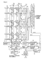
- the overall structure of an MRAM according to a first embodiment of the present invention is described with reference to Figs. 1 and 2.
- the MRAM according to the first embodiment is similar in structure to the conventional DRAM except a memory cell array.
- the MRAM is now specifically described.
- the MRAM according to the first embodiment is mainly formed by a matrix-shaped memory cell array 51.
- the memory cell array 51 is formed by memory cells 52 arranged in row and column directions. Each memory cell 52 stores 1-bit data forming the minimum unit of storage.
- each memory cell 52 is formed by two TMR elements 4a and 4b and two NMOS transistors 5a and 5b.
- the TMR element 4a includes a ferromagnetic layer 3a, an isolation barrier layer 2a and another ferromagnetic layer 1a harder to invert than the ferromagnetic layer 3a, as shown in Fig. 2.
- the TMR element 4b includes a ferromagnetic layer 3b, an isolation barrier layer 2b and another ferromagnetic layer 1b harder to invert than the ferromagnetic layer 3b.
- a word line WL is connected to the gates of the two NMOS transistors 5a and 5b.
- the TMR element 4a is an example of the "first storage element exhibiting a ferromagnetic tunnel effect" according to the present invention
- the TMR element 4b is an example of the "second storage element exhibiting a ferromagnetic tunnel effect” according to the present invention
- the ferromagnetic layers 3a and 3b are examples of the "first magnetic layer” according to the present invention
- the ferromagnetic layers 1a and 1b are examples of the "second magnetic layer” according to the present invention.
- the NMOS transistors 5a and 5b are examples of the “first transistor” and the "second transistor” according to the present invention respectively.
- the gates of the two NMOS transistors 5a and 5b are examples of the "control terminal" according to the present invention.
- each memory cell 52 arranged in the row direction is connected to the word line WL and a sub-word line SWL.
- Each memory cell 52 arranged in the column direction is connected to a bit line BL and an inverted bit line /BL.
- the inverted bit line /BL forms a pair of bit lines with the bit line BL corresponding thereto.
- Each pair of bit lines BL and /BL are connected to each cross-coupled latch type sense amplifier (SA) 53.
- SA cross-coupled latch type sense amplifier
- NMOS transistors 8a and 8b are provided between each pair of bit lines BL and /BL and each sense amplifier (SA) 53 for isolating each pair of bit lines BL and /BL from each sense amplifier (SA) 53.
- a signal line ⁇ 3 is connected to the gates of the NMOS transistors 8a and 8b.
- the NMOS transistors 8a and 8b are examples of the "isolation transistor" according to the present invention.
- the sense amplifier 53 is an example of the "amplifier” according to the present invention.
- Each word line WL is connected to a row decoder 54.
- An externally specified row address RA is supplied to the row decoder 64 from a row address buffer 55.
- the row decoder 54 selects the word line WL corresponding to the row address RA.
- a first end of the sub-word line SWL is connected to each word line WL through an inverter circuit including an NMOS transistor 6 and a PMOS transistor 7.
- a power supply potential Vcc is connected to a second end of the sub-word line SWL through a PMOS transistor 9.
- a signal line ⁇ 4 is connected to the gate of the PMOS transistor 9.
- the word line WL is connected to a first input terminal and an output terminal of an AND circuit 11.
- a signal line ⁇ 6 regularly reaching zero (low level) in writing is connected to a second input terminal of the AND circuit 11.
- NMOS transistors 10a and 10b are connected to the bit line BL and the inverted bit line /BL respectively.
- a signal line ⁇ 5 is connected to the gates of the NMOS transistors 10a and 10b.
- First ends of the NMOS transistors 10a and 10b are connected with each other.
- a precharge circuit 67 is connected to the interconnected NMOS transistors 10a and 10b.
- Each sense amplifier 53 is connected to an input/output line I/O and an inverted input/output line /I/O through each transfer gate 56.
- the input/output line I/O and the inverted input/output line /I/O form a pair of input/output lines I/O and /I/O.
- the pair of input/output lines I/O and /I/O are connected to a read amplifier 57.
- the read amplifier 57 is connected to a data output circuit 58 through a data bus DB and an inverted data bus /DB.
- the data bus DB and the inverted data bus /DB form a pair of data buses DB and /DB.
- a precharge circuit 59 is connected to the pair of input/output lines I/O and /I/O.
- the output circuit 58 outputs data.
- Each transfer gate 56 is connected to a column decoder 60 through a column selection line CSL.
- Each transfer gate 56 is formed by a pair of NMOS transistors connected between the pair of input/output lines I/O and /I/O and the sense amplifier 53.
- the gates of the pair of NMOS transistors are connected to the column decoder 60 through a single column selection line CSL. When the column selection line CSL goes high, therefore, the pair of NMOS transistors are turned on and the transfer gate 56 enters an ON state.
- An externally specified column address CA is supplied to the column decoder 60 and an address transition detector (ATD) 62 from a column address buffer 61.
- ATD address transition detector
- the ATD 62 detects change of the column address CA for detecting external specification of the column address CA, and generates a pulse signal ATD1. In other words, the ATD 62 generates the pulse signal ATD1 every time the column address CA changes.
- the pulse signal ATD1 is output to a column decoder control circuit 63, a precharge control circuit 64 and a read amplifier control circuit 65.
- the precharge control circuit 64 generates a one-pulse precharge circuit activation signal PC going high for a previously set time on the basis of fall of the pulse signal ATD1 from a high level to a low level.
- the activation signal PC is output to the precharge circuit 59.
- the precharge circuit 59 When activated, the precharge circuit 59 performs precharging for setting the pair of input/output lines I/O and /I/O to the same potential of a prescribed level (e.g., 1/2 Vcc (Vcc: driving voltage for the MRAM).
- a prescribed level e.g. 1/2 Vcc (Vcc: driving voltage for the MRAM).
- the precharge circuit 59 When receiving the activation signal PC, the precharge circuit 59 is inactivated (enters a standby state for activation) and stops precharging the pair of input/output lines I/O and /I/O.
- the column decoder control circuit 63 generates a one-pulse column decoder activation signal YS going high for a previously set time on the basis of fall of the pulse signal ATD1 from a high level to a low level.
- the activation signal YS is output to the column decoder 60.
- the column decoder 60 When receiving the activation signal YS, the column decoder 60 is activated and selects a column (a pair of bit lines BL and /BL) of the memory cell array 51 corresponding to the externally specified column address CA. In other words, the column decoder 60 is activated when receiving the activation signal YS. When activated, the column decoder 60 selects the column selection line CSL corresponding to the externally specified column address CA while converting the column selection line CSL to a high level. Thus, the transfer gate 56 connected to the column selection line CSL enters an ON state. Therefore, the column of the memory cell array 51 corresponding to the externally specified column address CA is selected through the sense amplifier 53 corresponding to the transfer gate 56.
- the read amplifier control circuit 65 generates a one-pulse read amplifier activation signal READ by delaying the pulse signal ATD1 by a prescribed time on the basis of fall of the pulse signal ATD1 from a high level to a low level.
- the timing and the pulse width of the activation signal READ are previously set.
- the activation signal READ is output to the read amplifier 57.
- the delay time for the activation signal READ is so set that the potential difference between the pair of input/output lines I/O and /I/O reaches a level sufficient for reading data.
- the delay time is set to a time for waiting for the pair of input/output lines I/O and /I/O changing from the precharged potentials to potentials exhibiting difference sufficient for preventing the read amplifier 57 from erroneous reading.
- control circuits 63 to 65 are provided with delay circuits and pulse generation circuits for generating the activation signals YS, PC and READ at proper timings and with proper pulse widths in response to the fall of the pulse signal ATD1 from a high level to a low level.
- the MRAM is further provided with a read detection circuit 66 detecting the potential difference between the pair of data buses DB and /DB and generating a read detection signal READ on the basis of the result of the detection.
- a read detection circuit 66 detects the read operation on the basis of the potential difference between the pair of data bus lines DB and /DB and generates the high-level read detection signal READ on the basis of the result of the detection. This detection signal READ is output to the column decoder control circuit 63, the precharge control circuit 64 and the read amplifier 65.
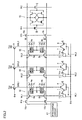
- Fig. 4 is a sectional block diagram showing the memory cell part of the MRAM according to the first embodiment shown in Figs. 1 and 2.
- the sectional structure of the memory cell 52 according to the first embodiment is now described with reference to Fig. 4.
- isolation regions 72 are formed on prescribed regions of a surface of a substrate 71.
- N-type source/drain regions 73 are formed on an element forming region enclosed with the isolation regions 72 at prescribed intervals.
- Gate electrodes forming word lines WL1 and WL2 are formed on channel regions located between the adjacent N-type source/drain regions 73.
- Each gate electrode and each pair of N-type source/drain regions 73 form each NMOS transistor 5a.
- the ferromagnetic layers 3a of the TMR elements 4a are connected to the N-type source/drain regions 73 located on both ends through conductive layers 74 and 75.
- the ferromagnetic layers 3a are easy to invert, and change the directions of magnetization in response to data as shown in Fig. 4.
- the ferromagnetic layers 1a harder to invert than the ferromagnetic layers 3a are formed on the other surfaces of the ferromagnetic layers 3a through the isolation barrier layers 2a.
- the ferromagnetic layers 1a are not inverted in response to the data but unidirectionally fixed.
- Sub-word lines SWL1 and SWL2 are connected to the ferromagnetic layers 1a through conductive layers 77.
- a bit line BL is connected to the central N-type source/drain region 73 through a conductive layer 76.
- An interlayer dielectric film 78 is formed between the bit line BL and the substrate 71.
- the memory cell 52 of the MRAM according to the first embodiment having the circuit structure shown in Figs. 1 and 2 can be readily implemented.
- the write operation is described with reference to a case of writing data in a memory cell 52 connected to the word line WL1.
- the signal line ⁇ 6 is set to a low level.
- a low-level signal is input in the second input terminal of the AND circuit 11.
- the word line WL1, selected by the row decoder 54, connected to the first input terminal of the AND circuit 11 is at a high level. Therefore, a part of the selected word line WL1 output from the AND circuit 11 goes low.
- the signal line ⁇ 6 is set to a low level thereby forcibly setting the word line WL1 connected to the output terminal of the AND circuit 11 to a low level.
- the NMOS transistors 5a and 5b connected to the word line WL1 connected to the output terminal of the AND circuit 11 enter OFF states.
- the signal line ⁇ 4 is converted to a low level, thereby turning on the PMOS transistor 9.
- the word line WL1 connected to the sub-word line SWL1 through the inverter circuit is at a high level, and hence the NMOS transistor 6 forming the inverter circuit enters an ON state.
- a lower part of the sub-word line SWL1 reaches a ground potential.
- An upper part of the sub-word line SWL1 reaches the power supply potential Vcc since the PMOS transistor 9 is turned on due to the fall of the signal line ⁇ 4, whereby a current flows to the sub-word line SWL1 downward from above.
- the selected bit line BL and the selected inverted bit line /BL are set to high and low levels respectively through the pair of input/output lines I/O and /I/O.
- the signal line ⁇ 5 is raised to a high level, thereby turning on the NMOS transistors 10a an 10b.
- the bit line BL and the inverted bit line /BL corresponding thereto are so shorted that a current flows from the high-level bit line BL to the low-level inverted bit line /BL.
- a leftward current flows to the bit line BL while a rightward current flows to the inverted bit line /BL.
- bit line BL and the inverted bit line /BL In order to reverse the directions of the currents flowing to the bit line BL and the inverted bit line /BL, low- and high-level signals are supplied to the bit line BL and the inverted bit line /BL respectively.
- inverted data (1" and "0", for example) can be readily written in the ferromagnetic layers 3a and 3b of the TMR elements 4a and 4b of the selected memory cell 52 by feeding a current to the subword line SWL1 downward from above while feeding currents of opposite directions to the pair of bit lines BL and /BL in the selected memory cell 52.
- the directions of the currents fed to the bit line BL and the inverted bit line /BL may be reversed.
- the word line WL1 Before rising, the word line WL1 is at a low level. In this case, the PMOS transistor 7 of the inverter circuit connected to the word line WL1 enters an ON state, whereby the potential of the sub-word line SW1 reaches the power supply potential Vcc. Thus, the potential of a node a also reaches the power supply potential Vcc. Further, the potentials of the TMR elements 4a and 4b, which are conductors, also reach the power supply potential Vcc. In this state, the signal line ⁇ 5 is raised to a high level while the precharge circuit 67 precharges the bit line BL and the inverted bit line /BL to the power supply potential Vcc.
- the NMOS transistors 5a and 5b connected to the word line WL1 set to a high level by the row decoder 54 enter ON states.
- the bit line BL and the inverted bit line /BL as well as the TMR elements 4a and 4b are rendered conductive.
- the potentials of the bit line BL, the inverted bit line /BL and the node a are at the power supply potential Vcc.
- the signal line ⁇ 5 goes low to disconnect the precharge circuit 67 while the NMOS transistor 6 forming the inverter circuit connected to the word line WL1 enters an ON state, whereby the potential of the sub-word line SWL1 is gradually lowered toward a ground potential GND.
- the potential of the node a is also gradually lowered to the ground potential GND. Therefore, the potentials of the bit line BL and the inverted bit line /BL are also gradually lowered to the ground potential GND.
- the resistance of the TMR element 4a, having the upper and lower ferromagnetic layers 3a and 1a forming magnetic fields in opposite directions, connected to the bit line BL is slightly higher than that of the TMR element 4b connected to the inverted bit line /BL.
- bit line BL and the inverted bit line /BL are started to be lowered toward the ground potential GND, the bit line BL and the inverted bit line /BL and the node a are only slightly different in potential from each other, and hence the MR ratio (rate of resistance change) is maximized.
- the potentials of the bit line BL and the inverted bit line /BL are also lowered.
- the potential of the TMR element 4a, having slightly higher resistance, connected to the bit line BL is lowered more slowly as compared with the inverted bit line /BL.
- potential difference is caused between the bit line BL and the inverted bit line /BL.
- the word line WL1 is lowered from a high level to a low level at the timing of this potential difference, as shown in Fig. 3.
- This fall timing of the word line WL1 is set before the potential of the node a reaches the ground potential GND for the following reason:
- the potential difference between the bit line BL and the inverted bit line /BL is caused only in a transient state.
- the potentials of the ferromagnetic layers 1a and 1b (the potential of the node a ) of the TMR elements 4a and 4b reach the ground potential GND, therefore, the potentials of the bit line BL and the inverted bit line /BL connected to the ferromagnetic layers 3a and 3b respectively also reach the ground potential GND. In this case, the potential difference between the bit line BL and the inverted bit line /BL disappears to disable detection.
- the TMR elements 4a and 4b While potential difference is caused between the bit line BL and the inverted bit line /BL at a transient timing, the TMR elements 4a and 4b are conductors and hence the bit line BL and the inverted bit line /BL finally reach the same potential. Therefore, the signal line ⁇ 3 is lowered in response to the fall timing of the word line WL1.
- the NMOS transistors (isolation transistors) 8a and 8b enter OFF states, for isolating the bit line BL and the inverted bit line /BL from the sense amplifier 53. Thereafter the signal lines ⁇ 1 and ⁇ 2 of the sense amplifier 53 are raised thereby activating the sense amplifier 53.
- the potential difference between the bit line BL and the inverted bit line /BL connected to the sense amplifier 53 is amplified so that the potentials of the bit line BL and the inverted bit line /BL reach the power supply potential Vcc and the ground potential GND respectively.
- the data is read.
- the signal line ⁇ 5 is lowered and the precharge circuit 67 is turned on for precharging the bit line BL and the inverted bit line /BL to the power supply potential Vcc.
- data can be readily read by forming each memory cell 52 by the two TMR elements 4a and 4b and the two NMOS transistors 5a and 5b while detecting the potential difference between the bit line BL and the inverted bit line /BL connected to the two TMR elements 4a and 4b through the sense amplifier 53.
- the potential difference is so detected that no value of a small current flowing to the bit line BL may be detected dissimilarly to the conventional memory cell formed by a single TMR element and a single NMOS transistor. Consequently, the sense amplifier 53 may not have a complicated structure for detecting the value of a small current.
- data stored in the MRAM can be read through the simple sense amplifier 53 similar to that employed in a conventional DRAM by detecting the potential difference between the bit line BL and the inverted bit line /BL through the sense amplifier 53, as hereinabove described.
- the data can be read through the simple sense amplifier 53, whereby high-speed reading is enabled as compared with the prior art employing a sense amplifier having a complicated structure.
- the structure of the sense amplifier 53, the overall circuit structure and the operating method are similar to those in the conventional DRAM, whereby the technique of the DRAM can be utilized as such. Consequently, replacement from the DRAM is simplified.
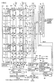
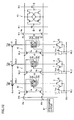
- an MRAM according to a second embodiment of the present invention is different from the MRAM according to the first embodiment shown in Figs. 1 and 2 in a point that a dummy bit line (dummy BL) as well as a comparator 201 for detecting the potential of the dummy bit line are provided.
- the comparator 201 is an example of the "detection circuit" according to the present invention.
- the dummy bit line (dummy BL) similar in structure to a bit line BL is provided as shown in Figs. 5 and 6.
- TMR elements 4a are connected to the dummy bit line through transistors 5a. All TMR elements 4a connected to the dummy bit line are so set that ferromagnetic layers 1a an 3a have the same (parallel) directions of magnetization.
- the dummy bit line is connected to a first input end of the comparator 201.
- a reference voltage Vcc is connected to a second input end of the comparator 201.
- An inverter 202 is connected to an output of the comparator 201, while another inverter 203 is connected to an output of the inverter 202.
- the output of the inverter 202 is employed as a signal ⁇ 1, while the output of the inverter 203 is employed as a signal ⁇ 2.
- the signals ⁇ 1 and ⁇ 2 are employed as activation signals for sense amplifiers 53.
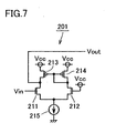
- the comparator 201 includes a pair of PMOS transistors 213 and 214, an NMOS transistor 211 having a gate receiving an input voltage (the voltage of the dummy bit line) Vin and an NMOS transistor 212 having a gate receiving the reference voltage Vcc.
- the NMOS transistor 211 is an example of the "first transistor” according to the present invention
- the NMOS transistor 212 is an example of the "second transistor” according to the present invention.
- a constant current source 215 is connected to first terminals of the NMOS transistors 211 and 212.
- the reference voltage Vcc is connected to first terminals of the PMOS transistors 213 and 214.
- a node between second terminals of the PMOS transistor 213 and the NMOS transistor 211 outputs an output voltage Vout.
- the comparator 201 is so structured that the quantity of a current flowing to the NMOS transistor 211 receiving the input voltage Vin is larger than that of a current flowing to the NMOS transistor 212 receiving the reference voltage Vcc. More specifically, the gate width of the NMOS transistor 211 is rendered slightly larger than that of the NMOS transistor 212, thereby increasing the quantity of the current flowing to the NMOS transistor 211 beyond that of the current flowing to the NMOS transistor 211. It is also possible to increase the quantity of the current flowing to the NMOS transistor 211 beyond that of the current flowing to the NMOS transistor 212 by reducing the gate length of the NMOS transistor 211 slightly below that of the NMOS transistor 211 without changing the gate widths.
- the quantity of the current flowing to the MOS transistor 211 receiving the input voltage Vin is rendered larger than that of the current flowing to the NMOS transistor 212 receiving the reference voltage Vcc, so that a low-level signal can be output as the output voltage Vout also when the input voltage Vin is identical to the reference voltage Vcc.
- the output of the comparator 201 can be prevented from being undefined when the input voltage Vin for the comparator 201 is identical to the reference voltage Vcc.
- the comparator 201 according to the second embodiment outputs a low-level signal when the input voltage Vin is identical to the reference voltage Vcc, while outputting a high-level signal when the input voltage Vin is lower than the reference voltage Vcc.
- a signal ⁇ 7 and an output of a column decoder 60 are input in an AND circuit 205, as shown in Figs. 5 and 6.
- An output of the AND circuit 205 is connected to the gate of a transistor 204 for connecting the bit line BL with an inverted bit line /BL. According to this structure, only a selected bit line BL and the inverted bit line /BL corresponding thereto can be readily shorted.
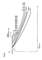
- Fig. 8 is an operation waveform conceptual diagram for illustrating the read operation of the MRAM according to the second embodiment of the present invention.
- Figs. 9 and 10 are operation waveform simulation diagrams for illustrating the read operation of the MRAM according to the second embodiment.
- the read operation according to the second embodiment is described with reference to such a case that the resistance of the TMR element 4a connected to the bit line BL is lower than that of the TMR element 4b connected to the inverted bit line /BL.
- the TMR element 4a is magnetized in the same direction (parallel) and the TMR element 4b is magnetized in opposite directions (antiparallel) as in the memory cell 52 connected to a word line WL2 shown in Fig. 6.
- the read operation is now described on the assumption that the word line WL2 is selected.
- the word line WL2 is at a low level in an initial state before rising.
- a PMOS transistor 7 of an inverter circuit connected to the word line WL2 enters an ON state, whereby the potential of a sub-word line SWL2 reaches the reference voltage Vcc.
- the potential of a node a also reaches the reference voltage Vcc.
- the potentials of the TMR elements 4a and 4b, which are conductors, also reach the reference voltage Vcc.
- a signal ⁇ 5 is raised to a high level while a precharge circuit 67 precharges the bit line BL and the inverted bit line /BL as well as the dummy bit line to the reference voltage Vcc.
- bit line BL and the inverted bit line /BL as well as the TMR elements 4a and 4b are rendered conductive.
- the potentials of the bit line BL, the inverted bit line /BL, the dummy bit line (dummy BL), the node a and nodes b and c are at the reference voltage Vcc.
- the signal ⁇ 5 goes low to disconnect the precharge circuit 67 while an NMOS transistor 6 of the inverter circuit connected to the word line WL2 enters an ON state, whereby the potential of the sub-word line SWL2 is gradually lowered toward a ground potential GND.
- the potential of the node a is also gradually reduced toward the ground potential GND. Therefore, the potentials of the bit line BL and the inverted ⁇ bit line /BL are also gradually reduced to the ground potential GND.
- Fig. 8 shows waveforms in the case of raising the word line WL and gradually lowering the sub-word line SWL.
- the word line WL rises and the sub-word line SWL gradually falls so that the nodes b and c (see Fig. 6) fall.
- the TMR element 4a having the same direction (parallel) of magnetization and the TMR element 4b having opposite directions (antiparallel) of magnetization exhibit different resistance values, to cause potential difference between the nodes b and c.
- the bit line BL and the inverted bit line /BL on a cell side start to fall when the potentials of the nodes b and c are reduced below Vcc - Vt (threshold voltage).
- Vcc - Vt threshold voltage
- the potential of the TMR element 4a having the parallel direction of magnetization and exhibiting lower resistance starts to lower in advance of that of the TMR element 4b having antiparallel directions of magnetization and exhibiting higher resistance.
- On-state resistance of the transistors 5a and 5b connected to the bit line BL and the inverted bit line /BL on the cell side depend on gate-to-source potential difference VgsB and VgsC (see Fig. 6) of the transistors 5a and 5b.
- VgsB and VgsC see Fig. 6
- the potentials of the nodes b and c are different from each other, and hence the gate-to-source potential difference VgsB of the transistor 5a is different from the gate-to-source potential difference VgsC of the transistor 5b. Therefore, the transistor 5a connected to the TMR element 4a having lower resistance (parallel direction of magnetization) is increased in potential difference Vgs and reduced in resistance.
- the potential difference between the bit line BL and the inverted bit line /BL on the cell side exceeds the potential difference between the nodes b and c.
- the potential difference (Vsig) between a bit line BL and an inverted bit line /BL on the side of the sense amplifier 53 is increased due to influence by potential difference Vgs of isolation NMOS transistors 8a and 8b.
- wiring capacities of the bit line BL and the inverted bit line /BL on the side of the sense amplifier 53 are smaller than those of the bit line BL and the inverted bit line /BL on the cell side, and hence the bit line BL and the inverted bit line /BL on the side of the sense amplifier 53 reach the same potentials as the bit line BL and the inverted bit line /BL on the cell side. Therefore, potential difference input across the sense amplifier 53 can be set large from a timing when the potentials of the bit line BL and the inverted bit line /BL on the side of the sense amplifier 53 start to lower from the reference voltage Vcc to a timing when the same reach the same potentials as the bit line BL and the inverted bit line /BL on the cell side.
- the sense amplifier 53 starts detection at an arbitrary timing before the potentials of the bit line BL and the inverted bit line /BL on the cell side reach 0 V. In this case, there is a possibility of missing a timing efficient for detection.
- the dummy bit line (dummy BL) and the comparator 201 for detecting the potential of the dummy bit line are provided thereby detecting the fall timing of the bit line BL on the side of the sense amplifier 53.
- the bit line BL and the inverted bit line /BL on the cell side are isolated from the bit line BL and the inverted bit line /BL on the side of the sense amplifier 53 at this timing for operating the sense amplifier 53.
- the potentials of the bit line BL and the inverted bit line /BL, the dummy bit line (dummy BL) and the sub-word line SWL2 are at the reference voltage Vcc in an initial state, as described above. Thereafter the word line WL2 rises while the sub-word line SWL starts to gradually fall. Thus, potential difference is caused between the bit line BL and the inverted bit line /BL on the cell side.
- the potentials of the bit line BL and the inverted bit line /BL on the cell side thereafter fall below Vcc - Vt, the potentials of the bit line BL and the inverted bit line /BL on the side of the sense amplifier 53 start to fall from the reference voltage Vcc, as shown in Fig. 8.
- the potential of the dummy bit line (on the side of the comparator 201) also starts to lower at this timing.
- the TMR element 4a connected to the dummy bit line is set in the state of the parallel direction of magnetization with low resistance, and hence the potential of the dummy bit line starts to lower at the same timing as either the bit line BL or the inverted bit line /BL (the bit line BL in the second embodiment) having lower resistance.
- an input Vin of the comparator 201 connected with the dummy bit line is identical to the reference voltage Vcc.
- a low-level signal is output as an output Vout in the second embodiment.
- the comparator 201 at the level of the reference voltage Vcc outputs a high-level signal.
- the signal ⁇ 2 goes high and the signal ⁇ 1 goes low.
- the sense amplifier 53 is activated. Further, the signal ⁇ 3 falls at this timing.
- the isolation NMOS transistors 8a and 8b enter OFF states, thereby isolating the bit line BL and the inverted bit line /BL on the cell side from the bit line BL and the inverted bit line /BL on the side of the sense amplifier 53.
- bit line BL and the inverted bit line /BL on the side of the sense amplifier 53 are amplified and read similarly to sensing of a DRAM.
- the bit line BL and the inverted bit line /BL on the cell side return to the initial state due to the signal ⁇ 5 going high.
- Figs. 9 and 10 show actual simulation waveforms.
- Fig. 9 shows waveforms obtained by observing only the behavior of the bit lines BL without starting sensing by the sense amplifier 53.
- Fig. 10 shows waveforms obtained by operating the sense amplifier 53 by driving the comparator 201.
- the write operation according to the second embodiment is basically identical to the aforementioned write operation according to the first embodiment, and hence redundant description is not repeated.
- the signal ⁇ 7 and the output of the column decoder 60 are input in the AND circuit 205 while the output of the AND circuit 205 is connected to the gate of the transistor 204 for connecting the bit line BL and the inverted bit line /BL, as described above.
- the selected bit line BL and the inverted bit line /BL corresponding thereto can be readily shorted in the write operation.
- the fall timing of the bit line BL on the side of the sense amplifier 53 can be detected through the dummy bit line and the comparator 201. Further, the sense amplifier 53 can readily detect the potential difference (Vsig) between the bit line BL and the inverted bit line /BL on the side of the sense amplifier 53 by turning off the isolation NMOS transistors 8a and 8b and activating the sense amplifier 53 at the fall timing of the dummy bit line detected by the comparator 201.
- Vsig potential difference
- an MRAM according to a third embodiment of the present invention is different from the MRAM according to the first embodiment shown in Figs. 1 and 2 only in a memory cell part.
- each memory cell 82 is formed by a double junction TMR element 24 and two NMOS transistors 5a and 5b.
- the circuit structure of the third embodiment is similar to that of the first embodiment except the memory cell part.
- the double junction TMR element 24 includes a ferromagnetic layer 23a, an isolation barrier layer 22a, another ferromagnetic layer 23b, another isolation barrier layer 22b and still another ferromagnetic layer 21 harder to invert than the ferromagnetic layers 23a and 23b.
- the ferromagnetic layers 23a and 23b are formed on both surfaces of the central ferromagnetic layer 21, which is harder to invert, through the isolation barrier layers 22a and 22b respectively.
- the ferromagnetic layer 21 shown in Fig. 12 share the ferromagnetic layers 1a and 1b of the TMR elements 4a and 4b according to the first embodiment shown in Fig. 2.
- the double junction TMR element 24 according to the third embodiment can have the same functions as the two TMR elements 4a and 4b according to the first embodiment.
- the double junction TMR element 24 is an example of the "storage element exhibiting a ferromagnetic tunnel effect" according to the present invention.
- the ferromagnetic layer 23a is an example of the "first magnetic layer” according to the present invention
- the ferromagnetic layer 21 is an example of the “second magnetic layer” according to the present invention
- an the ferromagnetic layer 23b is an example of the "third magnetic layer” according to the present invention.
- the isolation barrier layer 22a is an example of the "first isolation barrier layer” according to the present invention
- the isolation barrier layer 22b is an example of the "second isolation barrier layer” according to the present invention.
- the double junction TMR element 24 simply substitutes for the two TMR elements 4a and 4b according to the first embodiment as described above, while the remaining circuit structure is similar to that of the first embodiment. Therefore, write and read operations of the MRAM according to the third embodiment are also similar to those of the MRAM according to the first embodiment. Therefore, redundant description is not repeated.
- each memory cell 82 is formed by the double junction TMR element 24 including the ferromagnetic layers 21, 23a and 23b and the isolation barrier layers 22a and 22b and two NMOS transistors 5a and 5b, whereby the area of the memory cell 82 can be reduced as compared with the memory cell 52 according to the first embodiment formed by the two TMR elements 4a and 4b and the two NMOS transistors 5a and 5b.
- the MRAM according to the third embodiment performing a read operation similar to that of the MRAM according to the first embodiment, can attain an effect similar to that of the first embodiment.
- data can be readily read by detecting potential difference between a bit line BL and an inverted bit line /BL connected to the double TMR element 24 through a sense amplifier 53 (see Fig. 12).
- a sense amplifier 53 see Fig. 12
- no value of a small current flowing to the bit line BL may be detected dissimilarly to the conventional memory cell formed by a single TMR element and a single NMOS transistor. Consequently, the sense amplifier 53 may not have a complicated structure for detecting the value of a small current.
- the MRAM according to the third embodiment is so structured as to detect the potential difference between the bit line BL and the inverted bit line /BL through the sense amplifier 53 (see Fig. 12) similarly to the aforementioned first embodiment, whereby data stored in the MRAM can be read through the simple sense amplifier 53 similar to that employed for a conventional DRAM.
- data can be read through the simple sense amplifier 53, whereby high-speed reading is enabled as compared with the prior art employing a sense amplifier having a complicated structure.
- the structure of the sense amplifier 53, the overall circuit structure and an operating method are similar to those of the conventional DRAM similarly to the first embodiment, whereby the technique of the DRAM can be utilized as such. Consequently, replacement from a DRAM is simplified. Further, data can be readily detected also when the double junction TMR element 24 has high resistance by reading the potential difference caused between the bit line BL and the inverted bit line /BL by inputting a pulse signal in a selected word line through the sense amplifier 53 (Fig. 12), dissimilarly to the conventional case of reading the value of a small current.
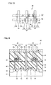
- Fig. 13 is a plane layout diagram for implementing the circuit structure of the MRAM according to the third embodiment shown in Figs. 11 and 12, and Fig. 14 is a sectional view taken along the line 100-100 in Fig. 13.
- the structure of the memory cell 82 of the MRAM according to the third embodiment is now described with reference to Figs. 13 and 14.
- the plane layout diagram of Fig. 13 shows only the bit line BL and the inverted bit line /BL, the ferromagnetic layers 21, 23a and 23b forming the double junction TMR element 24 and a bit line contact part 94, in order to simplify the illustration.
- isolation regions 92 are formed on prescribed regions of a surface of a substrate 91, as shown in Fig. 14.
- N-type source/drain regions 93 are formed on an element forming region enclosed with the isolation regions 92 at prescribed intervals.
- Gate electrodes forming word lines WL1 and WL2 are formed on channel regions located between the adjacent N-type source/drain regions 93.
- the readily inverted sidewall-shaped ferromagnetic layers 23a of the double junction TMR elements 24 are connected to the N-type source/drain regions 93 located on both ends through conductive layers 96.
- the conductive layers 96 and the ferromagnetic layers 23a are connected with each other through contact holes 99.
- barrier films (not shown) may be formed between the conductive layers 96 and the ferromagnetic layers 23a.
- the hardly inverted ferromagnetic layers 21 are formed on side surfaces of the ferromagnetic layers 23a through the isolation barrier layers 22a.
- the readily inverted sidewall-shaped ferromagnetic layer 23b are formed on other side surfaces of the ferromagnetic layers 21 through the isolation barrier layers 22b.
- the ferromagnetic layers 23a and 23b of the double junction TMR elements 24 are formed in a staggered manner with respect to the central ferromagnetic layers 21, as shown in Fig. 13.
- the bit line BL is connected to the bit line contact part 94 located on the surface of the central N-type source/drain region 93 through a conductive layer 98.
- Interlayer dielectric films 95 and 97 are formed to cover the overall surface.
- Figs. 15 to 17 are sectional views and a perspective view for illustrating a process of fabricating the double junction TMR element part shown in Figs. 13 and 14. The fabrication process for the double junction TMR element part is now described with reference to Figs. 15 to 17.
- the ferromagnetic layer 21 patterned in a prescribed shape is formed on the interlayer dielectric film 95, as shown in Fig. 15.
- An alumina layer 22 is formed as an isolation barrier material layer to cover the ferromagnetic layer 21 and the interlayer dielectric film 95, and thereafter the contact hole 99 is formed in a region of the alumina layer 22 located on the conductive layer 96. Thereafter a ferromagnetic material layer 23 is formed on the overall surface. The overall surface is anisotropically etched thereby forming the sidewall-shaped ferromagnetic layers 23a and 23b as shown in Fig. 16. In this case, the ferromagnetic layer 23a, formed also in the contact hole 99, is electrically connected with the conductive layer 96.
- the double junction TMR element 24 consisting of the ferromagnetic layers 21, 23a and 23b can be readily formed through a process similar to a conventional sidewall forming process, as hereinabove described.
- multilayer films consisting of Co 75 -Fe 25 layers, Py layers and Ta layers are employed for the readily inverted ferromagnetic layers 23a and 23b, while a multilayer film consisting of a Co 75 -Fe 25 layer, an Ir-Mn layer, a Py layer, a Cu layer, a Py layer and a Ta layer is employed for the hardly inverted ferromagnetic layer 21, for example.
- These materials for the ferromagnetic layers are disclosed in page 5, "Present Circumstances and Future Prospects of MRAM and Competitive Techniques" (November 17, 2000), Data of the 116 th Meeting of the Magnetic Society of Japan.
- the double junction TMR elements 24 shown in Figs. 13 and 14 can be readily formed.
- each of the aforementioned embodiments employs the TMR element as the storage element forming each memory cell
- the present invention is not restricted to this but a storage element other than the TMR element can also be employed so far as the same exhibits a ferromagnetic tunnel effect. Further, an effect similar to those of the aforementioned embodiments can be attained also when employing a storage element exhibiting a magnetic resistance effect in place of the storage element exhibiting a ferromagnetic tunnel effect.
- the present invention is not restricted to this but a similar effect can be attained also when adding the dummy bit line (dummy BL) and the comparator 201 to the structure of the third embodiment including the memory cell 82.
Landscapes
- Engineering & Computer Science (AREA)
- Computer Hardware Design (AREA)
- Mram Or Spin Memory Techniques (AREA)
- Hall/Mr Elements (AREA)
- Semiconductor Memories (AREA)
Applications Claiming Priority (4)
| Application Number | Priority Date | Filing Date | Title |
|---|---|---|---|
| JP2000341489 | 2000-11-09 | ||
| JP2000341489 | 2000-11-09 | ||
| JP2000399990 | 2000-12-28 | ||
| JP2000399990 | 2000-12-28 |
Publications (2)
| Publication Number | Publication Date |
|---|---|
| EP1205937A2 true EP1205937A2 (fr) | 2002-05-15 |
| EP1205937A3 EP1205937A3 (fr) | 2003-04-09 |
Family
ID=26603635
Family Applications (1)
| Application Number | Title | Priority Date | Filing Date |
|---|---|---|---|
| EP01309423A Withdrawn EP1205937A3 (fr) | 2000-11-09 | 2001-11-06 | Dispositif de mémoire magnétique avec des cellules de mémoire ferromagnétiques à effet tunnel |
Country Status (5)
| Country | Link |
|---|---|
| US (1) | US6549455B2 (fr) |
| EP (1) | EP1205937A3 (fr) |
| KR (1) | KR100447769B1 (fr) |
| CN (1) | CN1226747C (fr) |
| TW (1) | TW584976B (fr) |
Cited By (3)
| Publication number | Priority date | Publication date | Assignee | Title |
|---|---|---|---|---|
| US7116595B2 (en) | 2001-05-16 | 2006-10-03 | Renesas Technology Corp. | Thin film magnetic memory device having a magnetic tunnel junction |
| CN100424783C (zh) * | 2002-09-03 | 2008-10-08 | 三星电子株式会社 | 每个存储单元具有多位的磁存储器件 |
| EP2601655B1 (fr) * | 2010-08-03 | 2019-01-02 | Qualcomm Incorporated(1/3) | Création d'un état non réversible dans une cellule binaire ayant une première jonction à effet tunnel magnétique et une seconde jonction à effet tunnel magnétique |
Families Citing this family (23)
| Publication number | Priority date | Publication date | Assignee | Title |
|---|---|---|---|---|
| KR100451096B1 (ko) * | 2000-09-19 | 2004-10-02 | 엔이씨 일렉트로닉스 가부시키가이샤 | 자기메모리셀어레이를 갖는 비휘발성 반도체메모리장치 |
| JP2003151260A (ja) * | 2001-11-13 | 2003-05-23 | Mitsubishi Electric Corp | 薄膜磁性体記憶装置 |
| US6795336B2 (en) * | 2001-12-07 | 2004-09-21 | Hynix Semiconductor Inc. | Magnetic random access memory |
| JP3778100B2 (ja) * | 2002-02-08 | 2006-05-24 | ソニー株式会社 | 強磁性トンネル接合素子を用いた磁気記憶装置 |
| JP4047615B2 (ja) * | 2002-04-03 | 2008-02-13 | 株式会社ルネサステクノロジ | 磁気記憶装置 |
| JP2003303942A (ja) * | 2002-04-12 | 2003-10-24 | Mitsubishi Electric Corp | 半導体記憶装置 |
| KR100505104B1 (ko) * | 2002-04-30 | 2005-07-29 | 삼성전자주식회사 | 자기 램 셀들, 그 구조체들 및 그 구동방법 |
| JP2004013961A (ja) * | 2002-06-04 | 2004-01-15 | Mitsubishi Electric Corp | 薄膜磁性体記憶装置 |
| JP4399211B2 (ja) * | 2002-12-21 | 2010-01-13 | 株式会社ハイニックスセミコンダクター | バイオセンサー |
| JP4294307B2 (ja) * | 2002-12-26 | 2009-07-08 | 株式会社ルネサステクノロジ | 不揮発性記憶装置 |
| US6714442B1 (en) * | 2003-01-17 | 2004-03-30 | Motorola, Inc. | MRAM architecture with a grounded write bit line and electrically isolated read bit line |
| JP4283011B2 (ja) * | 2003-03-13 | 2009-06-24 | Tdk株式会社 | 磁気メモリデバイスおよびその読出方法 |
| JP4365604B2 (ja) | 2003-03-24 | 2009-11-18 | Tdk株式会社 | 磁気メモリデバイスおよびセンスアンプ回路、ならびに磁気メモリデバイスの読出方法 |
| US6888771B2 (en) * | 2003-05-09 | 2005-05-03 | Micron Technology, Inc. | Skewed sense AMP for variable resistance memory sensing |
| JP4646636B2 (ja) * | 2004-02-20 | 2011-03-09 | ルネサスエレクトロニクス株式会社 | 半導体装置 |
| JP2006031795A (ja) * | 2004-07-14 | 2006-02-02 | Renesas Technology Corp | 不揮発性半導体記憶装置 |
| US7339813B2 (en) * | 2004-09-30 | 2008-03-04 | Sharp Laboratories Of America, Inc. | Complementary output resistive memory cell |
| US7292467B2 (en) * | 2005-04-22 | 2007-11-06 | Taiwan Semiconductor Manufacturing Company, Ltd. | Magnetic random access memory device |
| US7474569B2 (en) * | 2006-05-25 | 2009-01-06 | Honeywell International Inc. | Two-element magnetic memory cell |
| JP2010177624A (ja) * | 2009-02-02 | 2010-08-12 | Toshiba Corp | 半導体記憶装置 |
| US9299410B2 (en) * | 2013-09-04 | 2016-03-29 | Shintaro SAKAI | Reading magnetic memory based on regions within a cell array |
| CN107430889B (zh) * | 2015-03-27 | 2020-09-01 | 松下半导体解决方案株式会社 | 半导体存储装置的改写方法以及半导体存储装置 |
| JP2019164848A (ja) * | 2018-03-19 | 2019-09-26 | 東芝メモリ株式会社 | 磁気記憶装置 |
Family Cites Families (6)
| Publication number | Priority date | Publication date | Assignee | Title |
|---|---|---|---|---|
| CA2060835A1 (fr) * | 1991-02-11 | 1992-08-12 | Romney R. Katti | Memoire vive analogique rapide remanente en circuit integre |
| US5343422A (en) * | 1993-02-23 | 1994-08-30 | International Business Machines Corporation | Nonvolatile magnetoresistive storage device using spin valve effect |
| JPH0863962A (ja) | 1994-08-29 | 1996-03-08 | Sanyo Electric Co Ltd | 記憶装置及び半導体記憶装置 |
| JPH09293387A (ja) | 1996-02-29 | 1997-11-11 | Sanyo Electric Co Ltd | 半導体メモリ |
| US5946227A (en) * | 1998-07-20 | 1999-08-31 | Motorola, Inc. | Magnetoresistive random access memory with shared word and digit lines |
| US6111781A (en) * | 1998-08-03 | 2000-08-29 | Motorola, Inc. | Magnetic random access memory array divided into a plurality of memory banks |
-
2001
- 2001-10-25 TW TW090126458A patent/TW584976B/zh not_active IP Right Cessation
- 2001-11-06 US US09/985,770 patent/US6549455B2/en not_active Expired - Lifetime
- 2001-11-06 EP EP01309423A patent/EP1205937A3/fr not_active Withdrawn
- 2001-11-09 KR KR10-2001-0069676A patent/KR100447769B1/ko not_active Expired - Fee Related
- 2001-11-09 CN CNB011378751A patent/CN1226747C/zh not_active Expired - Fee Related
Cited By (3)
| Publication number | Priority date | Publication date | Assignee | Title |
|---|---|---|---|---|
| US7116595B2 (en) | 2001-05-16 | 2006-10-03 | Renesas Technology Corp. | Thin film magnetic memory device having a magnetic tunnel junction |
| CN100424783C (zh) * | 2002-09-03 | 2008-10-08 | 三星电子株式会社 | 每个存储单元具有多位的磁存储器件 |
| EP2601655B1 (fr) * | 2010-08-03 | 2019-01-02 | Qualcomm Incorporated(1/3) | Création d'un état non réversible dans une cellule binaire ayant une première jonction à effet tunnel magnétique et une seconde jonction à effet tunnel magnétique |
Also Published As
| Publication number | Publication date |
|---|---|
| EP1205937A3 (fr) | 2003-04-09 |
| US20020054500A1 (en) | 2002-05-09 |
| CN1353422A (zh) | 2002-06-12 |
| KR20020042754A (ko) | 2002-06-07 |
| TW584976B (en) | 2004-04-21 |
| US6549455B2 (en) | 2003-04-15 |
| CN1226747C (zh) | 2005-11-09 |
| KR100447769B1 (ko) | 2004-09-08 |
Similar Documents
| Publication | Publication Date | Title |
|---|---|---|
| US6549455B2 (en) | Magnetic memory device including storage element exhibiting ferromagnetic tunnel effect | |
| JP3768143B2 (ja) | 磁気メモリ装置 | |
| US6903963B2 (en) | Thin-film magnetic memory device executing data writing with data write magnetic fields in two directions | |
| US6873561B2 (en) | Semiconductor memory device operating with low current consumption | |
| US7295465B2 (en) | Thin film magnetic memory device reducing a charging time of a data line in a data read operation | |
| US7116595B2 (en) | Thin film magnetic memory device having a magnetic tunnel junction | |
| US6757191B2 (en) | Thin film magnetic memory device sharing an access element by a plurality of memory cells | |
| US6822897B2 (en) | Thin film magnetic memory device selecting access to a memory cell by a transistor of a small gate capacitance | |
| US6822895B2 (en) | Magnetic memory device | |
| KR20030051193A (ko) | 레퍼런스셀 없이 데이터 판독을 실행하는 박막 자성체기억장치 | |
| US6903965B2 (en) | Thin film magnetic memory device permitting high precision data read | |
| US6760244B2 (en) | Magnetic memory device including storage elements exhibiting a ferromagnetic tunnel effect | |
| KR20030075960A (ko) | 자기 저항 램 | |
| KR100521363B1 (ko) | 마그네틱 랜덤 액세스 메모리의 데이터 센싱 회로 및 그방법 | |
| US7203088B2 (en) | Magnetoresistive random access memory and driving method thereof | |
| KR20030002257A (ko) | 자기저항램과 그의 셀 및 셀 어레이 | |
| JP2003297071A (ja) | 記憶装置 | |
| KR100516691B1 (ko) | 자기저항 램 | |
| KR100772797B1 (ko) | 자기저항램과 그의 셀 및 셀 어레이 | |
| KR100513369B1 (ko) | 자기저항 램 |
Legal Events
| Date | Code | Title | Description |
|---|---|---|---|
| PUAI | Public reference made under article 153(3) epc to a published international application that has entered the european phase |
Free format text: ORIGINAL CODE: 0009012 |
|
| AK | Designated contracting states |
Kind code of ref document: A2 Designated state(s): AT BE CH CY DE DK ES FI FR GB GR IE IT LI LU MC NL PT SE TR |
|
| AX | Request for extension of the european patent |
Free format text: AL;LT;LV;MK;RO;SI |
|
| PUAL | Search report despatched |
Free format text: ORIGINAL CODE: 0009013 |
|
| AK | Designated contracting states |
Kind code of ref document: A3 Designated state(s): AT BE CH CY DE DK ES FI FR GB GR IE IT LI LU MC NL PT SE TR Designated state(s): AT BE CH CY DE DK ES FI FR GB GR IE IT LI LU MC NL PT SE TR |
|
| AX | Request for extension of the european patent |
Extension state: AL LT LV MK RO SI |
|
| 17P | Request for examination filed |
Effective date: 20030618 |
|
| AKX | Designation fees paid |
Designated state(s): DE FR GB |
|
| STAA | Information on the status of an ep patent application or granted ep patent |
Free format text: STATUS: THE APPLICATION HAS BEEN WITHDRAWN |
|
| 18W | Application withdrawn |
Effective date: 20060927 |