EP1209512A1 - Reflektierende Flüssigkristallanzeige mit verbessertem Kontrast - Google Patents
Reflektierende Flüssigkristallanzeige mit verbessertem Kontrast Download PDFInfo
- Publication number
- EP1209512A1 EP1209512A1 EP00204224A EP00204224A EP1209512A1 EP 1209512 A1 EP1209512 A1 EP 1209512A1 EP 00204224 A EP00204224 A EP 00204224A EP 00204224 A EP00204224 A EP 00204224A EP 1209512 A1 EP1209512 A1 EP 1209512A1
- Authority
- EP
- European Patent Office
- Prior art keywords
- black
- electrodes
- display device
- absorbent layer
- liquid crystal
- Prior art date
- Legal status (The legal status is an assumption and is not a legal conclusion. Google has not performed a legal analysis and makes no representation as to the accuracy of the status listed.)
- Withdrawn
Links
- 239000004973 liquid crystal related substance Substances 0.000 title claims abstract description 64
- 239000000758 substrate Substances 0.000 claims abstract description 95
- 230000002745 absorbent Effects 0.000 claims abstract description 79
- 239000002250 absorbent Substances 0.000 claims abstract description 79
- 239000000463 material Substances 0.000 claims abstract description 27
- 239000004020 conductor Substances 0.000 claims abstract description 15
- 229920000642 polymer Polymers 0.000 claims abstract description 13
- 239000002245 particle Substances 0.000 claims abstract description 11
- 230000003098 cholesteric effect Effects 0.000 claims abstract description 9
- 239000002775 capsule Substances 0.000 claims abstract description 6
- 239000000853 adhesive Substances 0.000 claims abstract description 5
- 230000001070 adhesive effect Effects 0.000 claims abstract description 5
- 239000004033 plastic Substances 0.000 claims abstract description 5
- 238000007789 sealing Methods 0.000 claims abstract description 5
- OKTJSMMVPCPJKN-UHFFFAOYSA-N Carbon Chemical compound [C] OKTJSMMVPCPJKN-UHFFFAOYSA-N 0.000 claims abstract description 4
- 229910052799 carbon Inorganic materials 0.000 claims abstract description 4
- 230000008020 evaporation Effects 0.000 claims abstract description 4
- 238000001704 evaporation Methods 0.000 claims abstract description 4
- 239000002966 varnish Substances 0.000 claims abstract description 4
- 238000001093 holography Methods 0.000 claims abstract description 3
- 239000004848 polyfunctional curative Substances 0.000 claims abstract description 3
- 239000011347 resin Substances 0.000 claims abstract description 3
- 229920005989 resin Polymers 0.000 claims abstract description 3
- 239000012811 non-conductive material Substances 0.000 claims description 13
- 230000003287 optical effect Effects 0.000 claims description 12
- 239000011521 glass Substances 0.000 claims description 6
- 238000007639 printing Methods 0.000 claims description 5
- 239000004922 lacquer Substances 0.000 claims description 2
- 238000007649 pad printing Methods 0.000 claims description 2
- 238000007650 screen-printing Methods 0.000 claims description 2
- 239000007788 liquid Substances 0.000 abstract description 6
- 239000005315 stained glass Substances 0.000 abstract 1
- 210000004027 cell Anatomy 0.000 description 53
- 238000004519 manufacturing process Methods 0.000 description 15
- PEDCQBHIVMGVHV-UHFFFAOYSA-N Glycerine Chemical compound OCC(O)CO PEDCQBHIVMGVHV-UHFFFAOYSA-N 0.000 description 8
- 238000000151 deposition Methods 0.000 description 8
- 238000002310 reflectometry Methods 0.000 description 8
- 239000004986 Cholesteric liquid crystals (ChLC) Substances 0.000 description 7
- 239000013078 crystal Substances 0.000 description 6
- 238000000034 method Methods 0.000 description 6
- 230000010287 polarization Effects 0.000 description 6
- 230000008021 deposition Effects 0.000 description 4
- 230000004048 modification Effects 0.000 description 4
- 238000012986 modification Methods 0.000 description 4
- 230000008901 benefit Effects 0.000 description 3
- 210000002858 crystal cell Anatomy 0.000 description 3
- 230000002349 favourable effect Effects 0.000 description 3
- 239000004988 Nematic liquid crystal Substances 0.000 description 2
- 239000004983 Polymer Dispersed Liquid Crystal Substances 0.000 description 2
- 230000003667 anti-reflective effect Effects 0.000 description 2
- 238000005520 cutting process Methods 0.000 description 2
- 230000000694 effects Effects 0.000 description 2
- 238000005192 partition Methods 0.000 description 2
- 239000006096 absorbing agent Substances 0.000 description 1
- 230000004075 alteration Effects 0.000 description 1
- 238000010923 batch production Methods 0.000 description 1
- 230000007423 decrease Effects 0.000 description 1
- 230000003247 decreasing effect Effects 0.000 description 1
- 239000003292 glue Substances 0.000 description 1
- MRNHPUHPBOKKQT-UHFFFAOYSA-N indium;tin;hydrate Chemical compound O.[In].[Sn] MRNHPUHPBOKKQT-UHFFFAOYSA-N 0.000 description 1
- 244000045947 parasite Species 0.000 description 1
- 230000000737 periodic effect Effects 0.000 description 1
- 230000009467 reduction Effects 0.000 description 1
- 238000006748 scratching Methods 0.000 description 1
- 230000002393 scratching effect Effects 0.000 description 1
- 239000003566 sealing material Substances 0.000 description 1
- 230000003068 static effect Effects 0.000 description 1
Images


Classifications
-
- G—PHYSICS
- G02—OPTICS
- G02F—OPTICAL DEVICES OR ARRANGEMENTS FOR THE CONTROL OF LIGHT BY MODIFICATION OF THE OPTICAL PROPERTIES OF THE MEDIA OF THE ELEMENTS INVOLVED THEREIN; NON-LINEAR OPTICS; FREQUENCY-CHANGING OF LIGHT; OPTICAL LOGIC ELEMENTS; OPTICAL ANALOGUE/DIGITAL CONVERTERS
- G02F1/00—Devices or arrangements for the control of the intensity, colour, phase, polarisation or direction of light arriving from an independent light source, e.g. switching, gating or modulating; Non-linear optics
- G02F1/01—Devices or arrangements for the control of the intensity, colour, phase, polarisation or direction of light arriving from an independent light source, e.g. switching, gating or modulating; Non-linear optics for the control of the intensity, phase, polarisation or colour
- G02F1/13—Devices or arrangements for the control of the intensity, colour, phase, polarisation or direction of light arriving from an independent light source, e.g. switching, gating or modulating; Non-linear optics for the control of the intensity, phase, polarisation or colour based on liquid crystals, e.g. single liquid crystal display cells
- G02F1/133—Constructional arrangements; Operation of liquid crystal cells; Circuit arrangements
- G02F1/1333—Constructional arrangements; Manufacturing methods
- G02F1/1334—Constructional arrangements; Manufacturing methods based on polymer dispersed liquid crystals, e.g. microencapsulated liquid crystals
-
- G—PHYSICS
- G02—OPTICS
- G02F—OPTICAL DEVICES OR ARRANGEMENTS FOR THE CONTROL OF LIGHT BY MODIFICATION OF THE OPTICAL PROPERTIES OF THE MEDIA OF THE ELEMENTS INVOLVED THEREIN; NON-LINEAR OPTICS; FREQUENCY-CHANGING OF LIGHT; OPTICAL LOGIC ELEMENTS; OPTICAL ANALOGUE/DIGITAL CONVERTERS
- G02F1/00—Devices or arrangements for the control of the intensity, colour, phase, polarisation or direction of light arriving from an independent light source, e.g. switching, gating or modulating; Non-linear optics
- G02F1/01—Devices or arrangements for the control of the intensity, colour, phase, polarisation or direction of light arriving from an independent light source, e.g. switching, gating or modulating; Non-linear optics for the control of the intensity, phase, polarisation or colour
- G02F1/13—Devices or arrangements for the control of the intensity, colour, phase, polarisation or direction of light arriving from an independent light source, e.g. switching, gating or modulating; Non-linear optics for the control of the intensity, phase, polarisation or colour based on liquid crystals, e.g. single liquid crystal display cells
- G02F1/133—Constructional arrangements; Operation of liquid crystal cells; Circuit arrangements
- G02F1/1333—Constructional arrangements; Manufacturing methods
- G02F1/1335—Structural association of cells with optical devices, e.g. polarisers or reflectors
- G02F1/133509—Filters, e.g. light shielding masks
- G02F1/133512—Light shielding layers, e.g. black matrix
-
- G—PHYSICS
- G02—OPTICS
- G02F—OPTICAL DEVICES OR ARRANGEMENTS FOR THE CONTROL OF LIGHT BY MODIFICATION OF THE OPTICAL PROPERTIES OF THE MEDIA OF THE ELEMENTS INVOLVED THEREIN; NON-LINEAR OPTICS; FREQUENCY-CHANGING OF LIGHT; OPTICAL LOGIC ELEMENTS; OPTICAL ANALOGUE/DIGITAL CONVERTERS
- G02F1/00—Devices or arrangements for the control of the intensity, colour, phase, polarisation or direction of light arriving from an independent light source, e.g. switching, gating or modulating; Non-linear optics
- G02F1/01—Devices or arrangements for the control of the intensity, colour, phase, polarisation or direction of light arriving from an independent light source, e.g. switching, gating or modulating; Non-linear optics for the control of the intensity, phase, polarisation or colour
- G02F1/13—Devices or arrangements for the control of the intensity, colour, phase, polarisation or direction of light arriving from an independent light source, e.g. switching, gating or modulating; Non-linear optics for the control of the intensity, phase, polarisation or colour based on liquid crystals, e.g. single liquid crystal display cells
- G02F1/133—Constructional arrangements; Operation of liquid crystal cells; Circuit arrangements
- G02F1/1333—Constructional arrangements; Manufacturing methods
- G02F1/1343—Electrodes
- G02F1/13439—Electrodes characterised by their electrical, optical, physical properties; materials therefor; method of making
-
- G—PHYSICS
- G02—OPTICS
- G02F—OPTICAL DEVICES OR ARRANGEMENTS FOR THE CONTROL OF LIGHT BY MODIFICATION OF THE OPTICAL PROPERTIES OF THE MEDIA OF THE ELEMENTS INVOLVED THEREIN; NON-LINEAR OPTICS; FREQUENCY-CHANGING OF LIGHT; OPTICAL LOGIC ELEMENTS; OPTICAL ANALOGUE/DIGITAL CONVERTERS
- G02F1/00—Devices or arrangements for the control of the intensity, colour, phase, polarisation or direction of light arriving from an independent light source, e.g. switching, gating or modulating; Non-linear optics
- G02F1/01—Devices or arrangements for the control of the intensity, colour, phase, polarisation or direction of light arriving from an independent light source, e.g. switching, gating or modulating; Non-linear optics for the control of the intensity, phase, polarisation or colour
- G02F1/13—Devices or arrangements for the control of the intensity, colour, phase, polarisation or direction of light arriving from an independent light source, e.g. switching, gating or modulating; Non-linear optics for the control of the intensity, phase, polarisation or colour based on liquid crystals, e.g. single liquid crystal display cells
- G02F1/137—Devices or arrangements for the control of the intensity, colour, phase, polarisation or direction of light arriving from an independent light source, e.g. switching, gating or modulating; Non-linear optics for the control of the intensity, phase, polarisation or colour based on liquid crystals, e.g. single liquid crystal display cells characterised by the electro-optical or magneto-optical effect, e.g. field-induced phase transition, orientation effect, guest-host interaction or dynamic scattering
- G02F1/13718—Devices or arrangements for the control of the intensity, colour, phase, polarisation or direction of light arriving from an independent light source, e.g. switching, gating or modulating; Non-linear optics for the control of the intensity, phase, polarisation or colour based on liquid crystals, e.g. single liquid crystal display cells characterised by the electro-optical or magneto-optical effect, e.g. field-induced phase transition, orientation effect, guest-host interaction or dynamic scattering based on a change of the texture state of a cholesteric liquid crystal
Definitions
- the present invention relates to a reflective crystal display device liquids having in particular an improved display contrast allowing the displayed characters to stand out from the background on which they are displayed.
- transmissive display devices comprising a metallic or dielectric reflector placed behind the display cell.
- a transmissive display device conventionally comprises a polarizer absorber placed in front of the cell, and a second absorbent polarizer placed behind the cell and whose polarization direction is perpendicular to that of the first absorbing polarizer placed in front of the cell.
- a polarizer absorber placed in front of the cell
- a second absorbent polarizer placed behind the cell and whose polarization direction is perpendicular to that of the first absorbing polarizer placed in front of the cell.
- the polarization direction of the transmitted light is rotated 90 °, so that this light is transmitted without modification by the second absorbing polarizer, and is visible to an observer behind the cell.
- the light transmitted by the absorbing polarizer placed in front of the cell crosses said cell without being modified by the TN liquid crystal and is absorbed by the second absorbing polarizer placed behind the cell.
- the observer, placed behind the cell so sees characters displayed in black on a white background.
- the display cell is a cell to helical nematic liquid crystals
- the linear component of the transmitted light to the TN cell by the absorbing polarizer placed in front of said cell is rotated by 90 ° by the liquid crystal, then transmitted without modification by the second polarizer absorbent placed behind the TN cell whose polarization direction is perpendicular to that of the first absorbing polarizer, then finally reflected by the reflector.
- the light then follows the same path, but in the opposite direction, at through the cell and the absorbing polarizers, and is visible to an observer in front of said cell, that is to say on the side through which the incident light enters.
- cholesteric liquid crystal having a right helix will reflect right circularly polarized light while it will allow the circularly polarized light to the left to pass through without modification.
- a cholesteric crystal with a left helical direction will reflect the circularly polarized light on the left.
- Display cells without polarizers that use crystals reflective liquids such as cholesteric liquid crystals require the use of a black absorbent layer conventionally deposited on the rear face of the cell.
- this control voltage switches the liquid crystal in a state where it is reflective or in a state where it is transparent.
- the cholesteric liquid crystal has a coefficient of reflection substantially equal to 0.5 when the light of a polarization is reflected, and when the light from the other polarization passes and is absorbed by the layer absorbent.
- the liquid crystal When the control voltage is applied, the liquid crystal switches in the state where it is transparent and lets practically all the light which is absorbed by the black layer located on the rear face of the cell.
- the observer located on the front side of the cell i.e. on the side by which the incident light enters the cell, therefore sees a dark display on a light background.
- liquid crystal cells are most often made collectively in batches. These lots include two plates common to all cells and a network of sealing material binding the plates and forming the partitions of said cells, these partitions delimiting cavities intended to be filled with liquid crystal.
- Each batch is divided into rectilinear bands by glass scratching and breaking techniques, or by sawing along straight lines parallel.
- Each cell having a filling opening along an edge of the tape then fill the cells and seal their openings, then divide the strip in individual rectangular cells along lines perpendicular to preceding. At this stage, if the outline of the cells must present parts deviating from the rectangular shape, these parts are shaped by grinding.
- the black absorbent layer is applied to one of the two plates common to all cells before batches of cells are divided into individual cells.
- this absorbent layer cannot cover the entire surface of the corresponding plate, as it would deteriorate and interfere with cutting and grinding operations.
- This manufacturing step could also be done individually on each cell, but that would make manufacturing more complex and more expensive than if it could be done on a batch of cells.
- the technique currently used consists in depositing selectively black absorbent layers on one of the common plates in following, for each cell, the final outline of it. This simpler solution only if the absorbent layer had to be deposited individually on each cell, do not remains no less complex and requires great precision in its execution, this which inevitably increases the final cost price of the cells.
- the reflective display device mentioned above comprises a first substrate transparent 2 arranged on a front side, i.e. on the side which receives a light incident, and a second substrate 4 arranged on a rear side, so that the substrate 4 extends opposite the front substrate 2 and parallel to the latter.
- Substrates 2 and 4 can be made of glass or a material plastic. They are connected via a sealing frame 6 in order to delimit between them a cavity to contain a film or layer 8 of reflective liquid crystals, for example of the cholesteric type.
- the surface of the substrate 2 facing the substrate 4 carries a first group of electrodes 10.
- the surface of the substrate 4 facing the substrate 2 comprises a second group of electrodes 12 arranged, for example, in the form of strips perpendicular to the electrodes 10.
- Each of the electrodes 10 and 12 can be formed by a conductive strip deposited and structured by techniques conventional and made, for example, of tin-indium oxide (ITO).
- ITO tin-indium oxide
- the device display is connected to a control circuit for electrodes 10 and 12, this circuit providing control voltages to the electrodes to switch the crystal liquid in a state where it is reflective or in a state where it is transparent.
- the outer face of the rear substrate 4 is covered with a black absorbent layer 14.
- the reflection of intensity R0 represents approximately 4% of the total intensity I of the incident light
- the reflections R1, R2, R3 and R4 each represent approximately 1 to 2% of the total amount of light incident I
- R5 is of the order of 1% of the incident light I.
- the reflections R0, R1, R2, R3, R4 and R5 also have the effect of reducing the display contrast CR.
- the display contrast CR is defined as the ratio between the reflectivity R of the display device 1 when the liquid crystal 8 is switched to the state where it reflects the incident light, and the reflectivity r of the display device. display 1 when the liquid crystal 8 is switched to the state where it is substantially transparent.
- the value of the display contrast CR is all the greater, and therefore the characters displayed by the device display 1 which is all the better contrasted as the reflectivity r of said display device 1 in the dark state, that is to say in the state where the cholesteric liquid crystal 8 is practically transparent and reflects little light, is small.
- these anti-reflective layers are most often very expensive and considerably complicate the manufacturing process of display cells. This is why we give up the most of the time to use such anti-reflective layers and we agree to put on the market for display devices with poor display contrast.
- the main object of the present invention is to remedy the drawbacks mentioned above, as well as to others by proposing a display device reflective liquid crystal allowing display of contrasting data which is more simple, and therefore less expensive to manufacture.
- the present invention relates to a liquid crystal display device comprising a substrate arranged on one side front, i.e. arranged on the side receiving an incident light, and a second substrate arranged on a rear side, so that this second substrate extends in look of the front substrate parallel to the latter, the first and second substrates being connected by means of a sealing frame in order to delimit between them a cavity for the confinement of liquid crystals and comprising on their faces in look at a first and a second group of electrodes respectively, the device display being connected to an electrode control circuit, this circuit capable of supplying appropriate control voltages to electrodes selected to modify the optical conditions of the liquid crystal at the point of crossing of the considered electrodes, i.e.
- said device display panel further comprising a black absorbent layer produced in a electrically non-conductive material, characterized in that the absorbent layer is arranged at the same or a higher level in the stacking order substrates as the rear substrate face which carries the second group of electrodes.
- the present invention provides a device display in which the amount of light reflected by static reflections is decreased, which significantly improves the display contrast. Else apart, we no longer have to, so that we can then scratch the glass during the cutting display cells, selectively depositing the absorbent layer black, which simplifies manufacturing operations and therefore contributes to a reduction of the cost price.
- the second group of electrodes is made of an electrically conductive material of black color, and is associated with an absorbent layer also of black color produced in a electrically non-conductive material with a close reflection coefficient or equal to that of the material used to make the electrodes, this layer covering at least the parts not covered by the electrodes.
- the step of manufacturing which consists in selectively depositing the black absorbent layer after the deposition and structuring of the electrodes no longer requires high precision, which has, of course, a favorable impact on the manufacturing costs of the devices display according to the invention.
- the present invention relates to a device liquid crystal display comprising a substrate arranged on a front side, that is to say on the side receiving an incident light, and a layer disposed on a rear side, so that this layer extends opposite the front substrate parallel to the latter, the front substrate and the layer bearing on their faces in look at a first and a second group of electrodes respectively, a film formed by a plurality of liquid crystal capsules or by a liquid crystal dispersed in a polymer being placed between said front substrate and said layer, characterized in that the layer is a black absorbent layer made of a material electrically non-conductive, and in that the second group of electrodes is made of an electrically conductive material also of black color, the coefficient of reflection of the material used to form the black absorbent layer being close to or equal to that of the material used to develop the electrodes.
- the present invention proceeds from the general idea of moving, in reflective liquid crystal displays, the black absorbent layer which is usually deposited on the underside of the rear substrate, and to arrange it at a level higher than the level of said rear substrate. In this way, we reduce the number of stray reflections of incident light at the interfaces between two materials or media of different indices, which makes it possible to improve significantly display contrast. On the other hand, in the collective manufacturing process by batches of cells, we no longer have to selectively deposit layers absorbent black along the outline of the display cells, which allows simplify the manufacture of these cells and reduce their cost price.
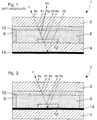
- FIG. 2 is a sectional view of a display device 1 according to a first embodiment of the present invention.
- a such display device 1 consists of a front substrate 2 arranged on the side where the light penetrates, and a rear substrate 4 which extends opposite the front substrate 2 and parallel to the latter.
- the two front 2 and rear 4 substrates are connected by a sealing frame 6 which delimits between them a cavity for the confinement of a film or layer 8 of reflective liquid crystal.
- the surface of the front substrate 2 facing the rear substrate 4 carries a first group of electrodes 10, and the surface of the substrate rear 4 facing the front substrate 2 carries a second group of electrodes 12.
- the black absorbent layer 14 is no longer located on the underside of the rear substrate 4, but at a more higher than the latter in the stacking order of substrates 2 and 4, considering as the lowest level, the underside of the rear substrate 4 facing the face of this same substrate 4 which carries the second group of electrodes 12. More precisely, the black absorbent layer 14 is disposed between the rear substrate 4 and the second group of electrodes 12.
- the black absorbent layer 14 is deposited on the second group of electrodes 12.
- This second alternative embodiment of the display device 1 according to the invention eliminates the reflections R3 and R4 and is therefore even more favorable from the standpoint of CR display contrast as the embodiment shown in Figure 2. Indeed, the drop in reflectivity r of the display device 1 when the liquid crystal is in the transparent state is stronger, which implies a an even more significant increase in CR display contrast.
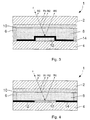
- Figure 4 is a sectional view in a display device 1 according to the invention in which the second group of electrodes 12 carried by the rear substrate 4 is made of an electrically conductive material of black color and is associated to an absorbent and insulating layer 14 also of black color which covers at minus the parts of the rear substrate not covered by the electrodes 12.
- the absorbent layer black 14 covers only the areas of the rear substrate 4 not covered by the electrodes 12.
- the black absorbent layer 14 is made of a material electrically non-conductive with a reflection coefficient close to or equal to that of the material used to prepare the black electrodes 12.
- this embodiment is as advantageous as that shown in Figure 3. It allows, in fact, to eliminate the reflections R3 and R4 which correspond, respectively, to the reflection of light incident at the interface between layer 8 of liquid crystal and the second group of electrodes 12, and on the reflection of the incident light at the interface between said second group of electrodes 12 and the front face of the rear substrate 4. Consequently, the reflectivity coefficient r decreases, which leads to an increase in contrast CR display.
- the mode of embodiment shown in Figure 4 has the advantage that we do not observe voltage drop due to the presence of the black layer 14 between the electrodes 12 and the layer of liquid crystal 8.
- This voltage drop indeed requires a voltage of higher control of electrodes 10 and 12, which obviously leads to increased power consumption, and requires that the black absorbent layer 14 has a thickness as constant as possible in order to maintain the control voltage at a uniform value for all the electrodes of the display device. So you have to use printing techniques that allow rigorous control of the thickness of the black absorbent layer 14, this which has the effect of increasing the manufacturing costs of the display device. Through against, in the case of the display device of FIG. 4, the thickness of the layer absorbent black 12 plays a less important role, which allows the use of simpler and therefore less expensive printing techniques.
- the amount of light R5 reflected by said electrodes 12 and by said absorbent layer 14 is identical. Therefore, in areas where the liquid crystal 8 is switched in the same transparent or reflecting state, the light will be absorbed almost identically by the black layer 14 and by the 12 black electrodes, and therefore provide a contrasting and very colorful display homogeneous over the entire surface of said display device 1. The electrodes will therefore not be able to detach visually from the rest of the display surface of the device according to the invention, so that these electrodes will be completely invisible for the observer.
- FIG. 5 is a sectional view of a display device 1 according to the invention in which the second group of electrodes 12 carried by the rear substrate 4 is produced in an electrically conductive material of black color and is covered by the black absorbent layer 14. From the point of view of optical losses, this mode of embodiment is as advantageous as that illustrated in FIG. 4 but is easier to achieve. Indeed, instead of the black absorbent layer 14 covering only the parts of the rear substrate 4 not covered by the black electrodes 12, it covers the entire surface of said rear substrate 4. The deposition of the layer absorbent black 14 is therefore greatly simplified and requires precision less, resulting in substantial time savings Manufacturing.
- FIG. 6 is a sectional view of a display device 1 according to the invention in which the black absorbent layer 14 is disposed between the rear substrate 4 and the second group of electrodes 12 made of an electrically conductive material black in color. From the point of view of optical losses as from the point of view of manufacturing, this embodiment is as advantageous as that illustrated in FIG. 5. Indeed, the black absorbent layer 14 covers the entire surface of the rear substrate 4 and can therefore be deposited without requiring special care. On the other hand, as the coefficient of reflection of the absorbent layer 14 is equal to or close to that of black electrodes 12, the amount of light reflected by said layer 14 and by said electrodes 12 will be substantially the same, so that a very homogeneous display over the entire surface of the display device 1.
- FIG 7 is a sectional view in a display device 1 according to the invention in which the black absorbent layer 14 is made in one piece with the rear substrate 4.
- the rear substrate 4 is made of glass or a plastic material dyed black in the mass.
- This embodiment of the device display 1 according to the invention is also advantageous, from the point of view of the yield optical, as the embodiments illustrated in Figures 5 and 6. It presents however, an additional advantage insofar as the rear substrate 4 playing both the role of electrode support and that of black absorbent layer, the step of depositing said absorbent layer is eliminated, which makes it possible to carry out saving manufacturing time and therefore reducing the cost price of the device display 1.
- the present invention relates (see FIG. 8) to a liquid crystal display device 1 comprising a transparent substrate 16 arranged on a front side, that is to say on the side receiving an incident light, and a layer 18 arranged on a rear side, so that this layer 18 extends in look of the substrate 16 parallel to the latter.
- Layer 18 plays the role held by the rear substrate 4 described above.
- the front substrate 16 and the layer 18 carry on their facing faces a first group of transparent electrodes 20 and a second group of electrodes 22 respectively.
- the electrodes 20 and 22 can be arranged, for example, in the form of strips perpendicular to each other.
- a film 24 formed by a plurality of liquid crystal capsules or by a liquid crystal dispersed in a polymer is placed between the front substrate 16 and the layer 18.
- the layer 18 is a black absorbent layer made of an electrically non-material conductive, while the second group of electrodes 22 is made of a material electrically conductive also black.
- the reflection coefficient of the material used to develop the black absorbent layer 18 is close to or equal to that of the material used to structure the electrodes 22.
- the rear substrate 4 which is conventionally made of a rigid material such as glass or a semi-rigid material such as plastic, and replace it with the black absorbent layer 26 which can be filed by all kinds of methods such as printing, evaporation or the like directly on the black electrodes 22. productivity gains which have a favorable impact on the cost price of the finished product.
- the electrically conductive material of color black used to make the second group of electrodes can be, as desired, an adhesive or a black varnish charged with conductive particles such as particles of carbon.
- conductive particles such as particles of carbon.
- this may include a resin and a hardener, one of these two components being charged with the particles conductive. It is advantageous to use the product sold under the name Carbon Light Lack SD 2841 by Lack Verke GmbH.
- This absorbent layer can be made, for example, in a colored insulating lacquer black such as that marketed under the name Heatsinkpaste HSP 2741 by the Lack Verke GmbH.
- the present invention sets out works with intrinsically reflective liquid crystals, that is to say reflecting the light without using reflectors in a first switching state, and being substantially transparent to light in a second switching state.
- these liquid crystals mention may of course be made of textured liquid crystals cholesteric, but also the liquid crystal / polymer structures formed by holography or some liquid crystals dispersed in a polymer, better known by their Anglo-Saxon name “Polymer Dispersed Liquid Crystal” or "PDLC”.
Landscapes
- Physics & Mathematics (AREA)
- Nonlinear Science (AREA)
- Chemical & Material Sciences (AREA)
- Crystallography & Structural Chemistry (AREA)
- General Physics & Mathematics (AREA)
- Optics & Photonics (AREA)
- Mathematical Physics (AREA)
- Dispersion Chemistry (AREA)
- Liquid Crystal (AREA)
Priority Applications (1)
| Application Number | Priority Date | Filing Date | Title |
|---|---|---|---|
| EP00204224A EP1209512A1 (de) | 2000-11-27 | 2000-11-27 | Reflektierende Flüssigkristallanzeige mit verbessertem Kontrast |
Applications Claiming Priority (1)
| Application Number | Priority Date | Filing Date | Title |
|---|---|---|---|
| EP00204224A EP1209512A1 (de) | 2000-11-27 | 2000-11-27 | Reflektierende Flüssigkristallanzeige mit verbessertem Kontrast |
Publications (1)
| Publication Number | Publication Date |
|---|---|
| EP1209512A1 true EP1209512A1 (de) | 2002-05-29 |
Family
ID=8172345
Family Applications (1)
| Application Number | Title | Priority Date | Filing Date |
|---|---|---|---|
| EP00204224A Withdrawn EP1209512A1 (de) | 2000-11-27 | 2000-11-27 | Reflektierende Flüssigkristallanzeige mit verbessertem Kontrast |
Country Status (1)
| Country | Link |
|---|---|
| EP (1) | EP1209512A1 (de) |
Cited By (3)
| Publication number | Priority date | Publication date | Assignee | Title |
|---|---|---|---|---|
| EP1225471A3 (de) * | 2001-01-17 | 2004-03-03 | Eastman Kodak Company | Anzeigefläche mit elektrisch leitender Verbundschicht und Polymerdispergierter Flüssigkristallschicht |
| EP1647858A1 (de) * | 2004-10-18 | 2006-04-19 | Ecsibeo Ab | Cholseterisches Flüssigkristallanzeigesystem und Verfahren zur Herstellung |
| EP2009468B1 (de) * | 2007-06-29 | 2011-10-19 | Varioptic | Elektrobenetzungsvorrichtung mit Polymerelektrode |
Citations (6)
| Publication number | Priority date | Publication date | Assignee | Title |
|---|---|---|---|---|
| US3734597A (en) * | 1968-02-23 | 1973-05-22 | Ncr Co | Process for producing a color state in a display device |
| JPS6240430A (ja) * | 1985-08-19 | 1987-02-21 | Seiko Epson Corp | 液晶ライトバルブ |
| JPH05150227A (ja) * | 1991-11-29 | 1993-06-18 | Kyocera Corp | 液晶表示装置 |
| WO1995007494A1 (en) * | 1993-09-08 | 1995-03-16 | Philips Electronics N.V. | Display device comprising an electro-optical medium |
| US6005651A (en) * | 1992-08-04 | 1999-12-21 | Matsushita Electric Industrial Co., Ltd. | Display panel and projection display system with use of display panel |
| US6124908A (en) * | 1996-06-10 | 2000-09-26 | Minolta Co., Ltd. | Liquid crystal element |
-
2000
- 2000-11-27 EP EP00204224A patent/EP1209512A1/de not_active Withdrawn
Patent Citations (6)
| Publication number | Priority date | Publication date | Assignee | Title |
|---|---|---|---|---|
| US3734597A (en) * | 1968-02-23 | 1973-05-22 | Ncr Co | Process for producing a color state in a display device |
| JPS6240430A (ja) * | 1985-08-19 | 1987-02-21 | Seiko Epson Corp | 液晶ライトバルブ |
| JPH05150227A (ja) * | 1991-11-29 | 1993-06-18 | Kyocera Corp | 液晶表示装置 |
| US6005651A (en) * | 1992-08-04 | 1999-12-21 | Matsushita Electric Industrial Co., Ltd. | Display panel and projection display system with use of display panel |
| WO1995007494A1 (en) * | 1993-09-08 | 1995-03-16 | Philips Electronics N.V. | Display device comprising an electro-optical medium |
| US6124908A (en) * | 1996-06-10 | 2000-09-26 | Minolta Co., Ltd. | Liquid crystal element |
Non-Patent Citations (2)
| Title |
|---|
| PATENT ABSTRACTS OF JAPAN vol. 011, no. 223 (P - 597) 21 July 1987 (1987-07-21) * |
| PATENT ABSTRACTS OF JAPAN vol. 017, no. 539 (P - 1621) 28 September 1993 (1993-09-28) * |
Cited By (6)
| Publication number | Priority date | Publication date | Assignee | Title |
|---|---|---|---|---|
| EP1225471A3 (de) * | 2001-01-17 | 2004-03-03 | Eastman Kodak Company | Anzeigefläche mit elektrisch leitender Verbundschicht und Polymerdispergierter Flüssigkristallschicht |
| EP1647858A1 (de) * | 2004-10-18 | 2006-04-19 | Ecsibeo Ab | Cholseterisches Flüssigkristallanzeigesystem und Verfahren zur Herstellung |
| WO2006042737A1 (en) * | 2004-10-18 | 2006-04-27 | Ecsibeo Ab | Cholesteric liquid crystal display (lcd) device, and method for its production |
| CN100480828C (zh) * | 2004-10-18 | 2009-04-22 | 拉谢扎·科米托弗 | 胆甾相液晶显示(lcd)器件及其制造方法 |
| US7916255B2 (en) | 2004-10-18 | 2011-03-29 | Lachezar Komitov | Cholesteric liquid crystal display (LCD) device, and method for its production |
| EP2009468B1 (de) * | 2007-06-29 | 2011-10-19 | Varioptic | Elektrobenetzungsvorrichtung mit Polymerelektrode |
Similar Documents
| Publication | Publication Date | Title |
|---|---|---|
| EP0872759B1 (de) | Flüssigkristallanzeige-Vorrichtung für einen farbigen Bildschirm | |
| EP1040391B1 (de) | Anzeigeeinheit mit zwei übereinander liegenden anzeigevorrichtungen | |
| EP2963506B1 (de) | Anzeigeeinheit, die zwei übereinandergelagerte anzeigevorrichtungen umfasst | |
| US6753937B2 (en) | Reflective liquid crystal display device having a black absorbent layer | |
| EP3006994B1 (de) | Anzeigeeinheit, die zwei übereinandergelagerte Anzeigevorrichtungen umfasst | |
| EP0786685B1 (de) | Verzierung anzeigende Vorrichtung und diese enthaltende Uhr | |
| EP3650958B1 (de) | Gegenstand, der mit einer elektrooptischen anzeigevorrichtung ausgestattet ist | |
| FR2765697A1 (fr) | Procede de production de deux domaines au sein d'une couche de cristal liquide | |
| CH647337A5 (fr) | Dispositif electro-optique a cristaux liquides chiraux smectiques c ou h. | |
| FR2907559A1 (fr) | Composant optique elecro-commandable comprenant un ensemble de cellules | |
| EP3650957B1 (de) | Gegenstand, der mit einer elektrooptischen anzeigevorrichtung ausgestattet ist | |
| EP0235634B1 (de) | Anzeigezelle | |
| FR2939916A1 (fr) | Element optique a puissance variable | |
| EP3007015A1 (de) | Hybridanzeigeeinheit, die eine solarzelle umfasst | |
| EP1074863B1 (de) | Optischer Bragg-Reflektor und Verfahren zu dessen Herstellung | |
| FR2489993A1 (fr) | Dispositif d'affichage a cristaux liquides avec fonction anti-reflechissante | |
| WO2012175250A1 (fr) | Afficheur a cristal liquide a electrodes d'effacement | |
| EP1209512A1 (de) | Reflektierende Flüssigkristallanzeige mit verbessertem Kontrast | |
| EP1518145A2 (de) | Anzeigezelle, insbesondere flüssigkristall- oder photovoltaische zelle mit mitteln zur verbindung mit einer elektronischen steuerschaltung | |
| EP2963505A1 (de) | Anzeigeeinheit, die zwei sich überlagernde Anzeigevorrichtungen umfasst | |
| FR2877737A1 (fr) | Afficheur ophtalmique comportant une lentille ophtalmique et un imageur optique | |
| EP1202109A1 (de) | Flüssigkristallanzeigeeinrichtung mit hohem Reflexionskoeffizienten | |
| EP1324110B1 (de) | Flüssigkristallzelle mit mindestens zwei Beugungsgittern insbesondere für einen optischen Strahlteiler | |
| CH715286B1 (fr) | Objet muni d'un dispositif d`affichage électrooptique. | |
| CH620774A5 (de) |
Legal Events
| Date | Code | Title | Description |
|---|---|---|---|
| PUAI | Public reference made under article 153(3) epc to a published international application that has entered the european phase |
Free format text: ORIGINAL CODE: 0009012 |
|
| AK | Designated contracting states |
Kind code of ref document: A1 Designated state(s): AT BE CH CY DE DK ES FI FR GB GR IE IT LI LU MC NL PT SE TR |
|
| AX | Request for extension of the european patent |
Free format text: AL;LT;LV;MK;RO;SI |
|
| 17P | Request for examination filed |
Effective date: 20021129 |
|
| AKX | Designation fees paid |
Designated state(s): CH DE FR GB IT LI |
|
| 17Q | First examination report despatched |
Effective date: 20041203 |
|
| GRAP | Despatch of communication of intention to grant a patent |
Free format text: ORIGINAL CODE: EPIDOSNIGR1 |
|
| STAA | Information on the status of an ep patent application or granted ep patent |
Free format text: STATUS: THE APPLICATION IS DEEMED TO BE WITHDRAWN |
|
| 18D | Application deemed to be withdrawn |
Effective date: 20060719 |