EP1209522A2 - Maske zur herstellung von Bildschirmen - Google Patents
Maske zur herstellung von Bildschirmen Download PDFInfo
- Publication number
- EP1209522A2 EP1209522A2 EP01128145A EP01128145A EP1209522A2 EP 1209522 A2 EP1209522 A2 EP 1209522A2 EP 01128145 A EP01128145 A EP 01128145A EP 01128145 A EP01128145 A EP 01128145A EP 1209522 A2 EP1209522 A2 EP 1209522A2
- Authority
- EP
- European Patent Office
- Prior art keywords
- mask
- sub
- frame
- main frame
- masks
- Prior art date
- Legal status (The legal status is an assumption and is not a legal conclusion. Google has not performed a legal analysis and makes no representation as to the accuracy of the status listed.)
- Granted
Links
Images


Classifications
-
- C—CHEMISTRY; METALLURGY
- C23—COATING METALLIC MATERIAL; COATING MATERIAL WITH METALLIC MATERIAL; CHEMICAL SURFACE TREATMENT; DIFFUSION TREATMENT OF METALLIC MATERIAL; COATING BY VACUUM EVAPORATION, BY SPUTTERING, BY ION IMPLANTATION OR BY CHEMICAL VAPOUR DEPOSITION, IN GENERAL; INHIBITING CORROSION OF METALLIC MATERIAL OR INCRUSTATION IN GENERAL
- C23C—COATING METALLIC MATERIAL; COATING MATERIAL WITH METALLIC MATERIAL; SURFACE TREATMENT OF METALLIC MATERIAL BY DIFFUSION INTO THE SURFACE, BY CHEMICAL CONVERSION OR SUBSTITUTION; COATING BY VACUUM EVAPORATION, BY SPUTTERING, BY ION IMPLANTATION OR BY CHEMICAL VAPOUR DEPOSITION, IN GENERAL
- C23C14/00—Coating by vacuum evaporation, by sputtering or by ion implantation of the coating forming material
- C23C14/04—Coating on selected surface areas, e.g. using masks
- C23C14/042—Coating on selected surface areas, e.g. using masks using masks
-
- H—ELECTRICITY
- H05—ELECTRIC TECHNIQUES NOT OTHERWISE PROVIDED FOR
- H05B—ELECTRIC HEATING; ELECTRIC LIGHT SOURCES NOT OTHERWISE PROVIDED FOR; CIRCUIT ARRANGEMENTS FOR ELECTRIC LIGHT SOURCES, IN GENERAL
- H05B33/00—Electroluminescent light sources
- H05B33/10—Apparatus or processes specially adapted to the manufacture of electroluminescent light sources
-
- H—ELECTRICITY
- H10—SEMICONDUCTOR DEVICES; ELECTRIC SOLID-STATE DEVICES NOT OTHERWISE PROVIDED FOR
- H10K—ORGANIC ELECTRIC SOLID-STATE DEVICES
- H10K71/00—Manufacture or treatment specially adapted for the organic devices covered by this subclass
-
- H—ELECTRICITY
- H10—SEMICONDUCTOR DEVICES; ELECTRIC SOLID-STATE DEVICES NOT OTHERWISE PROVIDED FOR
- H10K—ORGANIC ELECTRIC SOLID-STATE DEVICES
- H10K71/00—Manufacture or treatment specially adapted for the organic devices covered by this subclass
- H10K71/10—Deposition of organic active material
- H10K71/16—Deposition of organic active material using physical vapour deposition [PVD], e.g. vacuum deposition or sputtering
- H10K71/166—Deposition of organic active material using physical vapour deposition [PVD], e.g. vacuum deposition or sputtering using selective deposition, e.g. using a mask
Definitions
- the present invention relates to a mask for fabricating a large sized display panel.
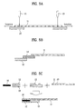
- a shadow mask of a strip type as shown in FIG. 1A, or a delta type as shown in FIG. 1B is required for deposition of luminescent material layers of R, G, B pixels invariably.
- those masks are liable to sag due to patterns on the masks, to damage barriers and the like formed on the panel during deposition of the material, particularly, the strip type shadow mask in which rectangular elongated patterns are formed has a greater sag than the delta type shadow mask.
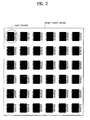
- the sagging of the shadow mask becomes more greater when unit devices are mass produced on a large sized substrate, because, as shown in FIG. 3, the size of the shadow mask is required to be large the same as the substrate, and many patterns are formed on the shadow mask.
- metal stripes on the mask are susceptible to vibration even by a weak impact, to give damage to the barriers of the panel. That is, since a gap between the shadow mask and the panel is very small, the vibration to the mask gives damage to the barriers at the highest positions among the barriers formed on the panel, which may cause shorts between pixels in fabrication of second electrodes.
- the present invention is directed to a mask for fabricating a display panel that substantially obviates one or more of the problems due to limitations and disadvantages of the related art.
- An object of the present invention is to provide a mask for fabricating a display panel, which has no sagging, or shadowing.
- Another object of the present invention is to provide a mask for fabricating a display panel, which is suitable for fabrication of a large sized, or mass production of, display panel.
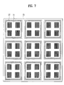
- the present invention suggests to fabricate a main frame having a plurality of holes, and fitting sub-masks in the holes respectively according to panel sizes and patterns intended to fabricate, for providing a mask suitable for fabrication of large sized, or mass production of, display panels that have neither sagging, nor shadowing.
- FIG. 4 illustrates a sub-mask in accordance with a preferred embodiment of the present invention.
- the sub-mask in accordance with a preferred embodiment of the present invention includes a sub-mask 11 having at least one pattern, and a sub-frame 12 fixed to edges around the sub-mask 11 for fastening the sub-frame.
- the sub-mask 11 may have a pattern formed thereon varied as a designer desires, or a plurality of patterns, within a limit the patterns cause no sagging of the sub-mask 11.
- the sub-frame 12 fixed around the sub-mask 11 may be formed of metal, polymer, inorganic material, or the like, which is formable, and strong against bending, such as aluminum, nickel, tungsten, titanium, iron, copper, or an alloy of them in metal, or plastic in polymer, or glass, or wafer in inorganic material.
- the sub-mask 11 is mounted on the sub-frame 12, tension is applied to the sub-mask 11 uniformly for preventing sagging of the sub-mask 11, and the sub-mask 11 is fixed to the sub-frame 12 by using a laser 13.
- a piece of fiber 14 like a net is attached around the sub-mask 11 with adhesive, and tension is applied to the fiber 14 for fixing to the sub-frame 12.
- the fiber 14 is attached to the sub-mask 11 and the sub-frame 12 with adhesive.
- a jig 15 may be used. That is, holes 17 are formed in edge region of the sub-mask 11, lateral holes 18 passed through sides of the sub-frame 12 are formed, the sub-mask 11 is fastened to the jig 15 by using the holes 17, and the sub-frame 12 is fastened to the jig 15 with screws 16, to fix the sub-mask 11 to the sub-frame 12.
- the sub-mask fabricated thus is mounted on the main frame 21, a mask for fabricating a large display panel can be fabricated.
- the sub-mask 11 is fitted to every hole in the main frame 21.
- a number of holes in the main frame 21 are dependent on a number of devices to be fabricated, and the number of holes in the main frame 21 is required to be more than the number of the sub-mask 11 to be mounted on the main frame 21, because there may be a case when the sub-masks 11 are mounted only in holes at required positions according to forms of devices a designer intends to fabricate.
- the main frame 21 is fabricated to have a size equal to, or greater than a panel size a material is to be deposited thereon.
- the sub-mask 11 is fabricated to be movable in the hole in the main frame 21 in up and down, and left and right directions, for fine adjustment of the sub-mask 11 to align the patterns on the sub-mask 11 at an exact positions, by using MEMS (Microelectric Machine System).
- MEMS Microelectric Machine System
- the main frame 21 may be formed of metal, polymer, or inorganic material, or the like, which are formable and strong against bending, such as aluminum, tungsten, titanium, iron, copper, or an alloy of them as the metal, plastic as the polymer, or glass or wafer as the inorganic material.
- a large sized transparent substrate is provided, first electrode stripes, first electrode pads, and second electrode pads are formed on the substrate, and barriers are formed between luminescent regions perpendicular to the first electrodes.
- a large sized mask of the present invention is placed on the substrate, and fine adjustment of positions of the sub-masks is made for accurate alignment of the patterns on the sub-mask with the luminescent regions on the substrate.
- a red luminescent layer is deposited on a red luminescent region of the substrate, and the large sized mask is moved.
- a green luminescent layer is deposited on a green luminescent region of the substrate, and the large sized mask is moved, again.
- a blue luminescent layer is deposited on a blue luminescent region of the substrate.
- a second electrode material is deposited on an entire surface of the substrate, to form the second electrode stripes in the luminescent region.
- a protection film is formed on the second electrode, encapsulation is conducted, to complete fabrication of the organic EL display panel.
- the mask for fabricating a display panel of the present invention is not involved in sagging, or shadowing, the mask of the present invention can improve a fabrication accuracy, and reliability, and is suitable for fabrication of large sized panel, or mass production, thereby dropping a fabrication cost. Moreover, the possibility of mounting/dismounting of mask makes maintenance of the mask easy.
Landscapes
- Chemical & Material Sciences (AREA)
- Engineering & Computer Science (AREA)
- Chemical Kinetics & Catalysis (AREA)
- Materials Engineering (AREA)
- Mechanical Engineering (AREA)
- Metallurgy (AREA)
- Organic Chemistry (AREA)
- Manufacturing & Machinery (AREA)
- Electroluminescent Light Sources (AREA)
- Physical Vapour Deposition (AREA)
- Devices For Indicating Variable Information By Combining Individual Elements (AREA)
- Gas-Filled Discharge Tubes (AREA)
Applications Claiming Priority (2)
| Application Number | Priority Date | Filing Date | Title |
|---|---|---|---|
| KR10-2000-0071327A KR100382491B1 (ko) | 2000-11-28 | 2000-11-28 | 유기 el의 새도우 마스크 |
| KR2000071327 | 2000-11-28 |
Publications (3)
| Publication Number | Publication Date |
|---|---|
| EP1209522A2 true EP1209522A2 (de) | 2002-05-29 |
| EP1209522A3 EP1209522A3 (de) | 2004-09-29 |
| EP1209522B1 EP1209522B1 (de) | 2010-06-16 |
Family
ID=19702008
Family Applications (1)
| Application Number | Title | Priority Date | Filing Date |
|---|---|---|---|
| EP01128145A Expired - Lifetime EP1209522B1 (de) | 2000-11-28 | 2001-11-27 | Maske zur Herstellung von Bildschirmen |
Country Status (6)
| Country | Link |
|---|---|
| US (1) | US6866720B2 (de) |
| EP (1) | EP1209522B1 (de) |
| JP (1) | JP2002221912A (de) |
| KR (1) | KR100382491B1 (de) |
| CN (1) | CN1209681C (de) |
| DE (1) | DE60142385D1 (de) |
Cited By (16)
| Publication number | Priority date | Publication date | Assignee | Title |
|---|---|---|---|---|
| GB2382820A (en) * | 2001-12-05 | 2003-06-11 | Samsung Nec Mobile Display Co | Tension mask assembly for use in vacuum deposition of thin film of an organic electroluminescent device |
| WO2004061149A1 (en) * | 2002-12-31 | 2004-07-22 | Eastman Kodak Company | Flexible frame for mounting a deposition mask |
| EP1391783A3 (de) * | 2002-08-01 | 2004-08-04 | Eastman Kodak Company | Methode und Geräte zur Herstellung einer Matrix von Belichtungsmasken |
| EP1584703A1 (de) * | 2004-03-23 | 2005-10-12 | Seiko Epson Corporation | Mask, Verfahren zu seiner Herstellung, Verfahren zur Herstellung eines Dünnschichtmusters, Verfahren zur Herstellung einer elektro-optischen Vorrichtung und elektronisches Apparat |
| EP1626103A2 (de) | 2004-07-15 | 2006-02-15 | Samsung SDI Co., Ltd. | Lochmasken-Rahmenanordnung für die Abscheidung von dünnen Schichten und mittels dieser Anordnung hergestellte organische lichtemittierende Anzeigevorrichtung |
| EP1378933A3 (de) * | 2002-07-03 | 2006-04-19 | Lg Electronics Inc. | Schattenmaske für die Herstellung eines flachen Displays |
| EP1437926A4 (de) * | 2001-08-24 | 2007-07-04 | Dainippon Printing Co Ltd | Maskeneinrichtung zur bildung mehrerer seiten für die vakuumablagerung |
| WO2007099518A1 (en) * | 2006-03-03 | 2007-09-07 | Ecole Polytechnique Federale De Lausanne (Epfl) | Stencil mask for accurate pattern replication |
| CN100354752C (zh) * | 2002-05-31 | 2007-12-12 | 三星Sdi株式会社 | 用于蒸发的掩模,包括该掩模的掩模框架组件,及其制造方法 |
| CN100464440C (zh) * | 2002-06-03 | 2009-02-25 | 三星移动显示器株式会社 | 用于有机电致发光装置的薄层真空蒸发的掩模框组件 |
| EP2063320A3 (de) * | 2007-11-20 | 2009-07-29 | Samsung Mobile Display Co., Ltd. | Verfahren und Vorrichtung zur Herstellung einer vertikalen Beschichtungsmaske |
| CN101280411B (zh) * | 2007-04-05 | 2011-06-29 | 三星移动显示器株式会社 | 用于平板显示器薄膜沉积的掩模框架组件和使用该组件的沉积设备 |
| US20120145076A1 (en) * | 2010-12-14 | 2012-06-14 | Samsung Mobile Display Co., Ltd. | Mask frame assembly for thin film deposition and the manufacturing method thereof |
| JP2015145532A (ja) * | 2014-01-23 | 2015-08-13 | 上海和輝光電有限公司Everdisplay Optronics (Shanghai) Limited | マスク装置、該マスク装置を製造するためのシステム及び方法 |
| WO2017117999A1 (zh) * | 2016-01-06 | 2017-07-13 | 京东方科技集团股份有限公司 | 金属掩模板及其制作方法 |
| CN110767689A (zh) * | 2018-10-31 | 2020-02-07 | 云谷(固安)科技有限公司 | 掩膜板、显示面板、其制备方法及显示终端 |
Families Citing this family (40)
| Publication number | Priority date | Publication date | Assignee | Title |
|---|---|---|---|---|
| KR100472012B1 (ko) * | 2001-12-17 | 2005-03-08 | 조수제 | 섀도우 마스크 및 그 제조 방법 |
| US6821348B2 (en) * | 2002-02-14 | 2004-11-23 | 3M Innovative Properties Company | In-line deposition processes for circuit fabrication |
| US6897164B2 (en) * | 2002-02-14 | 2005-05-24 | 3M Innovative Properties Company | Aperture masks for circuit fabrication |
| US20030151118A1 (en) * | 2002-02-14 | 2003-08-14 | 3M Innovative Properties Company | Aperture masks for circuit fabrication |
| US6727125B2 (en) * | 2002-04-17 | 2004-04-27 | Sharp Laboratories Of America, Inc. | Multi-pattern shadow mask system and method for laser annealing |
| US20030221620A1 (en) * | 2002-06-03 | 2003-12-04 | Semiconductor Energy Laboratory Co., Ltd. | Vapor deposition device |
| KR100499476B1 (ko) * | 2002-07-22 | 2005-07-05 | 엘지전자 주식회사 | 유기 el 소자의 새도우 마스크 |
| KR100698044B1 (ko) * | 2002-10-19 | 2007-03-23 | 엘지.필립스 엘시디 주식회사 | 마스크 설계 방법 및 패널 형성 방법 |
| KR100463532B1 (ko) * | 2002-10-22 | 2004-12-29 | 엘지전자 주식회사 | 대면적 풀-컬러 디스플레이 패널의 제작방법 |
| JP4089632B2 (ja) * | 2003-03-07 | 2008-05-28 | セイコーエプソン株式会社 | マスクの製造方法、マスクの製造装置、発光材料の成膜方法 |
| KR100534580B1 (ko) * | 2003-03-27 | 2005-12-07 | 삼성에스디아이 주식회사 | 표시장치용 증착 마스크 및 그의 제조방법 |
| KR100676177B1 (ko) * | 2005-03-22 | 2007-02-01 | 엘지전자 주식회사 | 유기전계발광표시소자의 제조장치 |
| KR100662558B1 (ko) * | 2005-12-13 | 2006-12-28 | 삼성전자주식회사 | 마스크 및 이를 이용한 디스플레이장치의 제조방법 |
| KR100775846B1 (ko) * | 2006-09-04 | 2007-11-13 | 엘지전자 주식회사 | 디스플레이 소자 제조용 마스크 |
| TWI398533B (zh) * | 2009-12-29 | 2013-06-11 | Au Optronics Corp | 蔭罩及其製作方法 |
| KR101182440B1 (ko) * | 2010-01-11 | 2012-09-12 | 삼성디스플레이 주식회사 | 박막 증착용 마스크 프레임 조립체 |
| CN102110787B (zh) * | 2010-11-05 | 2012-07-25 | 四川虹视显示技术有限公司 | Oled掩膜板对位方法 |
| KR101693578B1 (ko) * | 2011-03-24 | 2017-01-10 | 삼성디스플레이 주식회사 | 증착 마스크 |
| JP5890252B2 (ja) * | 2012-05-30 | 2016-03-22 | 日本航空電子工業株式会社 | 電気コネクタ |
| US9583363B2 (en) | 2012-12-31 | 2017-02-28 | Sunedison Semiconductor Limited (Uen201334164H) | Processes and apparatus for preparing heterostructures with reduced strain by radial distension |
| KR20140109699A (ko) * | 2013-03-06 | 2014-09-16 | 삼성디스플레이 주식회사 | 마스크 구조체와 이를 포함하는 마스크 조립체 및 마스크 구조체 제조방법 |
| KR20140125191A (ko) * | 2013-04-18 | 2014-10-28 | 삼성디스플레이 주식회사 | 증착 장치 |
| CN103235451A (zh) * | 2013-04-23 | 2013-08-07 | 北京京东方光电科技有限公司 | 掩膜板及其制造方法 |
| GB201311738D0 (en) * | 2013-06-29 | 2013-08-14 | British Telecomm | Apparatus |
| KR20170084088A (ko) * | 2014-10-17 | 2017-07-19 | 어드밴텍 글로벌, 리미티드 | 다중 마스크 정렬 시스템 및 방법 |
| US10745796B2 (en) * | 2014-10-17 | 2020-08-18 | Advantech Global, Ltd | Multi-mask alignment system and method |
| CN105986225A (zh) * | 2015-02-16 | 2016-10-05 | 上海和辉光电有限公司 | Oled蒸镀用的屏蔽层及其制作方法 |
| KR102404575B1 (ko) * | 2015-10-12 | 2022-06-03 | 삼성디스플레이 주식회사 | 증착 장치와 이를 이용한 유기 발광 디스플레이 장치의 제조 방법 |
| CN106527041B (zh) | 2016-10-10 | 2018-10-09 | 南京中电熊猫液晶显示科技有限公司 | 掩膜版及其曝光方法、以及液晶显示面板 |
| JP7487481B2 (ja) | 2019-02-06 | 2024-05-21 | 大日本印刷株式会社 | 蒸着マスク装置、マスク支持機構及び蒸着マスク装置の製造方法 |
| CN109750257B (zh) * | 2019-03-26 | 2021-03-26 | 京东方科技集团股份有限公司 | 掩膜板及其制造方法 |
| KR101999360B1 (ko) * | 2019-05-14 | 2019-07-11 | 주식회사 핌스 | 박막 증착용 마스크 조립체를 위한 복합 프레임 요소 및 그 제조 방법 |
| CN111020477B (zh) * | 2019-11-29 | 2021-12-21 | 武汉天马微电子有限公司 | 一种掩膜装置、蒸镀方法及显示面板 |
| KR20210091382A (ko) * | 2020-01-13 | 2021-07-22 | 삼성디스플레이 주식회사 | 마스크, 이의 제조 방법, 및 표시 패널 제조 방법 |
| KR102929156B1 (ko) | 2020-08-31 | 2026-02-24 | 삼성디스플레이 주식회사 | 마스크, 이의 제조 방법, 및 표시 패널 제조 방법 |
| KR20220034993A (ko) * | 2020-09-11 | 2022-03-21 | 삼성디스플레이 주식회사 | 증착 장치 및 증착 장치의 마스크 착좌 방법 |
| KR102435235B1 (ko) * | 2020-10-07 | 2022-08-24 | 주식회사 효산 | 마스크의 제조 방법 및 마스크 |
| US11659759B2 (en) * | 2021-01-06 | 2023-05-23 | Applied Materials, Inc. | Method of making high resolution OLED fabricated with overlapped masks |
| KR20230056129A (ko) * | 2021-10-19 | 2023-04-27 | 삼성디스플레이 주식회사 | 마스크, 이를 포함하는 마스크 어셈블리 및 마스크 제조 방법 |
| CN115747714A (zh) * | 2022-11-24 | 2023-03-07 | 黄石全洋光电科技有限公司 | 一种具有分离式网框的张网机及其张网加工方法 |
Citations (3)
| Publication number | Priority date | Publication date | Assignee | Title |
|---|---|---|---|---|
| US3352282A (en) | 1965-07-23 | 1967-11-14 | Bendix Corp | Vacuum deposit device including means to register and manipulate mask and substrate elements |
| JPH09120592A (ja) | 1995-10-23 | 1997-05-06 | Dainippon Printing Co Ltd | 成膜装置用マスク及びそれを利用する成膜基板 |
| DE29707686U1 (de) | 1997-04-28 | 1997-06-26 | Balzers Prozess Systeme Vertriebs- und Service GmbH, 81245 München | Magnethalterung für Folienmasken |
Family Cites Families (12)
| Publication number | Priority date | Publication date | Assignee | Title |
|---|---|---|---|---|
| JPS60181264A (ja) * | 1984-02-24 | 1985-09-14 | Konishiroku Photo Ind Co Ltd | 製膜方法およびその装置 |
| JP2815004B2 (ja) * | 1996-10-30 | 1998-10-27 | 日本電気株式会社 | 表示装置およびその製造方法 |
| JP4016220B2 (ja) * | 1997-06-10 | 2007-12-05 | ホーチキ株式会社 | 蒸着膜形成方法及び真空蒸着装置 |
| JP4058149B2 (ja) * | 1997-12-01 | 2008-03-05 | キヤノンアネルバ株式会社 | 真空成膜装置のマスク位置合わせ方法 |
| JP2848384B1 (ja) * | 1997-12-05 | 1999-01-20 | 日本電気株式会社 | 有機el表示装置及びその製造方法 |
| KR100282392B1 (ko) * | 1998-06-12 | 2001-02-15 | 구자홍 | 풀-컬러유기전계발광소자및그제조방법 |
| JP4282798B2 (ja) * | 1998-11-02 | 2009-06-24 | ローム株式会社 | Elディスプレイパネルおよびその製造方法 |
| US6146489A (en) * | 1998-11-19 | 2000-11-14 | General Electric Company | Method and apparatus for depositing scintillator material on radiation imager |
| JP3575303B2 (ja) * | 1998-11-26 | 2004-10-13 | トヨタ自動車株式会社 | 薄膜形成方法 |
| KR100595170B1 (ko) * | 1999-03-17 | 2006-07-03 | 엘지전자 주식회사 | 풀-컬러 유기 el 디스플레이 패널 및 그 제조방법 |
| KR100606439B1 (ko) * | 1999-04-08 | 2006-07-31 | 엘지.필립스 엘시디 주식회사 | 전기발광소자 제조방법 |
| JP2001237073A (ja) * | 2000-02-24 | 2001-08-31 | Tohoku Pioneer Corp | 多面取り用メタルマスク及びその製造方法 |
-
2000
- 2000-11-28 KR KR10-2000-0071327A patent/KR100382491B1/ko not_active Expired - Lifetime
-
2001
- 2001-11-27 DE DE60142385T patent/DE60142385D1/de not_active Expired - Lifetime
- 2001-11-27 US US09/993,521 patent/US6866720B2/en not_active Expired - Lifetime
- 2001-11-27 EP EP01128145A patent/EP1209522B1/de not_active Expired - Lifetime
- 2001-11-28 CN CNB011381612A patent/CN1209681C/zh not_active Expired - Lifetime
- 2001-11-28 JP JP2001362324A patent/JP2002221912A/ja active Pending
Patent Citations (3)
| Publication number | Priority date | Publication date | Assignee | Title |
|---|---|---|---|---|
| US3352282A (en) | 1965-07-23 | 1967-11-14 | Bendix Corp | Vacuum deposit device including means to register and manipulate mask and substrate elements |
| JPH09120592A (ja) | 1995-10-23 | 1997-05-06 | Dainippon Printing Co Ltd | 成膜装置用マスク及びそれを利用する成膜基板 |
| DE29707686U1 (de) | 1997-04-28 | 1997-06-26 | Balzers Prozess Systeme Vertriebs- und Service GmbH, 81245 München | Magnethalterung für Folienmasken |
Cited By (21)
| Publication number | Priority date | Publication date | Assignee | Title |
|---|---|---|---|---|
| EP1437926A4 (de) * | 2001-08-24 | 2007-07-04 | Dainippon Printing Co Ltd | Maskeneinrichtung zur bildung mehrerer seiten für die vakuumablagerung |
| US6858086B2 (en) | 2001-12-05 | 2005-02-22 | Samsung Oled Co., Ltd. | Tension mask assembly for use in vacuum deposition of thin film of organic electroluminescent device |
| GB2382820B (en) * | 2001-12-05 | 2005-04-20 | Samsung Nec Mobile Display Co | Tension mask assembly for use in vacuum deposition of thin film of organic electroluminescent device |
| GB2382820A (en) * | 2001-12-05 | 2003-06-11 | Samsung Nec Mobile Display Co | Tension mask assembly for use in vacuum deposition of thin film of an organic electroluminescent device |
| CN100354752C (zh) * | 2002-05-31 | 2007-12-12 | 三星Sdi株式会社 | 用于蒸发的掩模,包括该掩模的掩模框架组件,及其制造方法 |
| CN100464440C (zh) * | 2002-06-03 | 2009-02-25 | 三星移动显示器株式会社 | 用于有机电致发光装置的薄层真空蒸发的掩模框组件 |
| EP1378933A3 (de) * | 2002-07-03 | 2006-04-19 | Lg Electronics Inc. | Schattenmaske für die Herstellung eines flachen Displays |
| EP1391783A3 (de) * | 2002-08-01 | 2004-08-04 | Eastman Kodak Company | Methode und Geräte zur Herstellung einer Matrix von Belichtungsmasken |
| WO2004061149A1 (en) * | 2002-12-31 | 2004-07-22 | Eastman Kodak Company | Flexible frame for mounting a deposition mask |
| EP1584703A1 (de) * | 2004-03-23 | 2005-10-12 | Seiko Epson Corporation | Mask, Verfahren zu seiner Herstellung, Verfahren zur Herstellung eines Dünnschichtmusters, Verfahren zur Herstellung einer elektro-optischen Vorrichtung und elektronisches Apparat |
| EP1626103A2 (de) | 2004-07-15 | 2006-02-15 | Samsung SDI Co., Ltd. | Lochmasken-Rahmenanordnung für die Abscheidung von dünnen Schichten und mittels dieser Anordnung hergestellte organische lichtemittierende Anzeigevorrichtung |
| WO2007099518A1 (en) * | 2006-03-03 | 2007-09-07 | Ecole Polytechnique Federale De Lausanne (Epfl) | Stencil mask for accurate pattern replication |
| CN101280411B (zh) * | 2007-04-05 | 2011-06-29 | 三星移动显示器株式会社 | 用于平板显示器薄膜沉积的掩模框架组件和使用该组件的沉积设备 |
| EP2063320A3 (de) * | 2007-11-20 | 2009-07-29 | Samsung Mobile Display Co., Ltd. | Verfahren und Vorrichtung zur Herstellung einer vertikalen Beschichtungsmaske |
| US8459526B2 (en) | 2007-11-20 | 2013-06-11 | Samsung Display Co., Ltd. | Method and apparatus for fabricating vertical deposition mask |
| US20120145076A1 (en) * | 2010-12-14 | 2012-06-14 | Samsung Mobile Display Co., Ltd. | Mask frame assembly for thin film deposition and the manufacturing method thereof |
| US8869738B2 (en) * | 2010-12-14 | 2014-10-28 | Samsung Display Co., Ltd. | Mask frame assembly for thin film deposition and the manufacturing method thereof |
| JP2015145532A (ja) * | 2014-01-23 | 2015-08-13 | 上海和輝光電有限公司Everdisplay Optronics (Shanghai) Limited | マスク装置、該マスク装置を製造するためのシステム及び方法 |
| WO2017117999A1 (zh) * | 2016-01-06 | 2017-07-13 | 京东方科技集团股份有限公司 | 金属掩模板及其制作方法 |
| US10604833B2 (en) | 2016-01-06 | 2020-03-31 | Boe Technology Group Co., Ltd. | Metal mask plate and fabrication method thereof |
| CN110767689A (zh) * | 2018-10-31 | 2020-02-07 | 云谷(固安)科技有限公司 | 掩膜板、显示面板、其制备方法及显示终端 |
Also Published As
| Publication number | Publication date |
|---|---|
| US20020062785A1 (en) | 2002-05-30 |
| JP2002221912A (ja) | 2002-08-09 |
| KR20020041654A (ko) | 2002-06-03 |
| EP1209522B1 (de) | 2010-06-16 |
| US6866720B2 (en) | 2005-03-15 |
| CN1362642A (zh) | 2002-08-07 |
| DE60142385D1 (de) | 2010-07-29 |
| EP1209522A3 (de) | 2004-09-29 |
| KR100382491B1 (ko) | 2003-05-09 |
| CN1209681C (zh) | 2005-07-06 |
Similar Documents
| Publication | Publication Date | Title |
|---|---|---|
| US6866720B2 (en) | Mask for fabricating display panel | |
| US6858086B2 (en) | Tension mask assembly for use in vacuum deposition of thin film of organic electroluminescent device | |
| KR101070539B1 (ko) | 증착 마스크 및 이를 사용한 유기 전계 발광 장치의 제조 방법 | |
| CN109913809B (zh) | 一种掩膜装置及一种蒸镀方法 | |
| US7915073B2 (en) | Method of manufacturing the organic electroluminescent display and organic electroluminescent display manufactured by the method | |
| CN111088474B (zh) | 一种掩膜板及其制作方法 | |
| US20060110663A1 (en) | Mask for depositing thin film of flat panel display and method of fabricating the mask | |
| KR20170112673A (ko) | 증착용마스크 및 이를 이용한 oled 패널 | |
| CN109487206B (zh) | 掩膜版及采用该掩膜版的掩膜装置 | |
| JP4506214B2 (ja) | 有機電界発光装置およびその製造方法 | |
| TW201220490A (en) | capable of preventing the sag of the center of a frame by forming a rib in the center of the frame | |
| WO2020113751A1 (zh) | 一种掩膜板 | |
| KR102126515B1 (ko) | 마스크 조립체의 제조 장치 및 그 방법 | |
| CN103668048A (zh) | 一种复合掩模板组件的制作方法 | |
| JP7241048B2 (ja) | 基板支持装置および成膜装置 | |
| CN114981468B (zh) | 掩模板遮片和掩模板设备 | |
| JP2020532652A (ja) | 高分解能fmmのためのfmm処理 | |
| JP2006037203A (ja) | メタルマスクの製造方法およびメタルマスク | |
| US12312669B2 (en) | Mask plate assembly | |
| US20220002858A1 (en) | Metal mask strip, metal mask plate, and manufacturing method thereof | |
| KR100848087B1 (ko) | 기판 위에 패턴을 형성하는 방법 및 이를 이용한 액정표시 장치용 기판의 제조 방법 | |
| TW202028856A (zh) | 框架一體型遮罩及框架一體型遮罩的製造方法 | |
| US8013524B2 (en) | Organic EL display | |
| KR20060055619A (ko) | 평판표시장치의 박막 증착용 마스크 | |
| KR100446467B1 (ko) | 보조 마스크를 사용한 평판 표시 소자의 제조 방법 |
Legal Events
| Date | Code | Title | Description |
|---|---|---|---|
| PUAI | Public reference made under article 153(3) epc to a published international application that has entered the european phase |
Free format text: ORIGINAL CODE: 0009012 |
|
| AK | Designated contracting states |
Kind code of ref document: A2 Designated state(s): AT BE CH CY DE DK ES FI FR GB GR IE IT LI LU MC NL PT SE TR |
|
| AX | Request for extension of the european patent |
Free format text: AL;LT;LV;MK;RO;SI |
|
| PUAL | Search report despatched |
Free format text: ORIGINAL CODE: 0009013 |
|
| AK | Designated contracting states |
Kind code of ref document: A3 Designated state(s): AT BE CH CY DE DK ES FI FR GB GR IE IT LI LU MC NL PT SE TR |
|
| AX | Request for extension of the european patent |
Extension state: AL LT LV MK RO SI |
|
| RIC1 | Information provided on ipc code assigned before grant |
Ipc: 7G 03F 1/14 A Ipc: 7C 23C 14/04 B |
|
| 17P | Request for examination filed |
Effective date: 20050302 |
|
| AKX | Designation fees paid |
Designated state(s): DE FR GB NL |
|
| 17Q | First examination report despatched |
Effective date: 20070503 |
|
| RAP1 | Party data changed (applicant data changed or rights of an application transferred) |
Owner name: LG DISPLAY CO., LTD. |
|
| GRAP | Despatch of communication of intention to grant a patent |
Free format text: ORIGINAL CODE: EPIDOSNIGR1 |
|
| GRAS | Grant fee paid |
Free format text: ORIGINAL CODE: EPIDOSNIGR3 |
|
| GRAA | (expected) grant |
Free format text: ORIGINAL CODE: 0009210 |
|
| AK | Designated contracting states |
Kind code of ref document: B1 Designated state(s): DE FR GB NL |
|
| REF | Corresponds to: |
Ref document number: 60142385 Country of ref document: DE Date of ref document: 20100729 Kind code of ref document: P |
|
| REG | Reference to a national code |
Ref country code: NL Ref legal event code: VDEP Effective date: 20100616 |
|
| PG25 | Lapsed in a contracting state [announced via postgrant information from national office to epo] |
Ref country code: NL Free format text: LAPSE BECAUSE OF FAILURE TO SUBMIT A TRANSLATION OF THE DESCRIPTION OR TO PAY THE FEE WITHIN THE PRESCRIBED TIME-LIMIT Effective date: 20100616 |
|
| PLBE | No opposition filed within time limit |
Free format text: ORIGINAL CODE: 0009261 |
|
| STAA | Information on the status of an ep patent application or granted ep patent |
Free format text: STATUS: NO OPPOSITION FILED WITHIN TIME LIMIT |
|
| 26N | No opposition filed |
Effective date: 20110317 |
|
| REG | Reference to a national code |
Ref country code: DE Ref legal event code: R097 Ref document number: 60142385 Country of ref document: DE Effective date: 20110316 |
|
| REG | Reference to a national code |
Ref country code: FR Ref legal event code: PLFP Year of fee payment: 16 |
|
| REG | Reference to a national code |
Ref country code: FR Ref legal event code: PLFP Year of fee payment: 17 |
|
| REG | Reference to a national code |
Ref country code: FR Ref legal event code: PLFP Year of fee payment: 18 |
|
| PGFP | Annual fee paid to national office [announced via postgrant information from national office to epo] |
Ref country code: FR Payment date: 20200923 Year of fee payment: 20 Ref country code: GB Payment date: 20200923 Year of fee payment: 20 |
|
| PGFP | Annual fee paid to national office [announced via postgrant information from national office to epo] |
Ref country code: DE Payment date: 20200921 Year of fee payment: 20 |
|
| REG | Reference to a national code |
Ref country code: DE Ref legal event code: R071 Ref document number: 60142385 Country of ref document: DE |
|
| REG | Reference to a national code |
Ref country code: GB Ref legal event code: PE20 Expiry date: 20211126 |
|
| PG25 | Lapsed in a contracting state [announced via postgrant information from national office to epo] |
Ref country code: GB Free format text: LAPSE BECAUSE OF EXPIRATION OF PROTECTION Effective date: 20211126 |