EP1209810B1 - Modulateur de durée d'impulsion répondant aux signaux externes - Google Patents
Modulateur de durée d'impulsion répondant aux signaux externes Download PDFInfo
- Publication number
- EP1209810B1 EP1209810B1 EP01309477A EP01309477A EP1209810B1 EP 1209810 B1 EP1209810 B1 EP 1209810B1 EP 01309477 A EP01309477 A EP 01309477A EP 01309477 A EP01309477 A EP 01309477A EP 1209810 B1 EP1209810 B1 EP 1209810B1
- Authority
- EP
- European Patent Office
- Prior art keywords
- register
- data
- signal
- cpu
- bus
- Prior art date
- Legal status (The legal status is an assumption and is not a legal conclusion. Google has not performed a legal analysis and makes no representation as to the accuracy of the status listed.)
- Expired - Lifetime
Links
Images


Classifications
-
- G—PHYSICS
- G06—COMPUTING OR CALCULATING; COUNTING
- G06F—ELECTRIC DIGITAL DATA PROCESSING
- G06F1/00—Details not covered by groups G06F3/00 - G06F13/00 and G06F21/00
- G06F1/02—Digital function generators
- G06F1/025—Digital function generators for functions having two-valued amplitude, e.g. Walsh functions
-
- H—ELECTRICITY
- H03—ELECTRONIC CIRCUITRY
- H03K—PULSE TECHNIQUE
- H03K7/00—Modulating pulses with a continuously-variable modulating signal
- H03K7/08—Duration or width modulation ; Duty cycle modulation
Definitions
- the present invention generally relates to PWM (pulse width modulation) apparatuses that output a pulse signal based on pulse width modulation, and particularly relates to a PWM apparatus that modifies a pulse waveform at a predetermined timing.
- PWM pulse width modulation
- a PWM (pulse width modulation) apparatus outputs a pulse signal having a specified cycle and a specified duty ratio.
- the pulse signal output from the PWM apparatus may be used to control motor revolution for the purpose of attending to auto-focus control of a camera apparatus or the like.
- a CPU accesses the PWM apparatus to change the cycle and duty ratio, thereby controlling the waveform of the output pulse signal.
- EP-A-0657988 discloses such a devices, corresponding to the preamble portion of Claim 1.
- the timer When there is a need to modify the waveform of a pulse signal in response to an external event such as a trigger from a timer, the timer generates an interruption to the CPU.
- the CPU executes an interruption routine, and updates data of the PWM waveform stored in the PWM apparatus by using a bus as an access route.
- the waveform of a pulse signal output from the PWM apparatus changes accordingly.
- a device for generating a pulse signal comprising: at least one first register which stores waveform data therein; and a pulse signal generation unit which generates a pulse signal in accordance with the waveform data of said first register; characterized by: a control unit which is connected to a bus, and is controlled by control signals supplied from the bus, and a signal line which is separate from and independent of the bus, and is connected to said control unit, wherein said control unit fetches update data for the said first register from said bus based on the said control signal and updates the waveform data of said first register with the update data in response to a signal that is externally supplied through said signal line, said update data including data indicative of a period of the pulse signal and data indicative of a duty ratio of the pulse signal.
- the external signal is supplied to the control unit through the signal line that is directly connected to the control unit independently from the bus.
- the control unit updates the waveform data such as duty data and cycle data stored in the registers, thereby effecting a change in the PWM waveform of the output pulse signal. In this manner, it is possible to modify the PWM waveform at a desired timing indicated by an external event.
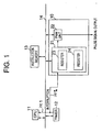
- Fig.1 is a block diagram of a PWM system according to the present invention.
- the system of Fig.1 includes a PWM apparatus 10, a CPU 11, a timer 12, an instruction memory 13, and a CPU bus 14.
- the PWM apparatus 10, the CPU 11, the timer 12, and the instruction memory 13 are connected together via the CPU bus 14.
- the CPU 11 operates based on programs that are a series of instructions stored in the instruction memory 13.
- the timer 12 is controlled by the CPU 11, for example, via the CPU bus 14, and marks time by counting clock pulses or the like.
- the timer 12 When detecting an arrival of a preset time such as at an end of a predetermined time interval, the timer 12 generates an interruption signal.
- the interruption signal is supplied to the CPU 11 via an interruption signal line int1 and to the PWM apparatus 10 via an interruption signal line int2.
- the PWM apparatus 10 is connected to the CPU bus 14, and is controlled by the CPU 11. Further, the PWM apparatus 10 receives the interruption signal from the timer 12 via the interruption signal line int2.
- the PWM apparatus 10 includes a PWM unit 22 and a control unit 21 where the PWM unit 22 has substantially the same configuration as a conventional PWM unit, and the control unit 21 includes registers 23 and 24.
- the control unit 21 receives the interruption signal from the timer 12 via the interruption signal line int2, and, in response, supplies a duty setting and a cycle setting stored in the respective registers 23 and 24 to the PWM unit 22.
- the PWM unit 22 stores the received duty setting and cycle setting in internal registers, and outputs a pulse signal in accordance with the renewed settings. With this, the output pulse signal is changed from an old PWM waveform to a new PWM waveform.
- the CPU 11 Upon receiving an interruption signal from the timer 12 through the interruption signal line int1, the CPU 11 obtains a duty ratio and a cycle for a next PWM waveform, for example, based on computation or data stored in a memory.
- the CPU 11 supplies the duty ratio and the cycle to the PWM apparatus 10 through the CPU bus 14.
- the transferred duty ratio and cycle are stored in the respective registers 23 and 24 of the control unit 21 as a duty ratio and a cycle for a next PWM waveform, for example.
- the duty ratio and cycle that are stored in the respective registers 23 and 24 in response to the interruption from the timer 12 to the CPU 11 are provided as preparation for an immediately following interruption, for example.
- the registers 23 and 24 may be implemented by using FIFOs or sets of registers.
- the CPU 11 responds to the interruption sent from the timer 12 via the interruption signal line int1 by supplying a duty ratio and a cycle that are to be used for a second next interruption, a third next interruption, etc., in stead of a next and immediately following interruption.
- the registers 23 and 24 may not be registers each for storing a single piece of data therein, but may serve as register queues for storing a series of data pieces such as next data, second next data, third next data, and so on.
- the CPU 11 can generate next data reliably prior to a next event of interruption and can supply the data to the PWM apparatus 10, there is not necessarily a need to await an interruption signal supplied from the timer 12 via the interruption signal line int1 before supplying data. Further, if register queues are employed, and if it is possible for the CPU 11 to compute data for future needs beforehand, the CPU 11 may compute data for next ten interruptions, for example, and may supply the data through the CPU bus 14 to the PWM apparatus 10, thereby storing the data for the next ten interruptions in the register queues at once.
- the interruption signal from the timer 12 is directly supplied to the PWM apparatus 10.
- the PWM apparatus 10 supplies settings such as the duty setting and the cycle setting stored in the registers to the PWM unit 22, which is used to actually generate a pulse signal. This achieves a change in the PWM waveform of the output pulse signal. In this manner, it is possible to modify the PWM waveform at a desired timing indicated by an external event such as a trigger from the timer 12.
- the settings such as the duty setting and the cycle setting stored in the registers of the PWM apparatus 10 are supplied from the CPU 11 to the PWM apparatus 10 via the CPU bus 14 in response to an interruption signal issued by the timer 12, for example.
- the settings of data may be made successively for the immediately following interruption, or may be made at once with respect to data for a plurality of future interruptions.
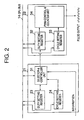
- Fig.2 is a block diagram of a first embodiment of the PWM apparatus 10 according to the present invention.
- the same elements as those of Fig.1 are referred to by the same numerals, and a description thereof will be omitted.
- the control unit 21 includes the duty setting register 23 and the cycle setting register 24. Further, the control unit 21 includes a selector-&-controller unit 31.
- the duty setting register 23 and the cycle setting register 24 are directly connected to the CPU bus 14, and receive duty data and cycle data, respectively, from the CPU 11 through the CPU bus 14.
- the CPU bus 14 includes an address bus, a data bus, and a control signal bus for conveying a chip selecting signal, a read/write signal, and the like.
- the selector-&-controller unit 31 receives control signals from the control signal bus, and controls data write/read operations in respect of the duty setting register 23 and the cycle setting register 24 in accordance with the received control signals. Further, the selector-&-controller unit 31 receives an interruption signal from the timer 12, and controls data transfer operations for transferring data from the duty setting register 23 and the cycle setting register 24 to the PWM unit 22 in accordance with the received interruption signal.
- the PWM unit 22 includes a duty setting register 32, a cycle setting register 33, and a PWM-control-&-counter unit 34.
- the duty setting register 32 and the cycle setting register 33 are directly connected to the CPU bus 14.
- the PWM-control-&-counter unit 34 operates as a unit that generates a pulse signal, and generates a pulse signal in accordance with the data stored in the duty setting register 32 and the cycle setting register 33, thereby outputting the pulse signal to the exterior of the device.
- the PWM unit 22 has substantially the same configuration as a conventional PWM apparatus, and is capable of modifying the PWM waveform of the pulse signal output under the control of the CPU in accordance with the data stored in the duty setting register 32 and the cycle setting register 33 in the same manner as in the conventional art.
- the PWM unit 22 is additionally configured such that the duty setting register 32 allows data thereof to be written by the selector-&-controller unit 31.
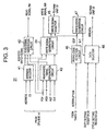
- Fig.3 is a block diagram showing a example configuration of the selector-&-controller unit 31.
- the selector-&-controller unit 31 includes an address decoder 41, a read-signal generation circuit 42, a read/write-timing generation circuit 43, a write-signal generation circuit 44, a write-signal selector 45, a rising-edge detection circuit 46, a write-state generation circuit 47, and a data selector 48.
- Fig.4 is a timing chart for explaining operations of the selector-&-controller unit 31 of Fig.3 when data is written in and read from the duty setting register 23 and the cycle setting register 24. In the following, data read/write operations with respect to the register queues will be described with reference to Fig.2, Fig.3, and Fig.4.
- control signals are supplied from the CPU 11 to the selector-&-controller unit 31 of the control unit 21 through the CPU bus 14.
- These control signals include a chip selecting signal CS, a read signal RDX, a write signal WRX, a reset signal RST, and a clock signal CLK.
- the chip selecting signal CS is supplied to the address decoder 41.
- the read signal RDX, the write signal WRX, the reset signal RST, and the clock signal CLK are supplied to the read/write-timing generation circuit 43.
- Address signals are conveyed through the address bus of the CPU bus 14 in synchronization with the chip selecting signal CS, and are supplied to the address decoder 41.
- (a) through (f) show timing relations between these signals.
- the address decoder 41 receives the address signals in addition to the chip selecting signal CS, and decodes the received address.
- the address decoder 41 generates an address match signal as shown in (f) of Fig.4 when the chip selecting signal CS selects this chip among other chips while the received address matches an address of the register of the PWM apparatus 10.
- the address match signal is supplied to the read-signal generation circuit 42 and the write-signal generation circuit 44.
- the read/write-timing generation circuit 43 Based on the clock signal CLK, the read/write-timing generation circuit 43 generates a read timing signal indicative of a timing of a read operation, and generates a write timing signal indicative of a timing of a write operation.
- the read timing signal is supplied to the read-signal generation circuit 42, and the write timing signal is supplied to the write-signal generation circuit 44.
- the read-signal generation circuit 42 generates a read signal RD (as shown in Fig.4, (i)) at a timing specified by the read timing signal when the read signal RDX indicates a read operation while the address match signal is activated.
- the write-signal generation circuit 44 generates a write signal WR (as shown in Fig.4, (j)) at a timing specified by the write timing signal when the write signal WRX indicates a write operation whilst the address match signal is activated.
- These read signal RD and write signal WR are supplied to the duty setting register 23 and the cycle setting register 24, thereby ordering a read operation and a write operation in respect of these registers.
- the read signal RD orders a read operation
- data is read from the register of an indicated address, and is output to the data bus of the CPU bus 14.
- the write signal WR orders a write operation
- data conveyed through the data bus of the CPU bus 14 is written in the register queue at an indicated address.
- the data signal of the data bus is shown in Fig.4, (g).
- the CPU 11 carries out a data write operation and a data read operation in respect of the duty setting register 23 and the cycle setting register 24 of the control unit 21.
- the CPU 11 may perform a data write operation and a data read operation with respect to the duty setting register 32 and the cycle setting register 33 of the PWM unit 22.
- Fig.5 is a timing chart for explaining operations performed by the selector-&-controller unit 31 when the timer 12 generates an interruption signal. Operations of modifying the waveform of a pulse signal will be described with reference to Fig.2, Fig.3, and Fig.5.
- the interruption signal generated by the timer 12 arrives at the selector-&-controller unit 31 of the control unit 21.
- the interruption signal arriving at the selector-&-controller unit 31 is supplied to the rising-edge detection circuit 46.
- the rising-edge detection circuit 46 detects a rising edge of the interruption signal to generate a rising edge pulse EGP.
- the rising edge pulse EGP is supplied to the write-signal selector 45 and the write-state generation circuit 47.
- the write-signal selector 45 In response to the rising edge pulse EGP, the write-signal selector 45 generates write signals PWMWR respectively for the cycle setting purpose and for the duty setting purpose, and these generated signals are supplied to the PWM unit 22.
- the write-state generation circuit 47 responsive to the rising edge pulse EGP, changes an internal state thereof, and generates a selection signal SLT accordingly.
- the selection signal SLT is supplied to the data selector 48.
- the interruption signal, the rising edge pulse EGP, the internal state of the write-state generation circuit 47, the write signal PWMWR for the cycle setting, the write signal PWMWR for the duty setting, and the selection signal SLT described above are shown in Fig.5, (a) through (f), respectively.
- the data selector 48 selects data of a register indicated by the selection signal SLT.
- the selection signal SLT is HIGH, for example, data of the cycle setting register 24 is selected.
- the selection signal is LOW, on the other hand, data of the duty setting register 23 is selected.
- the selection signal SLT is HIGH when the data of the cycle setting register 24 is to be selected, and is LOW when the data of the duty setting register 23 is to be selected.
- the write data WRDATA (Fig.5, (i)) supplied to the PWM unit 22 turns into data CYCLE#00 that is the first data of the cycle setting register 24.
- the write data WRDATA (Fig.5, (i)) supplied to the PWM unit 22 turns into data DUTY#00 that is the first data of the duty setting register 23.
- the data CYCLE#00 of the write data WRDATA that is the first data of the cycle setting register 24 is stored in the cycle setting register 33 in response to the write signal PWMWR for the cycle setting (Fig.5, (d)).
- the data DUTY#00 of the write data WRDATA that is the first data of the duty setting register 23 is stored in the duty setting register 32 in response to the write signal PWMWR for the duty setting (Fig.5, (e)).
- the configuration of Fig.2 is designed such that data for cycle setting is temporarily stored in the duty setting register 32 first, and, then, is transferred from the duty setting register 32 to the cycle setting register 33.
- the data of the cycle setting register 24 is updated to the second data (#01) after the first data (#00) is read therefrom.
- writing of data in the cycle setting register 24 is carried out in the manner as described with reference to the Fig.4.
- the data of the duty setting register 23 is updated to the second data (#01) after the first data (#00) is read therefrom. Writing of data in the duty setting register 23 in this regard is carried out in the manner as described with reference to the Fig.4.
- an interruption signal from the timer 12 is directly supplied to the PWM apparatus 10.
- the PWM apparatus 10 supplies settings such as the duty setting and the cycle setting stored in the registers to the PWM unit 22, which is used to actually generate a pulse signal. This achieves a change in the PWM waveform of the output pulse signal.
- the settings such as the duty setting and the cycle setting stored in the registers of the PWM apparatus 10 are supplied from the CPU 11 to the PWM apparatus 10 via the CPU bus 14 in response to an interruption signal issued by the timer 12, for example.
- the setting of data is made successively for the immediately following interruption.
- Fig. 6 is a block diagram of a second embodiment of the PWM apparatus 10 according to the present invention.
- the same elements as those of Fig.2 are referred to by the same numerals, and a description thereof will be omitted.
- setting of data by the CPU is directed to data for the next and immediately following interruption.
- the second embodiment is configured such that data for a plurality of future interruptions are stored at once or successively in advance.
- the second embodiment of Fig.6 has a duty setting register queue 23A and a cycle setting register queue 24A, which replace the duty setting register 23 and the cycle setting register 24, respectively.
- the duty setting register queue 23A and the cycle setting register queue 24A may each be comprised of a FIFO (first-in first-out) or the like from which data is successively read in the same order as the data is successively stored. In this case, not only data for the next interruption but also data for the second next interruption, data for the third next interruption, etc., may be computed while there is no other load on the CPU 11, for example, and are stored in the duty setting register queue 23A and the cycle setting register queue 24A at once or successively in advance.
- FIFO first-in first-out
- the duty setting register queue 23A and the cycle setting register queue 24A may each be comprised of a set of registers having respective addresses assigned thereto.
- data for the next interruption but also data for the second next interruption, data for the third next interruption, etc. may be computed while there is no other load on the CPU 11, for example, and are stored in the duty setting register queue 23A and the cycle setting register queue 24A at once or successively in advance.
- data can be written by indicating a writing address. Because of this, after writing data for ten future interruptions, the data for the sixth through tenth future interruptions can be changed, for example, by specifying respective addresses if data changes become necessary upon situational changes.
- data that is supplied from the duty setting register queue 23A and the cycle setting register queue 24A to the PWM unit 22 by the selector-&-controller unit 31 is the data that is successively output from the FIFOs.
- means to indicate an address of next data may be provided by a counter or the like, and data of the register indicated by this address indicating means may be supplied successively from the duty setting register queue 23A and the cycle setting register queue 24A to the PWM unit 22.
- an external event for triggering modification of the pulse signal waveform is an event of a timer.
- the external event is not limited to an even of a timer, but may include a signal that is supplied from an exterior of the system when a predetermined status or an interruption signal from an input/output interface is detected. Also, the external event may not be a periodic event, but may be a trigger that takes place at any timing.
Landscapes
- Engineering & Computer Science (AREA)
- Theoretical Computer Science (AREA)
- Physics & Mathematics (AREA)
- General Engineering & Computer Science (AREA)
- General Physics & Mathematics (AREA)
- Inverter Devices (AREA)
- Analogue/Digital Conversion (AREA)
- Control Of Stepping Motors (AREA)
- Control Or Security For Electrophotography (AREA)
Claims (9)
- Dispositif destiné à gérer un signal impulsionnel, comprenant :au moins un premier registre (23) qui mémorise des données de forme d'onde dans celui-ci, etune unité de génération de signal impulsionnel (22) qui génère un signal impulsionnel conformément aux données de forme d'onde dudit premier registre (23),caractérisé par :une unité de commande (21) qui est connectée à un bus (14) et est commandée par des signaux de commande fournis depuis le bus (14), etune ligne de signaux (int 2) qui est séparée et indépendante du bus (14), et est connectée à ladite unité de commande (21), où ladite unité de commande (21) extrait des données de mise à jour pour ledit premier registre (23) à partir dudit bus (14) sur la base dudit signal de commande et met à jour les données de forme d'onde dudit premier registre (23) avec les données de mise à jour en réponse à un signal qui est fourni de l'extérieur par l'intermédiaire de ladite ligne de signaux (int 2), lesdites données de mise à jour comprenant des données indicatives d'une période du signal impulsionnel et des données indicatives d'un rapport cyclique du signal impulsionnel.
- Dispositif selon la revendication 1, dans lequel ladite unité de commande (21) comprend :un second registre (24), etun contrôleur (31) qui mémorise des nouvelles données de forme d'onde dans ledit second registre (24) conformément aux signaux de commande fournis depuis le bus (14), et transfère les nouvelles données de forme d'onde dudit second registre (24) audit premier registre (23) en réponse au signal qui est fourni depuis l'extérieur par l'intermédiaire de ladite ligne de signaux (int 2).
- Dispositif selon la revendication 2, dans lequel ledit second registre (24) est une file d'attente de registre qui mémorise dans celle-ci une pluralité d'éléments de données de forme d'onde correspondant à une pluralité de mises à jour des données de forme d'onde mémorisées dans ledit premier registre (23).
- Dispositif selon la revendication 3, dans lequel ladite file d'attente de registre est un ensemble de registres comportant des adresses respectives affectées à ceux-ci.
- Dispositif selon la revendication 1, dans lequel ledit premier registre (23) est connecté au bus (14) et peut mémoriser dans celui-ci des données de forme d'onde qui sont fournies directement à partir du bus (14).
- Dispositif selon la revendication 1, comprenant en outre une unité centrale UC (11), ladite unité de commande (21) étant commandée par ladite unité UC (11).
- Dispositif selon la revendication 6, dans lequel ladite unité de commande (21) comprend :un second registre (24), etun contrôleur (31) qui mémorise de nouvelles données de forme d'onde dans ledit second registre (24) conformément à la commande par ladite unité UC (11), et qui transfère les nouvelles données de forme d'onde depuis ledit second registre (24) vers ledit premier registre (23) en réponse au signal fourni par l'intermédiaire de ladite ligne de signaux (int 2).
- Dispositif selon la revendication 7, dans lequel ladite ligne de signaux (int 2) est en outre connectée à ladite unité UC (11) en tant que ligne de signaux d'interruption (int 2).
- Dispositif selon la revendication 8, dans lequel ladite unité UC (11) commande ledit contrôleur (31) pour mémoriser les nouvelles données de forme d'onde dans ledit second registre (24) en réponse à un signal d'interruption fourni par l'intermédiaire de la ligne de signaux d'interruption (int 2).
Applications Claiming Priority (2)
| Application Number | Priority Date | Filing Date | Title |
|---|---|---|---|
| JP2000346981 | 2000-11-14 | ||
| JP2000346981A JP3987277B2 (ja) | 2000-11-14 | 2000-11-14 | パルス信号生成装置 |
Publications (2)
| Publication Number | Publication Date |
|---|---|
| EP1209810A1 EP1209810A1 (fr) | 2002-05-29 |
| EP1209810B1 true EP1209810B1 (fr) | 2006-08-30 |
Family
ID=18820777
Family Applications (1)
| Application Number | Title | Priority Date | Filing Date |
|---|---|---|---|
| EP01309477A Expired - Lifetime EP1209810B1 (fr) | 2000-11-14 | 2001-11-09 | Modulateur de durée d'impulsion répondant aux signaux externes |
Country Status (6)
| Country | Link |
|---|---|
| US (1) | US6862483B2 (fr) |
| EP (1) | EP1209810B1 (fr) |
| JP (1) | JP3987277B2 (fr) |
| CN (1) | CN1166059C (fr) |
| DE (1) | DE60122655T2 (fr) |
| TW (1) | TW559693B (fr) |
Families Citing this family (11)
| Publication number | Priority date | Publication date | Assignee | Title |
|---|---|---|---|---|
| US7200173B2 (en) * | 2003-10-27 | 2007-04-03 | Tushar Prakash Ringe | Method and apparatus for generating a distortionless pulse width modulated waveform |
| KR100787231B1 (ko) * | 2005-04-23 | 2007-12-21 | 삼성전자주식회사 | 고전압 발생장치, 고전압 발생방법 및 asic 칩 |
| US20090114526A1 (en) * | 2006-12-11 | 2009-05-07 | Huping Hu | Method and apparatus for producing non-local physical, chemical and biological effects |
| DE102007044803B4 (de) * | 2007-09-20 | 2025-08-14 | Robert Bosch Gmbh | Schaltungsanordnung zur Signalaufnahme und -erzeugung sowie Verfahren zum Betreiben dieser Schaltungsanordnung |
| WO2013029867A2 (fr) | 2011-08-26 | 2013-03-07 | Siemens Aktiengesellschaft | Procédé de génération d'une séquence de signaux d'impulsions |
| CN103401540B (zh) * | 2013-08-19 | 2016-03-30 | 西北师范大学 | 基于tms320vc5402芯片的可编程脉宽调制产生器 |
| GB2539459A (en) * | 2015-06-16 | 2016-12-21 | Nordic Semiconductor Asa | Waveform generation |
| CN105224481A (zh) * | 2015-10-22 | 2016-01-06 | 福州瑞芯微电子股份有限公司 | Pwm在输入模式下传输数据的实现方式 |
| CN106339027A (zh) * | 2016-09-08 | 2017-01-18 | 合肥迈威德智能科技有限公司 | 一种脉冲信号发生器 |
| JP2020077276A (ja) * | 2018-11-09 | 2020-05-21 | ルネサスエレクトロニクス株式会社 | 半導体装置、制御装置および制御方法 |
| CN118870600B (zh) * | 2024-09-27 | 2025-02-18 | 嘉兴汉微半导体有限公司 | 脉冲信号生成装置及方法 |
Family Cites Families (8)
| Publication number | Priority date | Publication date | Assignee | Title |
|---|---|---|---|---|
| JP3100148B2 (ja) * | 1990-07-03 | 2000-10-16 | 三菱電機株式会社 | 正弦波近似パルス幅変調信号発生装置 |
| US5598552A (en) * | 1991-04-17 | 1997-01-28 | Sierra Semiconductor Corporation | Error free data transfers |
| EP0579857A1 (fr) * | 1992-07-23 | 1994-01-26 | International Business Machines Corporation | Méthode pour générer des intervals d'impulsions successives avec ordinateur ayant des intervals d'impulsions qui sont en partie répétitives |
| JP2816389B2 (ja) * | 1992-10-05 | 1998-10-27 | 三菱電機株式会社 | パルス幅変調器 |
| US5416434A (en) * | 1993-03-05 | 1995-05-16 | Hewlett-Packard Corporation | Adaptive clock generation with pseudo random variation |
| CA2137509A1 (fr) | 1993-12-09 | 1995-06-10 | Young W. Lee | Circuit de modulation d'impulsions multiples en duree |
| DE4403732C1 (de) | 1994-02-07 | 1995-10-12 | Siemens Ag | Schaltungsanordnung zur Erzeugung pulsweiten modulierter Ausgangssignale oder zur Messung vom Impulsflankenabständen von Eingangssignalen |
| US6396317B1 (en) * | 1999-05-28 | 2002-05-28 | Peco Ii, Inc., | Digital voltage controlled oscillator |
-
2000
- 2000-11-14 JP JP2000346981A patent/JP3987277B2/ja not_active Expired - Fee Related
-
2001
- 2001-03-23 US US09/814,758 patent/US6862483B2/en not_active Expired - Fee Related
- 2001-11-09 DE DE60122655T patent/DE60122655T2/de not_active Expired - Lifetime
- 2001-11-09 EP EP01309477A patent/EP1209810B1/fr not_active Expired - Lifetime
- 2001-11-13 TW TW090128099A patent/TW559693B/zh not_active IP Right Cessation
- 2001-11-14 CN CNB011384875A patent/CN1166059C/zh not_active Expired - Fee Related
Also Published As
| Publication number | Publication date |
|---|---|
| DE60122655T2 (de) | 2006-12-21 |
| TW559693B (en) | 2003-11-01 |
| DE60122655D1 (de) | 2006-10-12 |
| US20020059004A1 (en) | 2002-05-16 |
| EP1209810A1 (fr) | 2002-05-29 |
| JP2002152020A (ja) | 2002-05-24 |
| US6862483B2 (en) | 2005-03-01 |
| CN1166059C (zh) | 2004-09-08 |
| JP3987277B2 (ja) | 2007-10-03 |
| CN1353503A (zh) | 2002-06-12 |
Similar Documents
| Publication | Publication Date | Title |
|---|---|---|
| EP1209810B1 (fr) | Modulateur de durée d'impulsion répondant aux signaux externes | |
| US5761522A (en) | Program control system programmable to selectively execute a plurality of programs | |
| US20060047754A1 (en) | Mailbox interface between processors | |
| KR20080023658A (ko) | 신호처리 파이프라인에서 버스트 데이터를 조절하기 위한장치 및 방법 | |
| KR20200110219A (ko) | 직렬 주변기기 인터페이스 마스터 | |
| US12124398B2 (en) | Input/output unit for data acquisition with a field-bus system | |
| EP1016965A1 (fr) | Système de gestion d'interruptions | |
| US7096295B2 (en) | Method and device for generating program interruptions in users of a bus system, and bus system | |
| US8131388B2 (en) | Electronic controller for power converter and motor drive circuit | |
| US5134562A (en) | Fifo register device adaptively changing a stage number in dependency on a bus cycle | |
| US6216217B1 (en) | Data processor | |
| US7663964B2 (en) | Memory device, memory system and method of operating such | |
| US7633814B2 (en) | Memory device and method of operating such | |
| US10181353B2 (en) | Memory control circuit and method thereof | |
| US6784929B1 (en) | Universal two dimensional (frame and line) timing generator | |
| EP0840237B1 (fr) | Synchronisation de processeur avec bus externe | |
| CN1308424A (zh) | 数字无绳电信系统终端的控制单元及用于控制单元的方法 | |
| US6684271B1 (en) | Method and apparatus for changing context in link channelization | |
| US6744833B1 (en) | Data resynchronization between modules sharing a common clock | |
| US5802595A (en) | Serial data transfer apparatus | |
| US6721897B1 (en) | Bus control circuit effecting timing control using cycle registers for respective cycles holding signal levels corresponding to bus control signals that are output by arrangement of signal level | |
| KR100192541B1 (ko) | 타이머 | |
| SU1140126A1 (ru) | Микропроцессор | |
| JPS6236933A (ja) | フレ−ム位相補正回路 | |
| JPH05276177A (ja) | ローカルエリアネットワークシステム |
Legal Events
| Date | Code | Title | Description |
|---|---|---|---|
| PUAI | Public reference made under article 153(3) epc to a published international application that has entered the european phase |
Free format text: ORIGINAL CODE: 0009012 |
|
| AK | Designated contracting states |
Kind code of ref document: A1 Designated state(s): AT BE CH CY DE DK ES FI FR GB GR IE IT LI LU MC NL PT SE TR |
|
| AX | Request for extension of the european patent |
Free format text: AL;LT;LV;MK;RO;SI |
|
| 17P | Request for examination filed |
Effective date: 20021105 |
|
| AKX | Designation fees paid |
Designated state(s): DE FR GB |
|
| 17Q | First examination report despatched |
Effective date: 20040422 |
|
| GRAP | Despatch of communication of intention to grant a patent |
Free format text: ORIGINAL CODE: EPIDOSNIGR1 |
|
| GRAS | Grant fee paid |
Free format text: ORIGINAL CODE: EPIDOSNIGR3 |
|
| GRAA | (expected) grant |
Free format text: ORIGINAL CODE: 0009210 |
|
| AK | Designated contracting states |
Kind code of ref document: B1 Designated state(s): DE FR GB |
|
| REG | Reference to a national code |
Ref country code: GB Ref legal event code: FG4D |
|
| REF | Corresponds to: |
Ref document number: 60122655 Country of ref document: DE Date of ref document: 20061012 Kind code of ref document: P |
|
| ET | Fr: translation filed | ||
| PLBE | No opposition filed within time limit |
Free format text: ORIGINAL CODE: 0009261 |
|
| STAA | Information on the status of an ep patent application or granted ep patent |
Free format text: STATUS: NO OPPOSITION FILED WITHIN TIME LIMIT |
|
| 26N | No opposition filed |
Effective date: 20070531 |
|
| REG | Reference to a national code |
Ref country code: GB Ref legal event code: 732E |
|
| REG | Reference to a national code |
Ref country code: FR Ref legal event code: TP |
|
| PGFP | Annual fee paid to national office [announced via postgrant information from national office to epo] |
Ref country code: FR Payment date: 20091123 Year of fee payment: 9 Ref country code: GB Payment date: 20091104 Year of fee payment: 9 |
|
| GBPC | Gb: european patent ceased through non-payment of renewal fee |
Effective date: 20101109 |
|
| REG | Reference to a national code |
Ref country code: FR Ref legal event code: ST Effective date: 20110801 |
|
| PG25 | Lapsed in a contracting state [announced via postgrant information from national office to epo] |
Ref country code: FR Free format text: LAPSE BECAUSE OF NON-PAYMENT OF DUE FEES Effective date: 20101130 |
|
| PG25 | Lapsed in a contracting state [announced via postgrant information from national office to epo] |
Ref country code: GB Free format text: LAPSE BECAUSE OF NON-PAYMENT OF DUE FEES Effective date: 20101109 |
|
| REG | Reference to a national code |
Ref country code: DE Ref legal event code: R082 Ref document number: 60122655 Country of ref document: DE Representative=s name: REICHERT & LINDNER PARTNERSCHAFT PATENTANWAELT, DE |
|
| REG | Reference to a national code |
Ref country code: DE Ref legal event code: R082 Ref document number: 60122655 Country of ref document: DE Representative=s name: REICHERT & LINDNER PARTNERSCHAFT PATENTANWAELT, DE Effective date: 20150512 Ref country code: DE Ref legal event code: R081 Ref document number: 60122655 Country of ref document: DE Owner name: SOCIONEXT INC., YOKOHAMA-SHI, JP Free format text: FORMER OWNER: FUJITSU SEMICONDUCTOR LTD., YOKOHAMA, KANAGAWA, JP Effective date: 20150512 |
|
| PGFP | Annual fee paid to national office [announced via postgrant information from national office to epo] |
Ref country code: DE Payment date: 20151103 Year of fee payment: 15 |
|
| REG | Reference to a national code |
Ref country code: DE Ref legal event code: R119 Ref document number: 60122655 Country of ref document: DE |
|
| PG25 | Lapsed in a contracting state [announced via postgrant information from national office to epo] |
Ref country code: DE Free format text: LAPSE BECAUSE OF NON-PAYMENT OF DUE FEES Effective date: 20170601 |