EP1217512A2 - Arithmetische Schaltung und arithmetisches Verfahren - Google Patents
Arithmetische Schaltung und arithmetisches Verfahren Download PDFInfo
- Publication number
- EP1217512A2 EP1217512A2 EP01128119A EP01128119A EP1217512A2 EP 1217512 A2 EP1217512 A2 EP 1217512A2 EP 01128119 A EP01128119 A EP 01128119A EP 01128119 A EP01128119 A EP 01128119A EP 1217512 A2 EP1217512 A2 EP 1217512A2
- Authority
- EP
- European Patent Office
- Prior art keywords
- memory
- register
- bits
- reading
- variable
- Prior art date
- Legal status (The legal status is an assumption and is not a legal conclusion. Google has not performed a legal analysis and makes no representation as to the accuracy of the status listed.)
- Granted
Links
Images


Classifications
-
- G—PHYSICS
- G06—COMPUTING OR CALCULATING; COUNTING
- G06F—ELECTRIC DIGITAL DATA PROCESSING
- G06F7/00—Methods or arrangements for processing data by operating upon the order or content of the data handled
- G06F7/38—Methods or arrangements for performing computations using exclusively denominational number representation, e.g. using binary, ternary, decimal representation
- G06F7/40—Methods or arrangements for performing computations using exclusively denominational number representation, e.g. using binary, ternary, decimal representation using contact-making devices, e.g. electromagnetic relay
- G06F7/44—Multiplying; Dividing
-
- G—PHYSICS
- G06—COMPUTING OR CALCULATING; COUNTING
- G06F—ELECTRIC DIGITAL DATA PROCESSING
- G06F9/00—Arrangements for program control, e.g. control units
- G06F9/06—Arrangements for program control, e.g. control units using stored programs, i.e. using an internal store of processing equipment to receive or retain programs
- G06F9/30—Arrangements for executing machine instructions, e.g. instruction decode
- G06F9/38—Concurrent instruction execution, e.g. pipeline or look ahead
- G06F9/3824—Operand accessing
-
- G—PHYSICS
- G06—COMPUTING OR CALCULATING; COUNTING
- G06F—ELECTRIC DIGITAL DATA PROCESSING
- G06F7/00—Methods or arrangements for processing data by operating upon the order or content of the data handled
- G06F7/60—Methods or arrangements for performing computations using a digital non-denominational number representation, i.e. number representation without radix; Computing devices using combinations of denominational and non-denominational quantity representations, e.g. using difunction pulse trains, STEELE computers, phase computers
- G06F7/72—Methods or arrangements for performing computations using a digital non-denominational number representation, i.e. number representation without radix; Computing devices using combinations of denominational and non-denominational quantity representations, e.g. using difunction pulse trains, STEELE computers, phase computers using residue arithmetic
- G06F7/728—Methods or arrangements for performing computations using a digital non-denominational number representation, i.e. number representation without radix; Computing devices using combinations of denominational and non-denominational quantity representations, e.g. using difunction pulse trains, STEELE computers, phase computers using residue arithmetic using Montgomery reduction
Definitions
- the present invention relates to an arithmetic circuit and an arithmetic method, and in particular to a speed increase for a preferable modular-multiplication for a public-key cryptosystem.
- public-key cryptography (asymmetrical cryptography) is employed to keep confidentiality of the information and for digital authentication purposes.
- Public-key cryptography is a cryptosystem for the transmission of information, a cryptography method for transmitting information using a pair of keys, consisting of a public key and a secret key.
- a sender uses the public key of a recipient to encrypt plaintext, and when the ciphertext is decrypted, a secret key known only to the recipient is used.
- the public-key cryptography since unlike the common-key cryptography (symmetrical cryptography) there is no need for correspondents to share and employ a single common key, and since widespread disclosure of a public key involves no appreciable risk, the maintenance of secrecy while communicating with an unlimited number of persons is possible.
- public-key cryptography is employed for digital authentication or to prepare a digital signature, the credibility and trustworthiness of a person with whom one is not acquainted can be established. Therefore, it can readily be asserted that public-key cryptography is a requisite technique for a network society supported by a communication system such as the Internet, and for business transactions that are entered into in such a network society.
- RSA is the most popular public-key cryptography. The safety afforded by RSA is based on a discrete logarithm problem for a very large integer, or on the difficulty encountered in factoring primes.
- SQRT is a function for providing a square root.
- the Montgomery multiplication method is a method for increasing the speed of the modular-squaring operation and the modular-multiplication operation in the above modular-exponentiation operation.
- the Montgomery multiplication method as described in "Modular Multiplication Without Trial Division", by Peter L. Montgomery, Mathematics of computations, Vol. 44, No. 170 April 1985, pp. 519-522, is a method whereby addition, multiplication and a shift operation are repeated to perform the modular-multiplication operation while requiring fewer calculations than are required by division for which subtraction is repetitively performed.
- the essential calculation portion P ⁇ XYR -1 (mod n) of the Montgomery multiplication is shown below using pseudo code 1.x.
- a product "t ⁇ n" is added each time to make p 0 equal to 0, where p 0 is the lowest block of the intermediate results P (line number 1.4).
- t is defined in line 1.3.
- X, Y and n are divided into m blocks, i.e.,
- variable p j , x i , y j , t and n j are r-bit length numbers
- variable c is a carry from a lower block.
- the addition of the 2r-bit length numbers x i ⁇ y j and t ⁇ n j and the addition of the r+1-bit length number p j and c are performed (line numbers 2.6 to 2.11), so that following the product addition the intermediate result tmp is a 2r+1-bit length number.
- the lower r bits of tmp are stored as variable p j
- the upper r+1 bits are stored as the variable c (line numbers 2.9 and 2.10).
- variable p j has the r-bit length
- variable tmp has the 2r-bit length
- the Montgomery multiplication can be performed in the manner as is shown in the pseudo codes 2.x and 3.x. However, through a detailed, careful study of the calculation cycle, the present inventors found that the performance of the calculation is greatly affected by the register allocation of the variables and the memory structure. The discussion results will now be described.
- the variable N having an r-bit length, is repetitively employed in the i-loop (pseudo code 2.2 to 2.13) without its value being changed, and variables t and x i are repetitively used in the j-loop (pseudo code 2.6 to 2.11) without their values being changed. Therefore, once the variables N, t and x i have been calculated or read from memory, they can be stored in the registers and repetitively employed until the loops are exited.
- the variables tmp and c that are used in the j-loop are directly allocated to the registers, and the other variables are stored in a general two-port memory wherein reading and writing to independent addresses can be performed.
- three cycles are required to read variables p 0 , x i and y 0 , other than the variable N that is allocated to the register.
- the variable t need not be read because, as is described above, the result obtained on line 2.3 is directly allocated for the register.
- the pseudo code 3.x example is more advantageous than is the pseudo code 2.x example because, even though many cycles are required, the carry is smaller than that of the pseudo code 2.x by one bit, and can be stored into the r-bit block, and less number of registers are required. Therefore, the pseudo code 3.x example is more advantageous with respect to complexity of control and the circuit size.
- Fig. 7 is a circuit diagram showing a Montgomery multiplier data path unit for the pseudo code 3.x
- variables that are required for an arithmetic operation performed during a single cycle and that must be read from memory can be stored in a different memory, and may be read at the same time during a single reading stage. In this manner, reading wait time can be minimised, and the performance of calculations can be improved. Furthermore, a complicated circuit or a circuit that requires a large hardware resource, such as a three-port memory, need not be employed as the memory used for storing variables, and instead, by employing a general-purpose memory having two ports or only a single port, an IP core can be easily formed, and the circuit size can be minimised.
- an arithmetic circuit comprises: multiple registers; an arithmetic unit, for regarding, as inputs, values entered in the multiple registers; and multiple memories, wherein the reading of multiple variables from the multiple memories to the multiple registers is performed during the same reading stage using a pipeline process performed by the arithmetic unit.
- an arithmetic method using an arithmetic circuit that includes an arithmetic unit, which has multiple input registers and multiple memories comprises the steps of: performing an arithmetic operation based on values stored in the input registers; writing the results of the arithmetic operation in the input registers or the memories; and reading multiple variables from the multiple memories and storing the variables in the multiple input registers during the same pipeline stage.
- the arithmetic unit can be a multiplier adder for, based on values x 1 , x 2 , x 3 and x 4 having an r-bit length that are respectively input to a first register, a second register, a third register and a fourth register, providing the operation results Q for x 1 + x 2 ⁇ x 3 + x 4 having a length of 2r bits or 2r+1 bits.
- the multiple memories include a first memory and a second memory.
- first memory and the second memory can be two-port memories having one data writing port and one data reading port, or the first memory can be a two-port memory having one data writing port and one data reading port, while the second memory can be a single-port memory having one port for the writing and reading of data.
- the arithmetic unit can be a multiplier adder for, based on values x 1 , x 2 , x 3 , x 4 x 5 and x 6 , having an r-bit length, that are respectively input to a first register, a second register, a third register, a fourth register, a fifth register and a sixth register, and for providing the operation results Q for x 1 + x 2 ⁇ x 3 + x 4 ⁇ x 5 + x 6 , which have a length of 2r bits or 2r+1 bits.
- the multiple memories include a first memory, a second memory and a third memory.
- the first memory can be a two-port memory having one data writing port and one data reading port
- the second memory and the third memories can be single-port memories having one port for the writing and the reading of data.
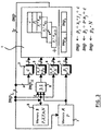
- Fig. 1 is a block diagram showing a data path section for an example Montgomery multiplier according to a first embodiment of the invention.
- the Montgomery multiplier in this embodiment comprises: a multiplier adder 1, input registers 2 to 5, a multiplexer 6, and two memories 7 and 8 (memory A and memory B).
- the multiplier adder 1 can be constituted by, for example, a well known full adder FA and half adder HA. In Fig. 1, a value, such as x i(0) , denotes a value obtained by extracting a bit that corresponds to the number in the parenthesis for a variable x i .
- the multiplexer 6 is a switch for receiving three inputs and providing one output.
- the memories 7 and 8 are general, two-port memories, i.e., memories for which data writing or data reading is performed by using one of two independent ports.
- An intermediate variable P(p j ) in the double loop process is recorded in the memory 7 (memory A), and other variables X(x i ), Y(y j ), n(n j ) and N and the final results P(p j ) are recorded in the memory 8 (memory B).
- the memories 7 and 8 are two-port memories, and do not constitute a barrier for the IP core formation, and do not increase the circuit area.
- the reading, computation and writing of data are performed as a pipeline operation. That is, the stage for reading data from the memories to the registers, the stage for the arithmetic operation based on the value input to the registers, and the stage for writing the operating results in the registers or the memories are performed in parallel.
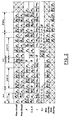
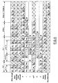
- Fig. 2 is a timing chart showing the timing for the process performed by the circuit in Fig. 1 for the pseudo code 3.x example.
- the pipeline process (the reading and computing of data and the writing of the results) is shown using grey or white to be represented with the same background colour.
- reading target memories MemA(read), MemB(read)
- registers p j (register 5), y j , n j and N (register 4), c (register 2), and x i and t (register 3)
- writing target memories MemA(write), MemB(write)
- data read from each memory at the reading stage, data loaded in each register at the operation stage, and data to be written at a writing stage are shown.
- the operation stage (calculation process on line 3.16) of the preceding cycle and the writing stage of its antecedent (the writing of p 2 to the memory 7 (MemA) and the writing of upper bits tmp H to the register c) are performed.
- p 4 is read from the memory 7 and is loaded in the register 5 (p j ), and this data is added to the data in the register c. The result is stored into the memory 7 as p 3 . It should be noted that in the memory writing process in the final i-loop, p j is stored not only in the memory 7 but also in the memory 8.
- the pseudo code 3.x example has been employed for the explanation of this embodiment; however, as is shown in the pseudo code 2.x example, x i ⁇ y j and t ⁇ n j can be added together during a single j-loop. Compared with the pseudo code 3.x, for the pseudo code 2.x the number of cycles spent waiting for the reading of the variable p j is reduced by about half, so that overall, the number of cycles is smaller. However, when the two memories are provided and are separately employed as in this embodiment, there is no difference in the effects obtained by the two pseudo codes. This is because, as is apparent from Fig. 2, p j and y j , or p j and n j can be read from the different memories at the same time, and there is no extra waiting time.
- the required number of cycles can be reduced to about 2/3 the conventional number, 3m 2 + 4m + 2. Further, since the bit length is not increased to r+1 bits by inducing an extra carry to P m-1 , an exception process is not required and the circuit structure can be simplified.
- Fig. 3 is a block diagram showing a data path section for an example Montgomery multiplier according to a second embodiment of the present invention.
- the arithmetic circuit in this embodiment is the same as in the first embodiment, except that a memory 8 (memory B) is a single-port memory, i.e., employs the same port both for data reading and data writing.
- a single-port memory is employed as the memory 8
- the memory size can be reduced, and accordingly, smaller circuit can be obtained.
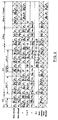
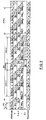
- Fig. 4 is a timing chart showing the timing of a process performed by the circuit in Fig. 3 for the pseudo code 3.x example.
- the process up until the i-loop is terminated is the same as the first embodiment.
- the final calculation result, p j is written in the memory 7 (MemA) instead of the memory 8.
- p j is transmitted from the memory 7 (MemA) to the memory 8 (MemB).
- both P and P-n are written to the memory 8 (MemB), and one of them is selected in accordance with the results of the subtraction, while in this embodiment, P and P-n are written only to the memory 7 (MemA), and one of them is written to the memory 8 (MemB) in accordance with the results of the subtraction.
- a single-port memory can be employed as the memory 8 (MemB), and the memory size can be reduced.
- the number of cycles required for this embodiment is 2m 2 + 5m + 3, whereas when the pseudo code 2.x is conventionally processed using the single-port memory, the number of cycles is 4m 2 + 5m + 2, and when the pseudo code 3.x is processed, the number of cycles required is 6m 2 + 7m + 2.
- the demonstrated superiority of the invention is even more outstanding.
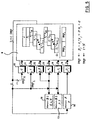
- Fig. 5 is a block diagram showing a data path section for an example Montgomery multiplier according to a third embodiment of the invention.
- the Montgomery multiplier of this embodiment includes a multiplier adder 9, input registers 10 to 15 and three memories 16, 17 and 18 (memory A, memory B1 and memory B2).
- the multiplier adder 9 adds the product of input values (r-bit lengths of the register 11 (t register) and the register 12 (n j , N register), the product of the input values (r-bit lengths) of the register 13 (x i register) and the register 14 (y j register), and the input value (r+1 bit length) of the register 10 (c register), and the input value (r-bit length) of the register 15 (p j register), and provides as output tmp, which has a 2r+1 bit length.
- the registers are the same as those in the first embodiment.
- the memory 16 (MemA) is a general two-port memory, and the memories 17 and 18 (MemB1 and B2) are single-port memories. Since these general memories are employed, the barrier to IP core formation is encountered, and the increase in the number of memories can be compensated for by a reduction of the circuit area occasioned by the employment of the single-port memories.
- the calculation of t (pseudo codes 2.3 and 2.4) is performed the first i-loop.
- P 0 is read from the memory 16
- x 3 is read from the memory 17
- y 0 is read from the memory 18.
- These data reading processes are performed during one reading stage.
- the operation on line 2.3 is performed using the variables that are read, and the lower bits tmp L of the calculation result are loaded in the t register.
- N is read from the memory 17, and the calculation on line 2.4 is performed using t and N.
- the lower bits tmp L of the operation result are loaded in the t register, and the value of t is employed throughout this loop.
- x 3 which was read previously, is also employed throughout the loop.
- the final, required number of cycles is m 2 + 5m + 2.
- m 2 greatly affects the number of required cycles, especially when the value of m is increased, the effects produced by this embodiment are still more outstanding.
- the circuit for this embodiment is employed, the bottleneck that is encountered during memory access when two multipliers are employed can be eliminated, and the number of required cycles can be considerably reduced.
- the specific effects obtained by the invention are as follows.
- the bottleneck encountered with the Montgomery multiplier when memory is accessed can be eliminated by using general two-port memories or single-port memories. And as a result, high-level performances can be attained while circuit sizes are reduced, and a low-cost cryptographic hardware can be provided.
Landscapes
- Engineering & Computer Science (AREA)
- Physics & Mathematics (AREA)
- General Physics & Mathematics (AREA)
- Theoretical Computer Science (AREA)
- Computational Mathematics (AREA)
- Mathematical Analysis (AREA)
- Mathematical Optimization (AREA)
- Pure & Applied Mathematics (AREA)
- General Engineering & Computer Science (AREA)
- Software Systems (AREA)
- Computing Systems (AREA)
- Mathematical Physics (AREA)
- Electromagnetism (AREA)
- Complex Calculations (AREA)
- Advance Control (AREA)
- Memory System (AREA)
Applications Claiming Priority (2)
| Application Number | Priority Date | Filing Date | Title |
|---|---|---|---|
| JP2000386069 | 2000-12-19 | ||
| JP2000386069A JP3709553B2 (ja) | 2000-12-19 | 2000-12-19 | 演算回路および演算方法 |
Publications (3)
| Publication Number | Publication Date |
|---|---|
| EP1217512A2 true EP1217512A2 (de) | 2002-06-26 |
| EP1217512A3 EP1217512A3 (de) | 2008-03-05 |
| EP1217512B1 EP1217512B1 (de) | 2009-08-19 |
Family
ID=18853225
Family Applications (1)
| Application Number | Title | Priority Date | Filing Date |
|---|---|---|---|
| EP01128119A Expired - Lifetime EP1217512B1 (de) | 2000-12-19 | 2001-11-27 | Arithmetische Schaltung und arithmetisches Verfahren |
Country Status (8)
| Country | Link |
|---|---|
| US (1) | US6772942B2 (de) |
| EP (1) | EP1217512B1 (de) |
| JP (1) | JP3709553B2 (de) |
| KR (1) | KR100441036B1 (de) |
| CN (1) | CN1221891C (de) |
| AT (1) | ATE440320T1 (de) |
| DE (1) | DE60139597D1 (de) |
| TW (1) | TW530260B (de) |
Cited By (1)
| Publication number | Priority date | Publication date | Assignee | Title |
|---|---|---|---|---|
| EP1560110A1 (de) * | 2004-01-26 | 2005-08-03 | Fujitsu Limited | Schaltung für die Mehrwort-Multiplikation/Akkumulation und Schaltung für die modulare Montgomery Multiplikation/Akkumulation |
Families Citing this family (19)
| Publication number | Priority date | Publication date | Assignee | Title |
|---|---|---|---|---|
| GB2404487A (en) * | 2003-07-31 | 2005-02-02 | Sony Uk Ltd | Access control for digital storage medium content |
| JP4544870B2 (ja) | 2004-01-26 | 2010-09-15 | 富士通セミコンダクター株式会社 | 演算回路装置 |
| JP4663421B2 (ja) * | 2005-06-24 | 2011-04-06 | 日本電信電話株式会社 | 離散対数演算装置、方法及びプログラム |
| US8028015B2 (en) * | 2007-08-10 | 2011-09-27 | Inside Contactless S.A. | Method and system for large number multiplication |
| JP5097138B2 (ja) | 2009-01-15 | 2012-12-12 | シャープ株式会社 | モンゴメリ乗算のための演算回路及び暗号回路 |
| CN101751242B (zh) * | 2009-12-22 | 2013-08-21 | 无锡中星微电子有限公司 | 一种数据处理方法及系统 |
| TW201217993A (en) * | 2010-10-20 | 2012-05-01 | Huafan University | employing operation on decomposed matrices to reduce operation amount for single matrix per unit time for light-weighting matrix operation process in simpler operation circuit |
| CN102360281B (zh) * | 2011-10-31 | 2014-04-02 | 中国人民解放军国防科学技术大学 | 用于微处理器的多功能定点乘加单元mac运算装置 |
| CN102999313B (zh) * | 2012-12-24 | 2016-01-20 | 飞天诚信科技股份有限公司 | 一种基于蒙哥马利模乘的数据处理方法 |
| KR101633960B1 (ko) | 2013-08-27 | 2016-06-27 | 배종훈 | 유아 세정보조기구 |
| JP6193699B2 (ja) * | 2013-09-27 | 2017-09-06 | 株式会社ソシオネクスト | 演算回路 |
| TWI549090B (zh) * | 2014-08-29 | 2016-09-11 | 華梵大學 | Portable sensing operation device |
| CN106156614B (zh) * | 2015-03-25 | 2018-12-28 | 北京南瑞智芯微电子科技有限公司 | 一种抵抗故障攻击的防护方法和装置 |
| IL239880B (en) * | 2015-07-09 | 2018-08-30 | Kaluzhny Uri | Simplified montgomery multiplication |
| TWI575924B (zh) * | 2015-10-06 | 2017-03-21 | 瑞昱半導體股份有限公司 | 解密裝置、方法及電路 |
| TWI580243B (zh) * | 2015-10-06 | 2017-04-21 | 瑞昱半導體股份有限公司 | 解密裝置、方法及電路 |
| US10534836B2 (en) * | 2016-12-06 | 2020-01-14 | Gsi Technology Inc. | Four steps associative full adder |
| CN109814838B (zh) * | 2019-03-28 | 2024-04-12 | 贵州华芯半导体技术有限公司 | 获取加解密运算中的中间结果组的方法、硬件装置和系统 |
| TWI817742B (zh) * | 2022-09-27 | 2023-10-01 | 熵碼科技股份有限公司 | 數值轉換方法及數值轉換系統 |
Citations (3)
| Publication number | Priority date | Publication date | Assignee | Title |
|---|---|---|---|---|
| GB2318890A (en) | 1996-10-31 | 1998-05-06 | Motorola Ltd | Co-processor for performing modular multiplication |
| WO1999027437A1 (en) | 1997-11-26 | 1999-06-03 | Atmel Corporation | Apparatus for multiprecision integer arithmetic |
| EP0947914A1 (de) | 1998-03-30 | 1999-10-06 | Rainbow Technologies Inc. | Vom Rechenaufwand her effizientes modulares Multiplikationsverfahren und Gerät |
Family Cites Families (21)
| Publication number | Priority date | Publication date | Assignee | Title |
|---|---|---|---|---|
| US3689893A (en) * | 1969-05-09 | 1972-09-05 | Olivetti & Co Spa | Accounting machine processor |
| US4539635A (en) * | 1980-02-11 | 1985-09-03 | At&T Bell Laboratories | Pipelined digital processor arranged for conditional operation |
| US4488252A (en) * | 1982-02-22 | 1984-12-11 | Raytheon Company | Floating point addition architecture |
| JPS6198476A (ja) * | 1984-10-19 | 1986-05-16 | Casio Comput Co Ltd | カードターミナル |
| US4985848A (en) * | 1987-09-14 | 1991-01-15 | Visual Information Technologies, Inc. | High speed image processing system using separate data processor and address generator |
| US5146592A (en) * | 1987-09-14 | 1992-09-08 | Visual Information Technologies, Inc. | High speed image processing computer with overlapping windows-div |
| US4955024A (en) * | 1987-09-14 | 1990-09-04 | Visual Information Technologies, Inc. | High speed image processing computer with error correction and logging |
| US4862407A (en) * | 1987-10-05 | 1989-08-29 | Motorola, Inc. | Digital signal processing apparatus |
| KR920006283B1 (ko) * | 1988-02-19 | 1992-08-03 | 미쯔비시덴끼 가부시끼가이샤 | 디지탈신호 처리방식 |
| US5337395A (en) * | 1991-04-08 | 1994-08-09 | International Business Machines Corporation | SPIN: a sequential pipeline neurocomputer |
| JP2906792B2 (ja) * | 1991-11-15 | 1999-06-21 | 日本電気株式会社 | ディジタルプロセッサ及びその制御方法 |
| US5260898A (en) * | 1992-03-13 | 1993-11-09 | Sun Microsystems, Inc. | Result cache for complex arithmetic units |
| JPH07253965A (ja) * | 1994-03-16 | 1995-10-03 | Fujitsu Ltd | 積和演算器 |
| KR0138859B1 (ko) * | 1994-12-06 | 1998-06-15 | 양승택 | 다중 명령어 다중 데이타형 신경망 전용 디지탈 어레이 프로세서 및 이를 이용해 구성된 시스템 |
| JPH0969061A (ja) * | 1995-08-30 | 1997-03-11 | Sony Corp | ビデオ信号用プロセツサ |
| DE69629495T2 (de) * | 1995-10-06 | 2004-06-09 | Advanced Micro Devices, Inc., Sunnyvale | Vereinheitlichter multifunktions-operationsverteiler für die ungeordnete befehlsexekution in einem superskalaren prozessor |
| WO1998018078A1 (fr) * | 1996-10-24 | 1998-04-30 | Mitsubishi Denki Kabushiki Kaisha | Micro-ordinateur dont la memoire et le processeur se trouvent sur une meme puce |
| JP3616897B2 (ja) * | 1998-01-27 | 2005-02-02 | 富士通株式会社 | モンゴメリ法による乗算剰余計算装置 |
| US5939693A (en) * | 1998-02-02 | 1999-08-17 | Motorola Inc. | Polynomial calculator device, and method therefor |
| JP3829504B2 (ja) * | 1998-02-16 | 2006-10-04 | 株式会社デンソー | 情報処理装置 |
| US6560754B1 (en) * | 1999-05-13 | 2003-05-06 | Arc International Plc | Method and apparatus for jump control in a pipelined processor |
-
2000
- 2000-12-19 JP JP2000386069A patent/JP3709553B2/ja not_active Expired - Fee Related
-
2001
- 2001-11-27 AT AT01128119T patent/ATE440320T1/de not_active IP Right Cessation
- 2001-11-27 EP EP01128119A patent/EP1217512B1/de not_active Expired - Lifetime
- 2001-11-27 DE DE60139597T patent/DE60139597D1/de not_active Expired - Lifetime
- 2001-12-06 KR KR10-2001-0077092A patent/KR100441036B1/ko not_active Expired - Fee Related
- 2001-12-10 TW TW090130566A patent/TW530260B/zh not_active IP Right Cessation
- 2001-12-18 US US10/023,147 patent/US6772942B2/en not_active Expired - Lifetime
- 2001-12-19 CN CNB011437383A patent/CN1221891C/zh not_active Expired - Lifetime
Patent Citations (3)
| Publication number | Priority date | Publication date | Assignee | Title |
|---|---|---|---|---|
| GB2318890A (en) | 1996-10-31 | 1998-05-06 | Motorola Ltd | Co-processor for performing modular multiplication |
| WO1999027437A1 (en) | 1997-11-26 | 1999-06-03 | Atmel Corporation | Apparatus for multiprecision integer arithmetic |
| EP0947914A1 (de) | 1998-03-30 | 1999-10-06 | Rainbow Technologies Inc. | Vom Rechenaufwand her effizientes modulares Multiplikationsverfahren und Gerät |
Non-Patent Citations (1)
| Title |
|---|
| DENG YULIANG ET AL.: "Implementation of RSA cryptoprocessor based on Montgomery algorithm", SOLID STATE AND INTEGRATED CIRCUIT TECHNOLOGY, 21 October 1998 (1998-10-21) |
Cited By (2)
| Publication number | Priority date | Publication date | Assignee | Title |
|---|---|---|---|---|
| EP1560110A1 (de) * | 2004-01-26 | 2005-08-03 | Fujitsu Limited | Schaltung für die Mehrwort-Multiplikation/Akkumulation und Schaltung für die modulare Montgomery Multiplikation/Akkumulation |
| US8078661B2 (en) | 2004-01-26 | 2011-12-13 | Fujitsu Semiconductor Limited | Multiple-word multiplication-accumulation circuit and montgomery modular multiplication-accumulation circuit |
Also Published As
| Publication number | Publication date |
|---|---|
| US6772942B2 (en) | 2004-08-10 |
| JP3709553B2 (ja) | 2005-10-26 |
| ATE440320T1 (de) | 2009-09-15 |
| EP1217512A3 (de) | 2008-03-05 |
| EP1217512B1 (de) | 2009-08-19 |
| TW530260B (en) | 2003-05-01 |
| KR100441036B1 (ko) | 2004-07-21 |
| KR20020050105A (ko) | 2002-06-26 |
| DE60139597D1 (de) | 2009-10-01 |
| CN1221891C (zh) | 2005-10-05 |
| US20020074391A1 (en) | 2002-06-20 |
| JP2002207589A (ja) | 2002-07-26 |
| CN1366234A (zh) | 2002-08-28 |
Similar Documents
| Publication | Publication Date | Title |
|---|---|---|
| US6772942B2 (en) | Arithmetic circuit to increase the speed of a modular multiplication for a public key system for encryption | |
| EP0801345B1 (de) | Schaltung für Modulo-Multiplikations- und Exponentiationsarithmetik | |
| US6151393A (en) | Device and method for modular multiplication | |
| JP2008293034A (ja) | タイミング攻撃を阻止する標準化されたモジュラべき乗を計算することにより復号メカニズムを実行する方法と装置 | |
| US20050165876A1 (en) | Multiple-word multiplication-accumulation circuit and Montgomery modular multiplication-accumulation circuit | |
| KR100442218B1 (ko) | 몽고메리의 알고리즘을 이용한 멱승 잉여 연산기 | |
| KR100457177B1 (ko) | 유한체 상의 두 원소의 곱을 구하는 직렬-병렬 곱셈기 | |
| Neiße et al. | Switching blindings with a view towards IDEA | |
| EP1818810B1 (de) | Schaltkreis und Verfahren zur Vervielfältigung langer ganzzahliger Werte | |
| US20060222175A1 (en) | Computation method, computing device and computer program | |
| KR100297110B1 (ko) | 모듈러곱셈기 | |
| KR20050064645A (ko) | 역원 계산 회로, 역원계산 방법 및 상기 역원계산 방법을실행시키기 위한 프로그램을 기록한 컴퓨터로 읽을 수있는 기록매체 | |
| CA2617389C (en) | Encryption processor with shared memory interconnect | |
| CN119496617A (zh) | 一种椭圆曲线安全标量乘设计方法及运算控制系统 | |
| KR20020071327A (ko) | 씨알티를 이용한 하이래딕스 알에스에이 모듈로 멱승 처리기 | |
| Faz-Hernández et al. | Efficient and Secure Algorithms for GLV-Based Scalar Multiplication and their Implementation on GLV-GLS Curves (or Keep Calm and Stay with One (and p> 3)) | |
| Ananyi | Design of a reconfigurable processor for elliptic curve cryptography over NIST prime fields | |
| Neiße et al. | Switching Blindings | |
| JP2006309201A (ja) | 楕円曲線暗号における多重スカラー倍計算装置、署名検証装置、及び、それらのプログラム。 | |
| CA2640641A1 (en) | Public key cryptography utilizing elliptic curves |
Legal Events
| Date | Code | Title | Description |
|---|---|---|---|
| PUAI | Public reference made under article 153(3) epc to a published international application that has entered the european phase |
Free format text: ORIGINAL CODE: 0009012 |
|
| AK | Designated contracting states |
Kind code of ref document: A2 Designated state(s): AT BE CH CY DE DK ES FI FR GB GR IE IT LI LU MC NL PT SE TR |
|
| AX | Request for extension of the european patent |
Free format text: AL;LT;LV;MK;RO;SI |
|
| PUAL | Search report despatched |
Free format text: ORIGINAL CODE: 0009013 |
|
| AK | Designated contracting states |
Kind code of ref document: A3 Designated state(s): AT BE CH CY DE DK ES FI FR GB GR IE IT LI LU MC NL PT SE TR |
|
| AX | Request for extension of the european patent |
Extension state: AL LT LV MK RO SI |
|
| 17P | Request for examination filed |
Effective date: 20080902 |
|
| GRAP | Despatch of communication of intention to grant a patent |
Free format text: ORIGINAL CODE: EPIDOSNIGR1 |
|
| GRAP | Despatch of communication of intention to grant a patent |
Free format text: ORIGINAL CODE: EPIDOSNIGR1 |
|
| AKX | Designation fees paid |
Designated state(s): AT BE CH CY DE DK ES FI FR GB GR IE IT LI LU MC NL PT SE TR |
|
| RIC1 | Information provided on ipc code assigned before grant |
Ipc: G06F 7/72 20060101AFI20081023BHEP Ipc: G06F 9/302 20060101ALI20081023BHEP Ipc: G06F 9/38 20060101ALI20081023BHEP |
|
| GRAS | Grant fee paid |
Free format text: ORIGINAL CODE: EPIDOSNIGR3 |
|
| 17Q | First examination report despatched |
Effective date: 20090226 |
|
| GRAA | (expected) grant |
Free format text: ORIGINAL CODE: 0009210 |
|
| AK | Designated contracting states |
Kind code of ref document: B1 Designated state(s): AT BE CH CY DE DK ES FI FR GB GR IE IT LI LU MC NL PT SE TR |
|
| REG | Reference to a national code |
Ref country code: GB Ref legal event code: FG4D |
|
| REG | Reference to a national code |
Ref country code: CH Ref legal event code: NV Representative=s name: IBM RESEARCH GMBH ZURICH RESEARCH LABORATORY INTEL Ref country code: CH Ref legal event code: EP |
|
| REG | Reference to a national code |
Ref country code: IE Ref legal event code: FG4D |
|
| REF | Corresponds to: |
Ref document number: 60139597 Country of ref document: DE Date of ref document: 20091001 Kind code of ref document: P |
|
| REG | Reference to a national code |
Ref country code: GB Ref legal event code: 746 Effective date: 20091009 |
|
| PG25 | Lapsed in a contracting state [announced via postgrant information from national office to epo] |
Ref country code: SE Free format text: LAPSE BECAUSE OF FAILURE TO SUBMIT A TRANSLATION OF THE DESCRIPTION OR TO PAY THE FEE WITHIN THE PRESCRIBED TIME-LIMIT Effective date: 20090819 Ref country code: AT Free format text: LAPSE BECAUSE OF FAILURE TO SUBMIT A TRANSLATION OF THE DESCRIPTION OR TO PAY THE FEE WITHIN THE PRESCRIBED TIME-LIMIT Effective date: 20090819 Ref country code: ES Free format text: LAPSE BECAUSE OF FAILURE TO SUBMIT A TRANSLATION OF THE DESCRIPTION OR TO PAY THE FEE WITHIN THE PRESCRIBED TIME-LIMIT Effective date: 20091130 Ref country code: FI Free format text: LAPSE BECAUSE OF FAILURE TO SUBMIT A TRANSLATION OF THE DESCRIPTION OR TO PAY THE FEE WITHIN THE PRESCRIBED TIME-LIMIT Effective date: 20090819 |
|
| NLV1 | Nl: lapsed or annulled due to failure to fulfill the requirements of art. 29p and 29m of the patents act | ||
| PG25 | Lapsed in a contracting state [announced via postgrant information from national office to epo] |
Ref country code: NL Free format text: LAPSE BECAUSE OF FAILURE TO SUBMIT A TRANSLATION OF THE DESCRIPTION OR TO PAY THE FEE WITHIN THE PRESCRIBED TIME-LIMIT Effective date: 20090819 |
|
| PG25 | Lapsed in a contracting state [announced via postgrant information from national office to epo] |
Ref country code: CY Free format text: LAPSE BECAUSE OF FAILURE TO SUBMIT A TRANSLATION OF THE DESCRIPTION OR TO PAY THE FEE WITHIN THE PRESCRIBED TIME-LIMIT Effective date: 20090819 Ref country code: PT Free format text: LAPSE BECAUSE OF FAILURE TO SUBMIT A TRANSLATION OF THE DESCRIPTION OR TO PAY THE FEE WITHIN THE PRESCRIBED TIME-LIMIT Effective date: 20091221 |
|
| PG25 | Lapsed in a contracting state [announced via postgrant information from national office to epo] |
Ref country code: DK Free format text: LAPSE BECAUSE OF FAILURE TO SUBMIT A TRANSLATION OF THE DESCRIPTION OR TO PAY THE FEE WITHIN THE PRESCRIBED TIME-LIMIT Effective date: 20090819 |
|
| PLBE | No opposition filed within time limit |
Free format text: ORIGINAL CODE: 0009261 |
|
| STAA | Information on the status of an ep patent application or granted ep patent |
Free format text: STATUS: NO OPPOSITION FILED WITHIN TIME LIMIT |
|
| PG25 | Lapsed in a contracting state [announced via postgrant information from national office to epo] |
Ref country code: MC Free format text: LAPSE BECAUSE OF NON-PAYMENT OF DUE FEES Effective date: 20091130 Ref country code: BE Free format text: LAPSE BECAUSE OF FAILURE TO SUBMIT A TRANSLATION OF THE DESCRIPTION OR TO PAY THE FEE WITHIN THE PRESCRIBED TIME-LIMIT Effective date: 20090819 |
|
| REG | Reference to a national code |
Ref country code: CH Ref legal event code: PL |
|
| 26N | No opposition filed |
Effective date: 20100520 |
|
| PG25 | Lapsed in a contracting state [announced via postgrant information from national office to epo] |
Ref country code: LI Free format text: LAPSE BECAUSE OF NON-PAYMENT OF DUE FEES Effective date: 20091130 Ref country code: GR Free format text: LAPSE BECAUSE OF FAILURE TO SUBMIT A TRANSLATION OF THE DESCRIPTION OR TO PAY THE FEE WITHIN THE PRESCRIBED TIME-LIMIT Effective date: 20091120 Ref country code: CH Free format text: LAPSE BECAUSE OF NON-PAYMENT OF DUE FEES Effective date: 20091130 Ref country code: IE Free format text: LAPSE BECAUSE OF NON-PAYMENT OF DUE FEES Effective date: 20091127 |
|
| PGFP | Annual fee paid to national office [announced via postgrant information from national office to epo] |
Ref country code: FR Payment date: 20101203 Year of fee payment: 10 |
|
| PG25 | Lapsed in a contracting state [announced via postgrant information from national office to epo] |
Ref country code: IT Free format text: LAPSE BECAUSE OF FAILURE TO SUBMIT A TRANSLATION OF THE DESCRIPTION OR TO PAY THE FEE WITHIN THE PRESCRIBED TIME-LIMIT Effective date: 20090819 |
|
| PG25 | Lapsed in a contracting state [announced via postgrant information from national office to epo] |
Ref country code: LU Free format text: LAPSE BECAUSE OF NON-PAYMENT OF DUE FEES Effective date: 20091127 |
|
| PG25 | Lapsed in a contracting state [announced via postgrant information from national office to epo] |
Ref country code: TR Free format text: LAPSE BECAUSE OF FAILURE TO SUBMIT A TRANSLATION OF THE DESCRIPTION OR TO PAY THE FEE WITHIN THE PRESCRIBED TIME-LIMIT Effective date: 20090819 |
|
| REG | Reference to a national code |
Ref country code: FR Ref legal event code: ST Effective date: 20120731 |
|
| PG25 | Lapsed in a contracting state [announced via postgrant information from national office to epo] |
Ref country code: FR Free format text: LAPSE BECAUSE OF NON-PAYMENT OF DUE FEES Effective date: 20111130 |
|
| PGFP | Annual fee paid to national office [announced via postgrant information from national office to epo] |
Ref country code: GB Payment date: 20201117 Year of fee payment: 20 Ref country code: DE Payment date: 20201102 Year of fee payment: 20 |
|
| REG | Reference to a national code |
Ref country code: DE Ref legal event code: R071 Ref document number: 60139597 Country of ref document: DE |
|
| REG | Reference to a national code |
Ref country code: GB Ref legal event code: PE20 Expiry date: 20211126 |
|
| PG25 | Lapsed in a contracting state [announced via postgrant information from national office to epo] |
Ref country code: GB Free format text: LAPSE BECAUSE OF EXPIRATION OF PROTECTION Effective date: 20211126 |
|
| REG | Reference to a national code |
Ref country code: DE Ref legal event code: R082 Ref document number: 60139597 Country of ref document: DE Representative=s name: KUISMA, SIRPA, FI |