EP1224732B1 - Kompensationsschaltung und verfahren für einen leistungstransistor - Google Patents
Kompensationsschaltung und verfahren für einen leistungstransistor Download PDFInfo
- Publication number
- EP1224732B1 EP1224732B1 EP00967260A EP00967260A EP1224732B1 EP 1224732 B1 EP1224732 B1 EP 1224732B1 EP 00967260 A EP00967260 A EP 00967260A EP 00967260 A EP00967260 A EP 00967260A EP 1224732 B1 EP1224732 B1 EP 1224732B1
- Authority
- EP
- European Patent Office
- Prior art keywords
- transistor
- power transistor
- correction
- circuit
- operating characteristics
- Prior art date
- Legal status (The legal status is an assumption and is not a legal conclusion. Google has not performed a legal analysis and makes no representation as to the accuracy of the status listed.)
- Expired - Lifetime
Links
Images

Classifications
-
- H—ELECTRICITY
- H03—ELECTRONIC CIRCUITRY
- H03F—AMPLIFIERS
- H03F3/00—Amplifiers with only discharge tubes or only semiconductor devices as amplifying elements
- H03F3/189—High-frequency amplifiers, e.g. radio frequency amplifiers
- H03F3/19—High-frequency amplifiers, e.g. radio frequency amplifiers with semiconductor devices only
- H03F3/191—Tuned amplifiers
-
- H—ELECTRICITY
- H03—ELECTRONIC CIRCUITRY
- H03F—AMPLIFIERS
- H03F1/00—Details of amplifiers with only discharge tubes, only semiconductor devices or only unspecified devices as amplifying elements
- H03F1/30—Modifications of amplifiers to reduce influence of variations of temperature or supply voltage or other physical parameters
- H03F1/301—Modifications of amplifiers to reduce influence of variations of temperature or supply voltage or other physical parameters in MOSFET amplifiers
-
- H—ELECTRICITY
- H03—ELECTRONIC CIRCUITRY
- H03F—AMPLIFIERS
- H03F2200/00—Indexing scheme relating to amplifiers
- H03F2200/15—Indexing scheme relating to amplifiers the supply or bias voltage or current at the drain side of a FET being continuously controlled by a controlling signal
-
- H—ELECTRICITY
- H03—ELECTRONIC CIRCUITRY
- H03F—AMPLIFIERS
- H03F2200/00—Indexing scheme relating to amplifiers
- H03F2200/18—Indexing scheme relating to amplifiers the bias of the gate of a FET being controlled by a control signal
-
- H—ELECTRICITY
- H03—ELECTRONIC CIRCUITRY
- H03F—AMPLIFIERS
- H03F2200/00—Indexing scheme relating to amplifiers
- H03F2200/456—A scaled replica of a transistor being present in an amplifier
Definitions
- the present invention relates to a compensation circuit for a power transistor, and particularly to a compensation circuit for biasing a power transistor to offset unwanted variations in the operating characteristics thereof.
- Power transistors have been utilized for years in providing relatively sizeable current levels for applications in a number of markets, such as audio, video, consumer, multi-media and wireless communications. Concerning wireless communications, power transistors are commonly used in amplification stages for radio base station amplifiers and other radio frequency (RF) applications. Such transistors, when used for power amplification at high frequencies, need to meet numerous detailed requirements for output power, gain, robustness, efficiency, stability, bandwidth, etc., at a specified supply voltage and operating frequency.
- RF radio frequency
- At least one type of power transistor utilized in power applications is a field effect transistor and particularly a MOS transistor.
- MOS transistors Like the performance of most all transistors, the operating characteristics of MOS power transistors are affected by a number of conditions and/or phenomenon. Temperature and process variations may cause changes in the operating characteristics of a power transistor.
- MOS transistors such as lateral diffused MOS (LDMOS) transistors, may exhibit gate oxide charging over time. Specifically, electrons in the channel region of a MOS transistor can be accelerated by the source-drain electric field, surmount the channel region-gate oxide interfacial barrier and become trapped in the gate oxide region of the MOS transistor. The trapped electrons in the gate oxide region change the device characteristics of the MOS transistor, including shifting the threshold voltage thereof.
- LDMOS lateral diffused MOS
- the threshold voltage increases as the number of charges in the gate oxide region increases. This shift in the threshold voltage of a MOS transistor may cause a dramatic change in the quiescent current level thereof. A change in the quiescent current level effects the overall linearity performance and small signal gain of the MOS transistor. As can be seen, there is a need to account for changes in the performance of MOS transistors caused by any of a number of phenomenon.
- the present invention overcomes the shortcomings in prior circuits and systems and thereby satisfies a significant need for a bias circuit for a power transistor which compensates for one or more changes in the operating characteristics of the power transistor while biasing the power transistor.
- the bias circuit biases the gate terminal of the power transistor so that the power transistor performs as intended.
- the bias circuit includes a correction transistor which has a similar device structure to the device structure of the power transistor.
- the correction transistor may be fabricated on the same semiconductor substrate as the power transistor or on a semiconductor substrate that is subjected to the same semiconductor fabrication techniques as the semiconductor substrate in which the power transistor is formed.
- the correction transistor is biased in a manner that is similar to the biasing of the power transistor.
- the operating characteristics of the correction transistor substantially mirror the operating characteristics of the power transistor.
- the invention in its broad form resides in a biasing circuit for a power transistor, comprising: a correction transistor having a device characteristic which is substantially the same as the device characteristic of the power transistor; a biasing circuit including said correction transistor for biasing a control terminal of the correction transistor, wherein operating characteristics of the correction transistor are substantially similar to the operating characteristics of the power transistor, an output terminal of the correction transistor being coupled to the gate terminal of the power transistor so that a signal from the output terminal of the correction transistor applied on the gate terminal of the power transistor compensates for a variation in the operating characteristics of the power transistor, characterized by: an amplifier circuit having an input connected to the output terminal of the correction transistor and an output coupled to a control terminal of the power transistor; and wherein at least one dimension and at least one current level of the correction transistor are scaled relative to a corresponding at least one dimension and a corresponding at least one current level of the power transistor, respectively.
- the invention also resides in a method for biasing a power transistor, characterized by the steps of: substantially mirroring operating characteristics of the power transistor in a correction transistor; generating a bias signal based upon the mirrored operating characteristics; and coupling the bias signal to the control terminal of the power transistor to compensate for a variation in the operating characteristic of the power transistor, wherein: the step of mirroring comprises the step of generating an electrical signal which substantially mirrors a current level of the power transistor; the step of generating a bias signal comprises the step of amplifying the electrical signal to create an amplified electrical signal; and the step of coupling comprises the step of coupling the amplified electrical signal to the control terminal of the power transistor.
- a preferred embodiment of the present invention includes an operational amplifier.
- An input terminal of the operational amplifier is coupled to the output terminal of the correction transistor.
- the output of the operational amplifier is coupled to the control terminal of the power transistor.
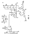
- Bias circuit 1 is adapted to provide a bias voltage to the control terminal of a power transistor 2.
- Power transistor 2 is described below and illustrated in the drawings as a radio frequency (RF) power MOS transistor which amplifies an RF input signal. It is understood that power transistor 2 may be used in conjunction with bias circuit 1 in other applications as well. It is further understood that power transistor 2 may be another type of power transistor.
- RF radio frequency
- an RF input signal is received and passes through capacitor C1 which blocks the DC signal thereof.
- Matching circuit T1 made up of one or more micro-strip lines and on zero or more capacitors and connected between capacitor C1 and power transistor 2, matches the system impedance seen at the gate terminal of power transistor 2 to the input impedance thereof.
- matching circuit T3, connected to the drain terminal of power transistor 2 matches the system impedance seen at the drain of power transistor 2 to the output impedance thereof.
- transmission line T4 which may be a quarter wave line of a relatively high impedance that is shorted at the frequency of operation by capacitor C5 and at lower frequencies by capacitors C3 and C11. Consequently, transmission line T4 has little effect over the operation of power transistor 2 at the frequency of interest while providing the Vdd reference voltage thereto.
- a low pass filter made up of ferrite beads FB1 and FB2 and capacitors C5, C8, C9 and C10, is connected between the Vdd reference and transmission line T4 and isolates power transistor 2 from the Vdd reference.
- bias circuit 1 generates a DC bias voltage level which is applied to the gate terminal of power transistor 2 so as to offset undesirable changes in the device operating characteristics thereof.
- bias circuit 1 utilizes a correction transistor 3 which is adapted to have substantially similar operating characteristics and/or device characteristics to the operating/device characteristics of power transistor 2.
- Correction transistor 3 preferably possesses the same device structure as power transistor 2.
- Power transistor 2 and correction transistor 3 may be LDMOS transistors.
- correction transistor 3 may be fabricated in the same semiconductor substrate in which power transistor 2 is fabricated.
- correction transistor 3 may be fabricated in a different semiconductor substrate from power transistor 2 using the same fabrication process in which power transistor 2 is fabricated.
- one or more dimensions of correction transistor 3 are scaled relative to the corresponding dimensions of power transistor 2.
- dimensions of correction transistor 3 are scaled to be a substantially small fraction of the size of the corresponding dimensions of power transistor 2. In this way, correction transistor 3 is capable of substantially mirroring power transistor 2 without occupying sizeable silicon space or dissipating a significant amount of power.
- Bias circuit 1 includes resistors R9 and R10 which bias the gate terminal of correction transistor 3.
- the resistance values of resistors R9 and R10 are chosen to generate a drain current for correction transistor 3 such that the ratio of the drain current of correction transistor 3 to the drain current of power transistor 2 is substantially the same as the ratio of the size of correction transistor 3 to the size of power transistor 2.
- a parallel combination of resistors R11 and R12 of bias circuit 1 preferably serves as pull-up devices for correction transistor 3. As can be seen, the drain output voltage of correction transistor 3 varies depending upon changes to the operating characteristics thereof.
- bias circuit 1 includes an operational amplifier 4.
- Operational amplifier 4 is configured as an amplifier circuit having a non-inverting closed loop gain.
- Resistors R5, R7 and R8 are connected to operational amplifier 4 and set the closed loop gain thereof.
- Resistor R5 has a first terminal connected to the non-inverting input of operational amplifier 4.
- Resistor R6 has a first terminal connected to a second terminal of resistor R5 and a second terminal connected to the ground potential.
- Resistor R7 has a first terminal connected to the inverting input of operational amplifier 4 and a second terminal connected to the output thereof.
- Capacitors C16 (connected to resistor R5) and C18 (connected in parallel with resistor R7) substantially eliminate noise induced into bias circuit 1.
- Capacitor C17 connected between the Vdd reference for operational amplifier 4 and ground, serves as a bypass capacitor for the supply voltage signal applied to operational amplifier 4.
- Resistors R1 and R6 serve as a voltage divider in setting a voltage level on the non-inverting input of operational amplifier 4.
- Bias circuit 1 further includes resistor R13 which is connected between the drain of correction transistor 3 and the second terminal of resistor R5. Providing resistor R13 between the drain of correction transistor 3 and the non-inverting input of operational amplifier 4 causes the drain voltage of correction transistor 3 to be seen at the input of operational amplifier 4.
- Series-connected resistors R3 and R4 are coupled at one end to the output of operational amplifier 4.
- Resistors R2, R3 and R4 form a voltage divider to reduce the voltage from the output of operational amplifier 4 to the desired level.
- Inductor L1 and transmission circuit T2 connected between resistor R3 and the input of transmission circuit T1, provide a low impedance DC path to power transistor 2 and a substantially high impedance path at the frequency of operation in order to block the RF input signal.
- Capacitor C4 is connected to resistor R3 to short any residual RF signaling which may appear at resistor R3.
- bias circuit 1 One benefit of bias circuit 1 according to the preferred embodiment of the present invention described above is that because operational amplifier 4 has a relatively high input impedance, there is a much broader choice of resistance values for resistors R6, R11, R12 and R13.
- bias circuit 1 is capable of providing a bias signal to the gate terminal of power transistor 2 that offsets or compensates for variations in the operating characteristics of power transistor 2 caused by the operating temperature of power transistor 2.
- Bias circuit 1 may further include a regulator circuit 5 which receives the Vdd supply and provides a regulated reference voltage level that is used to power operational amplifier 4.
- a change in the operating characteristics of power transistor 2 similarly occurs in the operating characteristics of correction transistor 3.
- the change includes an upward shift in the threshold voltage of power transistor 2 and correction transistor 3 due to the trapping of charges in the gate oxide region of power transistor 2 and correction transistor 3, respectively, the drain current in both power transistor 2 and correction transistor 3 will decrease proportionally.
- the decrease in the drain current of correction transistor 3 results in an increase in the drain voltage thereof, which increases the voltage appearing on the non-inverting input of operational amplifier 4.
- the output of operational amplifier 4 thereby increases, which increases the DC voltage appearing on the gate terminal of power transistor 2.
- the increased gate voltage causes an increase in the drain current of power transistor 2.
- the increase in the gate voltage is based upon the change in the operating characteristics of power transistor 2 and correction transistor 3, the change in operating characteristics (drain current decrease) of power transistor 2 is offset or compensated by a substantially equal amount (drain current increase) such that the operating characteristics of power transistor 2 are maintained at the desired levels.
- resistor R1 which provided a primary bias voltage to operational amplifier 4 in bias circuit 1
- Capacitors C14 and C15 which are connected to the gate and drain terminals of correction transistor 3, respectively, quell stray RF amplification in correction transistor 3.
- Parallel-connected pull-up resistors R11 and R12 connect the drain terminal of correction transistor 3 to the Vdd reference.
- the drain voltage of correction transistor 3 is provided to the primary bias circuitry of power transistor 2 through resistor R4.
- Correction transistor 3 is sized and dimensioned relative to power transistor 2 so as to be a scaled version thereof.
- the gate terminal of correction transistor 3 in bias circuit 10 is biased by resistors R9 and R10 so that the ratio of the drain current of correction transistor 3 to the drain current of power transistor 2 is substantially the same as the ratio of the size of correction transistor 3 to the size of power transistor 2.
- the output (drain) voltage of correction transistor 3 provides an offset or correction voltage that accounts for unwanted variations in the operating performance of correction transistor 3 and power transistor 2.
- This offset or correction voltage is added to the primary bias voltage generated by resistor R1 and the resulting bias voltage is applied to the gate terminal of power transistor 2. Consequently, the resulting bias voltage appearing on the gate terminal of power transistor 2 corrects for unwanted variation in the operating performance of power transistor 2 so that power transistor 2 performs as desired.
Landscapes
- Engineering & Computer Science (AREA)
- Power Engineering (AREA)
- Amplifiers (AREA)
- Microwave Amplifiers (AREA)
Claims (27)
- Vorspannungsschaltkreis (1, 10) für einen Leistungstransistor (2), der nachfolgendes umfasst:einen Korrekturtransistor (3), der eine Bauelementeigenschaft aufweist, die im Wesentlichen die Gleiche ist wie die Bauelementeigenschaft des Leistungstransistors (2);ein den besagten Korrekturtransistor (3) umfassenden Vorspannungsschaltkreis für den Vorspannungsbetrieb eines Steuerungsanschlusselements des Korrekturtransistors (3), wobei die Betriebskennlinien des Korrekturtransistors (3) den Betriebskennlinien des Leistungstransistors (2) im Wesentlichen ähnlich sind, ein Ausgangsanschlusselement des Korrekturtransistors (3) mit dem Steuerungsanschlusselement des Leistungstransistors (2) verbunden ist, so dass ein an das Steuerungsanschlusselement des Leistungstransistors (2) angelegtes Signal von dem Ausgangsanschlusselement des Korrekturtransistors (3) die Veränderungen in den Betriebskennlinien des Leistungstransistors (2) kompensiert, gekennzeichnet durch:eine Verstärkerschaltung (4), die ein mit dem Ausgangsanschlusselement des Korrekturtransistors (3) verbundenes Verstärkereingangsanschlusselement aufweist und wobei die Verstärkerschaltung (4) weiterhin ein mit dem Steuerungsanschlusselement des Leistungstransistors (2) verbundenes Verstärkerausgangsanschlusselement aufweist; undwobei mindestens eine Abmessung und mindestens ein Strompegel des Korrekturtransistors (3) relativ skaliert sind zu einer jeweils entsprechenden mindestens einen Abmessung und einem jeweils entsprechenden mindestens einen Strompegel des Leistungstransistors (2).
- Vorspannungsschaltkreis nach Anspruch 1, wobei:der Leistungstransistor und der Korrekturtransistor MOS Transistoren sind.
- Vorspannungsschaltkreis nach Anspruch 1, wobei:der Leistungstransistor und der Korrekturtransistor LDMOS Transistoren sind.
- Vorspannungsschaltkreis nach Anspruch 1, wobei:der Korrekturtransistor (3) und der Leistungstransistor (2) MOS Transistoren umfassen; undÄnderungen in den Betriebskennlinien des Korrekturtransistors auf Grund von Aufladung des Gateoxids in dem Signal wiedergegeben werden, das an dem Steuerungsanschlusselement des Leistungstransistors anliegt, um so Veränderungen in den Betriebskennlinien des Leistungstransistors auf Grund von Aufladung des Gateoxids auszugleichen.
- Vorspannungsschaltkreis nach Anspruch 4, der weiterhin nachfolgendes umfasst:einen Spannungsteiler (R2, R3, R4), der zwischen dem Ausgang der Verstärkerschaltung und dem Steuerungsanschlusselement des Leistungstransistors geschaltet ist.
- Vorspannungsschaltkreis nach Anspruch 5, der weiterhin nachfolgendes umfasst:eine zwischen dem elektrischen Spannungsteiler und dem Steuerungsanschlusselement des Leistungstransistors geschaltete Tiefpassfilterschaltung (FB1, FB2, C5, C8, C9, C10).
- Vorspannungsschaltkreis nach Anspruch 1, der weiterhin nachfolgendes umfasst:mindestens eine zwischen einem Drain-Anschlusselement des Korrekturtransistors (3) und einer Spannungsreferenz geschaltete pull-up Anordnung (R11, R12).
- Vorspannungsschaltkreis nach Anspruch 1, wobei:eine oder mehrere Abmessungen des Korrekturtransistors (3) relativ zu entsprechenden Abmessungen des Leistungstransistors (2) skaliert sind.
- Vorspannungsschaltkreis nach Anspruch 8, wobei:das Verhältnis des Strompegels des Korrekturtransistors (3) zum Strompegel des Leistungstransistors (2) im Wesentlichen das Gleiche ist wie das Verhältnis der Abmessungen des Korrekturtransistors (3) zu den entsprechenden Abmessungen des Leistungstransistors (2).
- Vorspannungsschaltkreis nach Anspruch 1, wobei:der Leistungstransistor (2) ein HF Eingangssignal an seinem Steuerungsanschlusselement empfängt und ein HF Ausgangssignal erzeugt.
- Vorspannungsschaltkreis nach Anspruch 10, wobei:ein Drain-Anschlusselement des Leistungstransistors (2) mit einer Referenzspannung verbunden ist.
- Vorspannungsschaltkreis nach Anspruch 1, der weiterhin nachfolgendes umfasst:einen zwischen einem Ausgangsanschlusselement des Korrekturtransistors und dem Steuerungsanschlusselement des Leistungstransistors geschalteten Spannungsteiler.
- Vorspannungsschaltkreis nach Anspruch 1, der weiterhin nachfolgendes umfasst:einen Operationsverstärker (4), der einen mit dem Ausgangsanschlusselement des Korrekturtransistors (3) verbundenen Eingang und einen mit dem Steuerungsanschlusselement des Leistungstransistors (2) verbundenen Ausgang aufweist.
- Verfahren zur Beaufschlagung eines Leistungstransistors (2) mit einer Vorspannung, gekennzeichnet durch die Schritte:im Wesentlichen Widerspiegeln der Betriebskennlinien des Leistungstransistors (2) in einem Korrekturtransistor (3);Erzeugen eines Vorspannungssignals basierend auf den übereinstimmenden Betriebskennlinien; undVerbinden des Vorspannungssignals mit dem Steuerungsanschlusselement des Leistungstransistors (2), um eine Veränderung in der Betriebskennlinie des Leistungstransistors (2) zu kompensieren, wobei:der Schritt des Widerspiegelns den Schritt umfasst, ein elektrisches Signal zu erzeugen, welches im Wesentlichen mit einem Strompegel des Leistungstransistors (2) übereinstimmt;der Schritt ein Vorspannungssignal zu erzeugen den Schritt umfasst, das elektrische Signal zu verstärken, um ein verstärktes elektrisches Signal zu erzeugen; und der Schritt des Verbindens den Schritt umfasst, das verstärkte elektrische Signal mit dem Steuerungsanschlusselement des Leistungstransistors (2) zu verbinden.
- Verfahren nach Anspruch 14, wobei der Korrekturtransistor (3) und der Leistungstransistor (2) MOS Transistoren umfassen.
- Verfahren nach Anspruch 15, wobei:der Schritt, ein Vorspannungssignal zu erzeugen, den Schritt umfasst, das verstärkte elektrische Signal zu teilen, um ein geteiltes Signal zu erhalten; undder Schritt des Verbindens den Schritt umfasst, das geteilte Signal mit dem Steuerungsanschlusselement des Leistungstransistors zu verbinden.
- Verfahren nach Anspruch 15, wobei:der Schritt, ein elektrisches Signal zu erzeugen, weiterhin den Schritt umfasst, das elektrische Signal zu skalieren.
- Verfahren nach Anspruch 14, wobei:der Schritt des Widerspiegelns den Schritt umfasst, eine Veränderung der Schwellenspannung des Leistungstransistors (2) anzupassen; undder Schritt, ein Vorspannungssignal zu erzeugen, das Vorspannungssignal erzeugt, um die Veränderung der Schwellenspannung des Leistungstransistors (2) auszugleichen.
- Verstärkerschaltung die nachfolgendes umfasst:einen ersten Transistor (2), der ein Steuerungsanschlusselement aufweist, das verbunden ist, um ein Hochfrequenzeingangssignal zu empfangen, und ein Ausgangsanschlusselement aufweist, das ein Hochfrequenzausgangssignal zur Verfügung stellt, das auf dem Hochfrequenzeingangssignal basiert;eine pull-up Anordnung, die mit dem Ausgangsanschlusselement des ersten Transistors (2) verbunden ist; undeinen Vorspannungsschaltkreis (1, 10), der mit dem Steuerungsanschlusselement des ersten Transistors (2) verbunden ist, zur Erzeugung eines Vorspannungssignals, das den ersten Transistor (2) mit einer Vorspannung beaufschlagt, um das Hochfrequenzeingangssignal zu verstärken, wobei der Vorspannungsschaltkreis (1, 10) einen Korrekturtransistor (3) umfasst, der Betriebskennlinien aufweist, welche im Wesentlichen mit den Betriebskennlinien des ersten Transistor (2) übereinstimmen, wobei das Vorspannungssignal von den Betriebskennlinien des Korrekturtransistors (3) abhängt, um die Änderung in den Betriebskennlinien des ersten Transistor (2) zu kompensieren; dadurch gekennzeichnet, dass:die Betriebskennlinien des Korrekturtransistors (3) im Wesentlichen mindestens zum Teil mit den Betriebskennlinien des ersten Transistors (2) übereinstimmen als Ergebnis dessen, dass mindestens eine Abmessung des Korrekturtransistors (3) relativ zu einer entsprechenden mindestens einen Abmessung des ersten Transistors (2) skaliert ist, undder Vorspannungsschaltkreis (1, 10) weiterhin einen Verstärker (4) umfasst, der einen Verstärkereingang aufweist, der mit einem Ausgangsanschlusselement des Korrekturtransistors (3) verbunden ist und der Verstärkers (4) weiterhin einen Verstärkerausgang aufweist, der mit dem Steuerungsanschlusselement des ersten Transistors (2) verbunden ist.
- Verstärkerschaltung nach Anspruch 19, wobei:die Bauelementstruktur des Korrekturtransistors im Wesentlichen die Gleiche ist wie die Bauelementstruktur des ersten Transistors.
- Verstärkerschaltung nach Anspruch 20, wobei:mindestens eine Abmessung des Korrekturtransistors relativ zu der entsprechenden Abmessung des ersten Transistors skaliert ist.
- Verstärkerschaltung nach Anspruch 19, wobei:der Verstärker (4) einen Operationsverstärker (4) umfasst.
- Verstärkerschaltung nach Anspruch 22, wobei:der Operationsverstärker (4) eine nicht invertierende Kreisverstärkung aufweist.
- Verstärkerschaltung nach Anspruch 19, wobei:der Korrekturtransistor und der erste Transistor MOS Transistoren sind.
- Verstärkerschaltung nach Anspruch 24, wobei:der Korrekturtransistor und der erste Transistor LDMOS Transistoren sind.
- Verstärkerschaltung nach Anspruch 24, wobei:Änderungen in den Betriebskennlinien des Korrekturtransistors auf Grund von Aufladung des Gateoxids in dem von dem Vorspannungsschaltkreis erzeugten Vorspannungssignal widergespiegelt werden, um Änderungen in den Betriebskennlinien des ersten Transistors auf Grund von Aufladung des Gateoxids auszugleichen.
- Verstärkerschaltung nach Anspruch 19, wobei:der erste Transistor und der Korrekturtransistor im Wesentlichen dieselben Temperaturkennlinien aufweisen; undÄnderungen in den Betriebskennlinien des Korrekturtransistors auf Grund der Temperatur in dem von dem Vorspannungsschaltkreis erzeugten Vorspannungssignal widergespiegelt werden, um Änderungen in den Betriebskennlinien des ersten Transistors auf Grund der Temperatur auszugleichen.
Applications Claiming Priority (3)
| Application Number | Priority Date | Filing Date | Title |
|---|---|---|---|
| US415524 | 1999-10-08 | ||
| US09/415,524 US6304129B1 (en) | 1999-10-08 | 1999-10-08 | Compensation circuit and method for a power transistor |
| PCT/US2000/027199 WO2001028086A1 (en) | 1999-10-08 | 2000-10-03 | Compensation circuit and method for a power transistor |
Publications (2)
| Publication Number | Publication Date |
|---|---|
| EP1224732A1 EP1224732A1 (de) | 2002-07-24 |
| EP1224732B1 true EP1224732B1 (de) | 2006-10-25 |
Family
ID=23646044
Family Applications (1)
| Application Number | Title | Priority Date | Filing Date |
|---|---|---|---|
| EP00967260A Expired - Lifetime EP1224732B1 (de) | 1999-10-08 | 2000-10-03 | Kompensationsschaltung und verfahren für einen leistungstransistor |
Country Status (9)
| Country | Link |
|---|---|
| US (1) | US6304129B1 (de) |
| EP (1) | EP1224732B1 (de) |
| JP (1) | JP2003511945A (de) |
| CN (1) | CN1258870C (de) |
| AT (1) | ATE343868T1 (de) |
| AU (1) | AU7748400A (de) |
| DE (1) | DE60031561T2 (de) |
| TW (1) | TW478244B (de) |
| WO (1) | WO2001028086A1 (de) |
Families Citing this family (11)
| Publication number | Priority date | Publication date | Assignee | Title |
|---|---|---|---|---|
| GB0103082D0 (en) * | 2001-02-08 | 2001-03-28 | Pace Micro Tech Plc | Self compensating amplifier and driver |
| US6893101B2 (en) | 2001-07-27 | 2005-05-17 | Telefonaktiebolaget L.M. Ericsson | Active element bias circuit for RF power transistor input |
| JP4075505B2 (ja) * | 2001-09-10 | 2008-04-16 | セイコーエプソン株式会社 | 電子回路、電子装置、及び電子機器 |
| US7422366B1 (en) * | 2004-09-10 | 2008-09-09 | National Semiconductor Corporation | Current mirror methodology quantifying time dependent thermal instability accurately in SOI BJT circuitry |
| JP2006311507A (ja) * | 2005-03-28 | 2006-11-09 | Matsushita Electric Ind Co Ltd | 電源スイッチ回路 |
| US7724084B2 (en) | 2007-01-25 | 2010-05-25 | Research In Motion Limited | System and method for controlling radio frequency transmissions from an electronic device |
| EP2161835B1 (de) * | 2007-01-25 | 2013-08-14 | Research In Motion Limited | System und Verfahren zur Filterung von Harmonischen eines Leistungsverstärkers |
| US9041369B2 (en) * | 2012-08-24 | 2015-05-26 | Sandisk Technologies Inc. | Method and apparatus for optimizing linear regulator transient performance |
| CN103957009B (zh) * | 2014-04-29 | 2017-01-25 | 电子科技大学 | 一种对压缩采样系统低通滤波器进行补偿的方法 |
| KR101977783B1 (ko) * | 2017-10-17 | 2019-05-13 | 주식회사 케이엠더블유 | 전력 증폭기 성능 보정 방법 및 그를 위한 장치 |
| US12374991B2 (en) * | 2022-09-01 | 2025-07-29 | Navitas Semiconductor Limited | Systems and methods for improving radiated EMI in switching power supplies |
Family Cites Families (7)
| Publication number | Priority date | Publication date | Assignee | Title |
|---|---|---|---|---|
| US5214315A (en) * | 1991-04-23 | 1993-05-25 | Cornell Research Foundation, Inc. | Nanosecond RF switch driver |
| US5164679A (en) | 1992-01-08 | 1992-11-17 | Harris Corporation | AC power amplifier having current limit control |
| US5281925A (en) * | 1992-11-17 | 1994-01-25 | Acrodyne Industries, Inc. | RF amplifier providing reduced drive response rise times and fall times |
| JP3365428B2 (ja) | 1992-12-09 | 2003-01-14 | ソニー株式会社 | 高周波パワーアンプのバイアス制御回路 |
| JPH06334445A (ja) | 1993-05-19 | 1994-12-02 | Mitsubishi Electric Corp | 半導体集積回路 |
| US6049704A (en) * | 1997-12-10 | 2000-04-11 | Motorola, Inc. | Apparatus for amplifying an RF signal |
| US6091279A (en) * | 1998-04-13 | 2000-07-18 | Lucent Technologies, Inc. | Temperature compensation of LDMOS devices |
-
1999
- 1999-10-08 US US09/415,524 patent/US6304129B1/en not_active Expired - Fee Related
-
2000
- 2000-10-03 CN CNB008169071A patent/CN1258870C/zh not_active Expired - Fee Related
- 2000-10-03 DE DE60031561T patent/DE60031561T2/de not_active Expired - Fee Related
- 2000-10-03 WO PCT/US2000/027199 patent/WO2001028086A1/en not_active Ceased
- 2000-10-03 JP JP2001530195A patent/JP2003511945A/ja active Pending
- 2000-10-03 AU AU77484/00A patent/AU7748400A/en not_active Abandoned
- 2000-10-03 AT AT00967260T patent/ATE343868T1/de not_active IP Right Cessation
- 2000-10-03 EP EP00967260A patent/EP1224732B1/de not_active Expired - Lifetime
- 2000-11-01 TW TW089120775A patent/TW478244B/zh not_active IP Right Cessation
Also Published As
| Publication number | Publication date |
|---|---|
| CN1409893A (zh) | 2003-04-09 |
| EP1224732A1 (de) | 2002-07-24 |
| AU7748400A (en) | 2001-04-23 |
| TW478244B (en) | 2002-03-01 |
| DE60031561T2 (de) | 2007-09-13 |
| WO2001028086A1 (en) | 2001-04-19 |
| JP2003511945A (ja) | 2003-03-25 |
| CN1258870C (zh) | 2006-06-07 |
| US6304129B1 (en) | 2001-10-16 |
| ATE343868T1 (de) | 2006-11-15 |
| DE60031561D1 (de) | 2006-12-07 |
Similar Documents
| Publication | Publication Date | Title |
|---|---|---|
| US11846660B2 (en) | Power detector with wide dynamic range | |
| EP1224732B1 (de) | Kompensationsschaltung und verfahren für einen leistungstransistor | |
| US6667657B2 (en) | RF variable gain amplifying device | |
| US7863980B2 (en) | Amplifiers with negative capacitance circuits | |
| US5387880A (en) | Compact monolithic wide band HEMT low noise amplifiers with regulated self-bias | |
| KR100861877B1 (ko) | 전자 장치를 선형화하는 회로 | |
| US6819180B2 (en) | Radio frequency power amplifier adaptive bias control circuit | |
| US20040100327A1 (en) | Radio frequency power amplifier active self-bias compensation circuit | |
| US8031002B2 (en) | Buffer amplifier | |
| US5510699A (en) | Voltage regulator | |
| US7071769B1 (en) | Frequency boosting circuit for high swing cascode | |
| KR20000037693A (ko) | 능동소자 발룬을 이용한 소신호 선형성 향상을 위한 알에프 집적회로 | |
| JP3371151B2 (ja) | モノリシックマイクロウエーブ半導体集積回路 | |
| US7368993B2 (en) | Transconductance circuit with improved linearity | |
| WO2003049280A1 (en) | A low noise electronic circuit | |
| WO2005109627A1 (en) | Amplifier bias enhancement technique | |
| US20260012138A1 (en) | Push-pull source follower circuit using biasing technique to program bias current and output mean voltage independently | |
| KR100816368B1 (ko) | 선형성 개선 씨모스 인버터 | |
| US20250300610A1 (en) | Low Noise Amplifier Circuit Capable of Enhancing Operational Linearity and Noise Reduction Performance | |
| KR100446003B1 (ko) | 차동 증폭기의 오프셋 제거 회로 및 오프셋이 억제된 차동증폭기 | |
| KR100394275B1 (ko) | 소신호 선형성 향상을 위한 알에프용 차동증폭단 회로 | |
| RU2274946C2 (ru) | Схема для линеаризации электронных устройств | |
| CN117478077A (zh) | 具有伪ab类结构的电路 |
Legal Events
| Date | Code | Title | Description |
|---|---|---|---|
| PUAI | Public reference made under article 153(3) epc to a published international application that has entered the european phase |
Free format text: ORIGINAL CODE: 0009012 |
|
| 17P | Request for examination filed |
Effective date: 20020426 |
|
| AK | Designated contracting states |
Kind code of ref document: A1 Designated state(s): AT BE CH CY DE DK ES FI FR GB GR IE IT LI LU MC NL PT SE |
|
| AX | Request for extension of the european patent |
Free format text: AL;LT;LV;MK;RO;SI |
|
| RAP1 | Party data changed (applicant data changed or rights of an application transferred) |
Owner name: INFINEON TECHNOLOGIES AG |
|
| GRAP | Despatch of communication of intention to grant a patent |
Free format text: ORIGINAL CODE: EPIDOSNIGR1 |
|
| GRAS | Grant fee paid |
Free format text: ORIGINAL CODE: EPIDOSNIGR3 |
|
| GRAA | (expected) grant |
Free format text: ORIGINAL CODE: 0009210 |
|
| AK | Designated contracting states |
Kind code of ref document: B1 Designated state(s): AT BE CH CY DE DK ES FI FR GB GR IE IT LI LU MC NL PT SE |
|
| PG25 | Lapsed in a contracting state [announced via postgrant information from national office to epo] |
Ref country code: IT Free format text: LAPSE BECAUSE OF FAILURE TO SUBMIT A TRANSLATION OF THE DESCRIPTION OR TO PAY THE FEE WITHIN THE PRESCRIBED TIME-LIMIT;WARNING: LAPSES OF ITALIAN PATENTS WITH EFFECTIVE DATE BEFORE 2007 MAY HAVE OCCURRED AT ANY TIME BEFORE 2007. THE CORRECT EFFECTIVE DATE MAY BE DIFFERENT FROM THE ONE RECORDED. Effective date: 20061025 Ref country code: NL Free format text: LAPSE BECAUSE OF FAILURE TO SUBMIT A TRANSLATION OF THE DESCRIPTION OR TO PAY THE FEE WITHIN THE PRESCRIBED TIME-LIMIT Effective date: 20061025 Ref country code: LI Free format text: LAPSE BECAUSE OF FAILURE TO SUBMIT A TRANSLATION OF THE DESCRIPTION OR TO PAY THE FEE WITHIN THE PRESCRIBED TIME-LIMIT Effective date: 20061025 Ref country code: BE Free format text: LAPSE BECAUSE OF FAILURE TO SUBMIT A TRANSLATION OF THE DESCRIPTION OR TO PAY THE FEE WITHIN THE PRESCRIBED TIME-LIMIT Effective date: 20061025 Ref country code: AT Free format text: LAPSE BECAUSE OF FAILURE TO SUBMIT A TRANSLATION OF THE DESCRIPTION OR TO PAY THE FEE WITHIN THE PRESCRIBED TIME-LIMIT Effective date: 20061025 Ref country code: FI Free format text: LAPSE BECAUSE OF FAILURE TO SUBMIT A TRANSLATION OF THE DESCRIPTION OR TO PAY THE FEE WITHIN THE PRESCRIBED TIME-LIMIT Effective date: 20061025 Ref country code: CH Free format text: LAPSE BECAUSE OF FAILURE TO SUBMIT A TRANSLATION OF THE DESCRIPTION OR TO PAY THE FEE WITHIN THE PRESCRIBED TIME-LIMIT Effective date: 20061025 |
|
| REG | Reference to a national code |
Ref country code: GB Ref legal event code: FG4D |
|
| REG | Reference to a national code |
Ref country code: CH Ref legal event code: EP |
|
| REG | Reference to a national code |
Ref country code: IE Ref legal event code: FG4D |
|
| REF | Corresponds to: |
Ref document number: 60031561 Country of ref document: DE Date of ref document: 20061207 Kind code of ref document: P |
|
| PG25 | Lapsed in a contracting state [announced via postgrant information from national office to epo] |
Ref country code: SE Free format text: LAPSE BECAUSE OF FAILURE TO SUBMIT A TRANSLATION OF THE DESCRIPTION OR TO PAY THE FEE WITHIN THE PRESCRIBED TIME-LIMIT Effective date: 20070125 Ref country code: DK Free format text: LAPSE BECAUSE OF FAILURE TO SUBMIT A TRANSLATION OF THE DESCRIPTION OR TO PAY THE FEE WITHIN THE PRESCRIBED TIME-LIMIT Effective date: 20070125 |
|
| PG25 | Lapsed in a contracting state [announced via postgrant information from national office to epo] |
Ref country code: ES Free format text: LAPSE BECAUSE OF FAILURE TO SUBMIT A TRANSLATION OF THE DESCRIPTION OR TO PAY THE FEE WITHIN THE PRESCRIBED TIME-LIMIT Effective date: 20070205 |
|
| PG25 | Lapsed in a contracting state [announced via postgrant information from national office to epo] |
Ref country code: PT Free format text: LAPSE BECAUSE OF FAILURE TO SUBMIT A TRANSLATION OF THE DESCRIPTION OR TO PAY THE FEE WITHIN THE PRESCRIBED TIME-LIMIT Effective date: 20070326 |
|
| NLV1 | Nl: lapsed or annulled due to failure to fulfill the requirements of art. 29p and 29m of the patents act | ||
| REG | Reference to a national code |
Ref country code: CH Ref legal event code: PL |
|
| EN | Fr: translation not filed | ||
| PLBE | No opposition filed within time limit |
Free format text: ORIGINAL CODE: 0009261 |
|
| STAA | Information on the status of an ep patent application or granted ep patent |
Free format text: STATUS: NO OPPOSITION FILED WITHIN TIME LIMIT |
|
| 26N | No opposition filed |
Effective date: 20070726 |
|
| PG25 | Lapsed in a contracting state [announced via postgrant information from national office to epo] |
Ref country code: FR Free format text: LAPSE BECAUSE OF FAILURE TO SUBMIT A TRANSLATION OF THE DESCRIPTION OR TO PAY THE FEE WITHIN THE PRESCRIBED TIME-LIMIT Effective date: 20070608 Ref country code: GR Free format text: LAPSE BECAUSE OF FAILURE TO SUBMIT A TRANSLATION OF THE DESCRIPTION OR TO PAY THE FEE WITHIN THE PRESCRIBED TIME-LIMIT Effective date: 20070126 |
|
| PG25 | Lapsed in a contracting state [announced via postgrant information from national office to epo] |
Ref country code: MC Free format text: LAPSE BECAUSE OF NON-PAYMENT OF DUE FEES Effective date: 20071031 |
|
| GBPC | Gb: european patent ceased through non-payment of renewal fee |
Effective date: 20071003 |
|
| PG25 | Lapsed in a contracting state [announced via postgrant information from national office to epo] |
Ref country code: DE Free format text: LAPSE BECAUSE OF NON-PAYMENT OF DUE FEES Effective date: 20080501 |
|
| PG25 | Lapsed in a contracting state [announced via postgrant information from national office to epo] |
Ref country code: IE Free format text: LAPSE BECAUSE OF NON-PAYMENT OF DUE FEES Effective date: 20071003 |
|
| PG25 | Lapsed in a contracting state [announced via postgrant information from national office to epo] |
Ref country code: GB Free format text: LAPSE BECAUSE OF NON-PAYMENT OF DUE FEES Effective date: 20071003 Ref country code: FR Free format text: LAPSE BECAUSE OF FAILURE TO SUBMIT A TRANSLATION OF THE DESCRIPTION OR TO PAY THE FEE WITHIN THE PRESCRIBED TIME-LIMIT Effective date: 20061025 |
|
| PG25 | Lapsed in a contracting state [announced via postgrant information from national office to epo] |
Ref country code: CY Free format text: LAPSE BECAUSE OF FAILURE TO SUBMIT A TRANSLATION OF THE DESCRIPTION OR TO PAY THE FEE WITHIN THE PRESCRIBED TIME-LIMIT Effective date: 20061025 Ref country code: LU Free format text: LAPSE BECAUSE OF NON-PAYMENT OF DUE FEES Effective date: 20071003 |