EP1225623A2 - Ein Verfahren zur Herstellung von auf einem Grabenwand begrabene Source und Drain mittels einen Austauschgatter-Technik - Google Patents
Ein Verfahren zur Herstellung von auf einem Grabenwand begrabene Source und Drain mittels einen Austauschgatter-Technik Download PDFInfo
- Publication number
- EP1225623A2 EP1225623A2 EP02368006A EP02368006A EP1225623A2 EP 1225623 A2 EP1225623 A2 EP 1225623A2 EP 02368006 A EP02368006 A EP 02368006A EP 02368006 A EP02368006 A EP 02368006A EP 1225623 A2 EP1225623 A2 EP 1225623A2
- Authority
- EP
- European Patent Office
- Prior art keywords
- conductive material
- dielectric layer
- substrate
- shallow trench
- forming
- Prior art date
- Legal status (The legal status is an assumption and is not a legal conclusion. Google has not performed a legal analysis and makes no representation as to the accuracy of the status listed.)
- Withdrawn
Links
Images


Classifications
-
- H—ELECTRICITY
- H10—SEMICONDUCTOR DEVICES; ELECTRIC SOLID-STATE DEVICES NOT OTHERWISE PROVIDED FOR
- H10D—INORGANIC ELECTRIC SEMICONDUCTOR DEVICES
- H10D30/00—Field-effect transistors [FET]
- H10D30/01—Manufacture or treatment
- H10D30/021—Manufacture or treatment of FETs having insulated gates [IGFET]
- H10D30/0223—Manufacture or treatment of FETs having insulated gates [IGFET] having source and drain regions or source and drain extensions self-aligned to sides of the gate
- H10D30/0225—Manufacture or treatment of FETs having insulated gates [IGFET] having source and drain regions or source and drain extensions self-aligned to sides of the gate using an initial gate mask complementary to the prospective gate location, e.g. using dummy source and drain electrodes
-
- H—ELECTRICITY
- H10—SEMICONDUCTOR DEVICES; ELECTRIC SOLID-STATE DEVICES NOT OTHERWISE PROVIDED FOR
- H10D—INORGANIC ELECTRIC SEMICONDUCTOR DEVICES
- H10D62/00—Semiconductor bodies, or regions thereof, of devices having potential barriers
- H10D62/01—Manufacture or treatment
- H10D62/021—Forming source or drain recesses by etching e.g. recessing by etching and then refilling
-
- H—ELECTRICITY
- H10—SEMICONDUCTOR DEVICES; ELECTRIC SOLID-STATE DEVICES NOT OTHERWISE PROVIDED FOR
- H10D—INORGANIC ELECTRIC SEMICONDUCTOR DEVICES
- H10D64/00—Electrodes of devices having potential barriers
- H10D64/01—Manufacture or treatment
- H10D64/018—Spacers formed inside holes at the prospective gate locations, e.g. holes left by removing dummy gates
-
- H—ELECTRICITY
- H10—SEMICONDUCTOR DEVICES; ELECTRIC SOLID-STATE DEVICES NOT OTHERWISE PROVIDED FOR
- H10D—INORGANIC ELECTRIC SEMICONDUCTOR DEVICES
- H10D64/00—Electrodes of devices having potential barriers
- H10D64/20—Electrodes characterised by their shapes, relative sizes or dispositions
- H10D64/23—Electrodes carrying the current to be rectified, amplified, oscillated or switched, e.g. sources, drains, anodes or cathodes
- H10D64/251—Source or drain electrodes for field-effect devices
- H10D64/258—Source or drain electrodes for field-effect devices characterised by the relative positions of the source or drain electrodes with respect to the gate electrode
- H10D64/259—Source or drain electrodes being self-aligned with the gate electrode and having bottom surfaces higher than the interface between the channel and the gate dielectric
-
- H—ELECTRICITY
- H10—SEMICONDUCTOR DEVICES; ELECTRIC SOLID-STATE DEVICES NOT OTHERWISE PROVIDED FOR
- H10D—INORGANIC ELECTRIC SEMICONDUCTOR DEVICES
- H10D64/00—Electrodes of devices having potential barriers
- H10D64/60—Electrodes characterised by their materials
- H10D64/66—Electrodes having a conductor capacitively coupled to a semiconductor by an insulator, e.g. MIS electrodes
- H10D64/671—Electrodes having a conductor capacitively coupled to a semiconductor by an insulator, e.g. MIS electrodes the conductor having lateral variation in doping or structure
-
- H—ELECTRICITY
- H10—SEMICONDUCTOR DEVICES; ELECTRIC SOLID-STATE DEVICES NOT OTHERWISE PROVIDED FOR
- H10D—INORGANIC ELECTRIC SEMICONDUCTOR DEVICES
- H10D64/00—Electrodes of devices having potential barriers
- H10D64/01—Manufacture or treatment
- H10D64/021—Manufacture or treatment using multiple gate spacer layers, e.g. bilayered sidewall spacers
-
- H—ELECTRICITY
- H10—SEMICONDUCTOR DEVICES; ELECTRIC SOLID-STATE DEVICES NOT OTHERWISE PROVIDED FOR
- H10W—GENERIC PACKAGES, INTERCONNECTIONS, CONNECTORS OR OTHER CONSTRUCTIONAL DETAILS OF DEVICES COVERED BY CLASS H10
- H10W10/00—Isolation regions in semiconductor bodies between components of integrated devices
- H10W10/01—Manufacture or treatment
- H10W10/011—Manufacture or treatment of isolation regions comprising dielectric materials
- H10W10/014—Manufacture or treatment of isolation regions comprising dielectric materials using trench refilling with dielectric materials, e.g. shallow trench isolations
-
- H—ELECTRICITY
- H10—SEMICONDUCTOR DEVICES; ELECTRIC SOLID-STATE DEVICES NOT OTHERWISE PROVIDED FOR
- H10W—GENERIC PACKAGES, INTERCONNECTIONS, CONNECTORS OR OTHER CONSTRUCTIONAL DETAILS OF DEVICES COVERED BY CLASS H10
- H10W10/00—Isolation regions in semiconductor bodies between components of integrated devices
- H10W10/10—Isolation regions comprising dielectric materials
- H10W10/17—Isolation regions comprising dielectric materials formed using trench refilling with dielectric materials, e.g. shallow trench isolations
Definitions
- the present invention relates generally to semiconductor devices and to an improved MOS transistor and the method of making an MOS transistor. More particularly, the present invention relates to a method to form a recessed source drain on a trench sidewall with a replacement gate technique.
- MOS transistors are well known in the art, however there are some structures of MOS transistors that show problems.
- High junction capacitance degrades speed and performance of a transistor. This high junction capacitance can be reduced by the sitting source drain on top of the shallow trench isolation of a transistor.
- High junction leakages produce size problems so that the transistor has to be made bigger then ideal. This high junction leakage can be reduced when only the lightly doped drain is on top of a substrate.
- scaling of the active area effects the overall package density of a transistor and a vertical active contact, results in a better smaller package of a transistor.
- U.S. Pat. No. 5,795,811 discloses a shallow trench isolation process, but does not disclose the source drain sitting on top of the shallow trench isolation.
- U.S. Pat. No. 5,380,671 shows a buried contact method near the shallow trench isolations.
- U.S. Pat. No.5, 643,822 teaches an ion implant into the shallow trench isolations silicon trench sidewalls.
- U.S. Pat. No. 5,879,998 shows a replacement gate process.
- the present invention provides an improved MOS transistor and method of making an improved MOS transistor.
- Another purpose of the present invention is to provide an MOS transistor having a recessed source drain on a trench sidewall with a replacement gate technique.
- MOS transistors are well known in the art, and it is well known in the art that they can be either an N-MOS transistor or a P-MOS transistor. In this application we will show an N-MOS transistor, but as well known in the art, one can easily apply these descriptions to a P-MOS transistor.
- a method for forming an MOS transistor by first providing a substrate and forming a pad oxide over the substrate. Then forming an etch stop layer over the pad oxide and creating shallow trench isolations in the substrate pad oxide, and etch stop layers. Active areas of the substrate are located between the shallow trench isolations. Next holes are formed in the shallow trench isolations, which exposes sidewall of the substrate in the active area. Sidewalls of the substrate are doped in the active area where holes are. Conductive material is then formed in the holes and the conductive material becomes the source and drain regions.
- the etch stop layer is then removed exposing sidewalls of the conductive material, and oxidizing exposed sidewalls of the conductive material is preformed. Spacers are formed on top of the pad oxide and on the sidewalls of the oxidized portions of the conductive material.
- the pad oxide layer is removed from the structure but not from under the spacers.
- a gate dielectric layer is formed on the substrate in the active area between the spacers; and a gate electrode is formed on said gate dielectric layer.
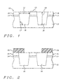
- a basic structure 10 is a standard MOS structure made by standard shallow trench isolation process.
- the shallow trench process consists of forming a trench through a pad dielectric layer, an etch stop layer and in the substrate. Filling the trench formed with a dielectric material, which forms shallow trench isolations. Finally, the dielectric material that fills the trench is then post chemical mechanically polished.
- Basic structure 10 has a substrate 12, with a pad dielectric layer 14 on the substrate 12.
- the pad dielectric layer 14 is preferably made of silicon oxide.
- the pad dielectric layer 14 has a thickness of about 100 to 200 Angstroms but preferably 150 Angstroms.
- An etch stop 16 is formed on the pad dielectric layer 14. The etch stop 16 is preferably silicon nitride.
- the etch stop 16 has a thickness of about 1000 to 2000 angstroms but preferably 1500 angstroms.
- the substrate, etch stop and pad dielectric layer having shallow trench isolations 18 located therein.
- the shallow trench isolations are usually made of silicon oxide.
- the shallow trench isolations 18 define active areas 13, which are areas of the substrate between the shallow trench isolations (STI).
- the dimensions of the shallow trench isolations 18 is a diameter at the top 11 of about .1 to .3 um and a depth 15 of .2 to .4 um.
- An angle 17 between the sidewall of the shallow isolation trench and the bottom of the shallow isolation trench is between 75 to 88 degrees. Therefore, the diameter at the bottom of the isolation trench would depend on the diameter at the top and the depth.
- the active area 13 is the distance between the two shallow isolation trenches 18 and is about .1 to .3 um.
- a photo-resist 19 is then placed on the structure to pattern the shallow trench isolations using etching that affects only the oxide.
- the shallow trench isolation 18 is etched using the photoresist 19 as a etch mask.
- the etching forms a hole or pattern 21 at least partially surrounding an active area (the substrate between the shallow trench isolations 18).
- the pattern 21 is in the shallow trench isolation 18 is about .02 to .098 um deep 25 and about .05 to .2 in diameter 23.
- the substrate is ion implanted resulting in an N- area 20.
- the doped regions 20 are lightly doped source and drain regions (LDD) in the completed transistor.
- the photo resist 19 is then stripped and cleaned off the structure of Fig 3.
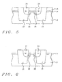
- a conductive material 22 is then formed over the structure.
- the conductive material 22 is preferably doped and can be doped polysilicon, epitarial silicon, or polysilicon. This doped conductive material 22, is usually deposited doped polysilicon, and is about 500 to 1500 and preferably 1000 Angstroms thick from the top of the structure, see 23 of Fig. 4.
- the doped conductive material 22 is then chemically mechanically polished to form a doped conductive mass 24 (e.g., Source and Drain regions) .
- a doped conductive mass 24 e.g., Source and Drain regions
- Fig 6 shows the removal of the etch block 16, preferably by a selective hot phosphoric acid strip etch.
- polysilicon oxidation is preformed usually in an oxidation furnace to create a polyoxidation 26.
- the polyoxidation is between 180 and 220 Angstroms thick.
- Spacers 28 are then formed and are about 900 to 1100 angstroms thick. These spacers are usually made of an oxide or a nitride, and preferably a nitride.
- the spacers are formed by a conventional blanket deposition and an isotropic etch back.
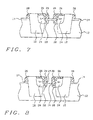
- FIG 9 illustrates a gate dielectric (e.g., oxide) layer 30 is then formed preferably by deposition.
- This gate dielectric layer 30 is preferably a high K oxide material such as silicon nitride, silicon oxide, tantolum oxide, zirconium oxide, or hafnium oxide.
- Fig. 10 illustrates a gate electrode material 32 is then formed usually by deposition, and then chemically mechanically polished down.
- the gate electrode material 32 is can be metal, metal silicide, or polysilicon, and is preferably Polysilicon.
- the doped conductive material 22, can alternatively be just conductive material when applied to the structure and then doped after the structure looks like Fig. 10. This doping of conductive material 22, can be done using a masked implant step.
Landscapes
- Insulated Gate Type Field-Effect Transistor (AREA)
- Electrodes Of Semiconductors (AREA)
- Element Separation (AREA)
Applications Claiming Priority (2)
| Application Number | Priority Date | Filing Date | Title |
|---|---|---|---|
| US764241 | 2001-01-19 | ||
| US09/764,241 US6380088B1 (en) | 2001-01-19 | 2001-01-19 | Method to form a recessed source drain on a trench side wall with a replacement gate technique |
Publications (2)
| Publication Number | Publication Date |
|---|---|
| EP1225623A2 true EP1225623A2 (de) | 2002-07-24 |
| EP1225623A3 EP1225623A3 (de) | 2006-06-07 |
Family
ID=25070108
Family Applications (1)
| Application Number | Title | Priority Date | Filing Date |
|---|---|---|---|
| EP02368006A Withdrawn EP1225623A3 (de) | 2001-01-19 | 2002-01-18 | Ein Verfahren zur Herstellung von auf einem Grabenwand begrabene Source und Drain mittels einen Austauschgatter-Technik |
Country Status (5)
| Country | Link |
|---|---|
| US (1) | US6380088B1 (de) |
| EP (1) | EP1225623A3 (de) |
| JP (1) | JP4070469B2 (de) |
| SG (1) | SG98042A1 (de) |
| TW (1) | TW523819B (de) |
Cited By (1)
| Publication number | Priority date | Publication date | Assignee | Title |
|---|---|---|---|---|
| CN102891170A (zh) * | 2011-07-19 | 2013-01-23 | 中芯国际集成电路制造(上海)有限公司 | Ldmos晶体管结构及其制造方法 |
Families Citing this family (9)
| Publication number | Priority date | Publication date | Assignee | Title |
|---|---|---|---|---|
| US6621131B2 (en) | 2001-11-01 | 2003-09-16 | Intel Corporation | Semiconductor transistor having a stressed channel |
| US6924517B2 (en) * | 2003-08-26 | 2005-08-02 | International Business Machines Corporation | Thin channel FET with recessed source/drains and extensions |
| US7208803B2 (en) * | 2004-05-05 | 2007-04-24 | Taiwan Semiconductor Manufacturing Company, Ltd. | Method of forming a raised source/drain and a semiconductor device employing the same |
| US7037795B1 (en) * | 2004-10-15 | 2006-05-02 | Freescale Semiconductor, Inc. | Low RC product transistors in SOI semiconductor process |
| US7202535B2 (en) * | 2005-07-14 | 2007-04-10 | Infineon Technologies Ag | Manufacturing method for an integrated semiconductor structure and corresponding integrated semiconductor structure |
| KR100762231B1 (ko) | 2005-09-15 | 2007-10-01 | 주식회사 하이닉스반도체 | 리세스채널을 갖는 반도체소자의 제조방법 |
| RU2360265C1 (ru) * | 2008-05-20 | 2009-06-27 | Государственное образовательное учреждение высшего профессионального образования "Пензенский государственный университет" (ПГУ) | Способ радиолокационного обнаружения подвижных целей с фазовой селекцией по дальности и устройство для его реализации |
| US8476131B2 (en) | 2011-08-24 | 2013-07-02 | Globalfoundries Inc. | Methods of forming a semiconductor device with recessed source/design regions, and a semiconductor device comprising same |
| US8383473B1 (en) | 2012-04-12 | 2013-02-26 | Globalfoundries Inc. | Methods of forming replacement gate structures for semiconductor devices |
Family Cites Families (11)
| Publication number | Priority date | Publication date | Assignee | Title |
|---|---|---|---|---|
| US5455189A (en) * | 1994-02-28 | 1995-10-03 | National Semiconductor Corporation | Method of forming BICMOS structures |
| US5380671A (en) | 1994-06-13 | 1995-01-10 | United Microelectronics Corporation | Method of making non-trenched buried contact for VLSI devices |
| US5643822A (en) | 1995-01-10 | 1997-07-01 | International Business Machines Corporation | Method for forming trench-isolated FET devices |
| KR0151051B1 (ko) | 1995-05-30 | 1998-12-01 | 김광호 | 반도체장치의 절연막 형성방법 |
| US5834360A (en) * | 1996-07-31 | 1998-11-10 | Stmicroelectronics, Inc. | Method of forming an improved planar isolation structure in an integrated circuit |
| US5710076A (en) * | 1996-09-03 | 1998-01-20 | Industrial Technology Research Institute | Method for fabricating a sub-half micron MOSFET device with global planarization of insulator filled shallow trenches, via the use of a bottom anti-reflective coating |
| US5879998A (en) | 1997-07-09 | 1999-03-09 | Advanced Micro Devices, Inc. | Adaptively controlled, self-aligned, short channel device and method for manufacturing same |
| US5920095A (en) * | 1997-07-30 | 1999-07-06 | Motorola, Inc. | Short channel field effect semiconductor device and method of making |
| US6225659B1 (en) * | 1998-03-30 | 2001-05-01 | Advanced Micro Devices, Inc. | Trenched gate semiconductor device and method for low power applications |
| US6071783A (en) * | 1998-08-13 | 2000-06-06 | Taiwan Semiconductor Manufacturing Company | Pseudo silicon on insulator MOSFET device |
| US6214670B1 (en) * | 1999-07-22 | 2001-04-10 | Taiwan Semiconductor Manufacturing Company | Method for manufacturing short-channel, metal-gate CMOS devices with superior hot carrier performance |
-
2001
- 2001-01-19 US US09/764,241 patent/US6380088B1/en not_active Expired - Lifetime
- 2001-11-26 SG SG200107305A patent/SG98042A1/en unknown
-
2002
- 2002-01-04 TW TW091100049A patent/TW523819B/zh not_active IP Right Cessation
- 2002-01-18 EP EP02368006A patent/EP1225623A3/de not_active Withdrawn
- 2002-01-21 JP JP2002011494A patent/JP4070469B2/ja not_active Expired - Fee Related
Cited By (2)
| Publication number | Priority date | Publication date | Assignee | Title |
|---|---|---|---|---|
| CN102891170A (zh) * | 2011-07-19 | 2013-01-23 | 中芯国际集成电路制造(上海)有限公司 | Ldmos晶体管结构及其制造方法 |
| CN102891170B (zh) * | 2011-07-19 | 2015-04-01 | 中芯国际集成电路制造(上海)有限公司 | Ldmos晶体管结构及其制造方法 |
Also Published As
| Publication number | Publication date |
|---|---|
| SG98042A1 (en) | 2003-08-20 |
| JP4070469B2 (ja) | 2008-04-02 |
| EP1225623A3 (de) | 2006-06-07 |
| TW523819B (en) | 2003-03-11 |
| JP2002314075A (ja) | 2002-10-25 |
| US6380088B1 (en) | 2002-04-30 |
Similar Documents
| Publication | Publication Date | Title |
|---|---|---|
| US6476444B1 (en) | Semiconductor device and method for fabricating the same | |
| KR100822079B1 (ko) | 단일 면 매립 스트랩 | |
| EP1069613B1 (de) | Auf geringe Leckage ausgerichtete Architektur für sub 0,18 Mikrometer salizidiertes CMOS Bauelement | |
| US6340614B1 (en) | Method of forming a DRAM cell | |
| KR100507856B1 (ko) | Mos트랜지스터 제조방법 | |
| US6235593B1 (en) | Self aligned contact using spacers on the ILD layer sidewalls | |
| US6380088B1 (en) | Method to form a recessed source drain on a trench side wall with a replacement gate technique | |
| US6534370B2 (en) | Method for fabricating a semiconductor device having an elevated source/drain scheme | |
| JPH07106560A (ja) | 溝型半導体装置とその製造方法 | |
| JPH0621210A (ja) | 半導体装置の製造方法 | |
| KR20040069515A (ko) | 리세스 채널 mosfet 및 그 제조방법 | |
| US6232160B1 (en) | Method of delta-channel in deep sub-micron process | |
| JP2003060069A (ja) | 二重ゲート酸化膜を有する半導体素子の製造方法 | |
| KR100845103B1 (ko) | 반도체소자의 제조방법 | |
| US6077761A (en) | Method for fabricating a transistor gate with a T-like structure | |
| US7179713B2 (en) | Method of fabricating a fin transistor | |
| US6642592B2 (en) | Semiconductor device and method for fabricating same | |
| KR20020055147A (ko) | 반도체 소자의 제조방법 | |
| JPH1197529A (ja) | 半導体装置の製造方法 | |
| JPH0729971A (ja) | 半導体装置の製造方法 | |
| KR100344837B1 (ko) | 반도체 소자 및 그의 제조방법 | |
| KR100271661B1 (ko) | 반도체 소자 제조방법 | |
| KR100317311B1 (ko) | 반도체소자 및 그의 제조방법 | |
| JPH06244415A (ja) | 半導体装置およびその製造方法 | |
| KR100323725B1 (ko) | 반도체소자 및 그의 제조방법 |
Legal Events
| Date | Code | Title | Description |
|---|---|---|---|
| PUAI | Public reference made under article 153(3) epc to a published international application that has entered the european phase |
Free format text: ORIGINAL CODE: 0009012 |
|
| AK | Designated contracting states |
Kind code of ref document: A2 Designated state(s): AT BE CH CY DE DK ES FI FR GB GR IE IT LI LU MC NL PT SE TR |
|
| AX | Request for extension of the european patent |
Free format text: AL;LT;LV;MK;RO;SI |
|
| RAP1 | Party data changed (applicant data changed or rights of an application transferred) |
Owner name: CHARTERED SEMICONDUCTOR MANUFACTURING LTD. |
|
| PUAL | Search report despatched |
Free format text: ORIGINAL CODE: 0009013 |
|
| AK | Designated contracting states |
Kind code of ref document: A3 Designated state(s): AT BE CH CY DE DK ES FI FR GB GR IE IT LI LU MC NL PT SE TR |
|
| AX | Request for extension of the european patent |
Extension state: AL LT LV MK RO SI |
|
| AKX | Designation fees paid | ||
| REG | Reference to a national code |
Ref country code: DE Ref legal event code: 8566 |
|
| STAA | Information on the status of an ep patent application or granted ep patent |
Free format text: STATUS: THE APPLICATION IS DEEMED TO BE WITHDRAWN |
|
| 18D | Application deemed to be withdrawn |
Effective date: 20061208 |