EP1229365A2 - Connection par alignement passif pour fibres optiques - Google Patents
Connection par alignement passif pour fibres optiques Download PDFInfo
- Publication number
- EP1229365A2 EP1229365A2 EP02000953A EP02000953A EP1229365A2 EP 1229365 A2 EP1229365 A2 EP 1229365A2 EP 02000953 A EP02000953 A EP 02000953A EP 02000953 A EP02000953 A EP 02000953A EP 1229365 A2 EP1229365 A2 EP 1229365A2
- Authority
- EP
- European Patent Office
- Prior art keywords
- fiber optic
- waveguides
- accordance
- substrate
- fibers
- Prior art date
- Legal status (The legal status is an assumption and is not a legal conclusion. Google has not performed a legal analysis and makes no representation as to the accuracy of the status listed.)
- Withdrawn
Links
Images


Classifications
-
- G—PHYSICS
- G02—OPTICS
- G02B—OPTICAL ELEMENTS, SYSTEMS OR APPARATUS
- G02B6/00—Light guides; Structural details of arrangements comprising light guides and other optical elements, e.g. couplings
-
- G—PHYSICS
- G02—OPTICS
- G02B—OPTICAL ELEMENTS, SYSTEMS OR APPARATUS
- G02B6/00—Light guides; Structural details of arrangements comprising light guides and other optical elements, e.g. couplings
- G02B6/24—Coupling light guides
- G02B6/26—Optical coupling means
- G02B6/30—Optical coupling means for use between fibre and thin-film device
-
- G—PHYSICS
- G02—OPTICS
- G02B—OPTICAL ELEMENTS, SYSTEMS OR APPARATUS
- G02B6/00—Light guides; Structural details of arrangements comprising light guides and other optical elements, e.g. couplings
- G02B6/24—Coupling light guides
- G02B6/36—Mechanical coupling means
- G02B6/38—Mechanical coupling means having fibre to fibre mating means
- G02B6/3807—Dismountable connectors, i.e. comprising plugs
- G02B6/3873—Connectors using guide surfaces for aligning ferrule ends, e.g. tubes, sleeves, V-grooves, rods, pins, balls
- G02B6/3882—Connectors using guide surfaces for aligning ferrule ends, e.g. tubes, sleeves, V-grooves, rods, pins, balls using rods, pins or balls to align a pair of ferrule ends
-
- G—PHYSICS
- G02—OPTICS
- G02B—OPTICAL ELEMENTS, SYSTEMS OR APPARATUS
- G02B6/00—Light guides; Structural details of arrangements comprising light guides and other optical elements, e.g. couplings
- G02B6/10—Light guides; Structural details of arrangements comprising light guides and other optical elements, e.g. couplings of the optical waveguide type
- G02B6/12—Light guides; Structural details of arrangements comprising light guides and other optical elements, e.g. couplings of the optical waveguide type of the integrated circuit kind
- G02B6/12007—Light guides; Structural details of arrangements comprising light guides and other optical elements, e.g. couplings of the optical waveguide type of the integrated circuit kind forming wavelength selective elements, e.g. multiplexer, demultiplexer
- G02B6/12009—Light guides; Structural details of arrangements comprising light guides and other optical elements, e.g. couplings of the optical waveguide type of the integrated circuit kind forming wavelength selective elements, e.g. multiplexer, demultiplexer comprising arrayed waveguide grating [AWG] devices, i.e. with a phased array of waveguides
- G02B6/12019—Light guides; Structural details of arrangements comprising light guides and other optical elements, e.g. couplings of the optical waveguide type of the integrated circuit kind forming wavelength selective elements, e.g. multiplexer, demultiplexer comprising arrayed waveguide grating [AWG] devices, i.e. with a phased array of waveguides characterised by the optical interconnection to or from the AWG devices, e.g. integration or coupling with lasers or photodiodes
-
- G—PHYSICS
- G02—OPTICS
- G02B—OPTICAL ELEMENTS, SYSTEMS OR APPARATUS
- G02B6/00—Light guides; Structural details of arrangements comprising light guides and other optical elements, e.g. couplings
- G02B6/24—Coupling light guides
- G02B6/36—Mechanical coupling means
- G02B6/38—Mechanical coupling means having fibre to fibre mating means
- G02B6/3807—Dismountable connectors, i.e. comprising plugs
- G02B6/3873—Connectors using guide surfaces for aligning ferrule ends, e.g. tubes, sleeves, V-grooves, rods, pins, balls
- G02B6/3885—Multicore or multichannel optical connectors, i.e. one single ferrule containing more than one fibre, e.g. ribbon type
Definitions
- This invention generally relates to fiber optic systems, especially connection techniques and devices. More particularly, the invention relates to technology which is suitable for use in optical multiplexing and demultiplexing. Included are so-called dense wavelength division multiplexing (DWDM) products.
- DWDM dense wavelength division multiplexing
- optical frequency waves generated by sources such as light emitting diode (LED) units, lasers, and the like.
- Optical fibers typically are fabricated of glass materials and, as optical fiber circuitry has developed, it has become necessary to provide connecting devices which can couple one optical fiber to another. It is important that the connection be in an end-to-end aligned relationship.
- a traditional procedure for making a connection between ends of optical fibers is to initially remove a protective jacket from a given length of fiber at the end of the fiber to be joined. After the jacket is removed, a 250 micron (outside diameter) buffer is exposed which then can be stripped to expose a 125 micron (outer diameter) fiber.
- the fiber body then is threaded through a passage in a ferrule where it is affixed in place by adhesive and/or crimping. The fiber is inserted so as to extend well beyond a front surface of the ferrule. The exposed fiber material then is cleaved and polished. Any remaining adhesive is removed.
- the ferrules then are assembled into a connector assembly which is intended to position the optical fibers with their optical axes in alignment for connection to the fibers of a mating connector or other appropriate connecting device.
- Fiber optic ribbon cable has become increasingly popular to provide multiple channels in a single cable structure.
- An optical ribbon cable is similar to any other well-known ribbon electrical cable to the extent that a plurality of optical fibers or channels are disposed in a line or a generally coplanar relationship.
- prior art practice for terminating the optical fibers of a fiber optic ribbon cable is generally similar to the procedure summarized above.
- the unitary protective jacket surrounding the line of fibers is removed so that the buffered fibers are exposed which then are stripped such that the unprotected fibers project from the flat cable in a line.
- these individual fibers must be inserted into respective individual holes or passages in a prefabricated connector ferrule. The passages align the fibers at a predetermined spacing for coupling to the ends of the fibers in a complementary connector ferrule or other connecting device.
- connector ferrules In the prior art, placing individual fibers of a multi-fiber cable into individual holes or passages in a connector ferrule results in a high percentage of rejects.
- the ferrules must be inspected hole by hole. In addition to fibers being broken, the holes themselves may be too large or too small, or not circular, or have some other defect.
- Connector ferrules comprise bodies which are crystalline in nature, typically of ceramic material. Instead, they can be molded of a plastic or polymeric material.
- the fiber-receiving holes or passages must be formed precisely to maintain a proper form or alignment and spacing between the fibers in order to prevent tolerance problems causing transmission losses during mating.
- Alignment problems and tolerance problems such as those noted above are further complicated in connector assemblies wherein a pair of mating connector ferrules themselves are placed into mating condition by two alignment pins. These alignment pins typically have one end of each pin extending into a passage of the connector ferrule, and the opposite end of the pin is inserted into a passage in the mating connector ferrule, with a chamfered lead-in on the pin for alignment.
- the problems of maintaining precise tolerances with the alignment pins and their passages must be added to the tolerance problems in maintaining precise spacing and alignment of the individual holes for the optical fibers of the fiber optic cable. It can be understood why there are such a high number of rejects during the application of prior art connector units.
- multiplexing can be used to combine channels of different wavelengths, whereas at the receiving end demultiplexing separates the channels from one another with a minimum inter-channel cross talk.
- the separation between adjacent devices is designed to be fairly narrow in order to increase device capacity.
- a typical separation is 200 GHz to 50 GHz, corresponding to 1.6 nm and 0.4 nm in wavelength, respectively.
- Currently available DWDM products are of the arrayed waveguide (AWG) type, such as of the 1 x 8 (1 input, 8 outputs) 1 x 16, 1 x 32 and 1 x 64 configurations. It will be appreciated that a small difference among the lengths of the output waveguides is responsible for separating the stream of wavelengths from one another.
- a fiber optic connector ferrule is useful in precisely aligning a line of fibers for alignment with a complementary ferrule.
- An example of such an approach and of a type of fixture for assembling same is shown in Bunin et al. U. S. Patent No. 5,907,657, incorporated hereinto by reference. While ferrules of this type are an important advance in the art, further improvements are realized according to the present invention which achieves an advantageously passive alignment requiring no light up or monitoring of light in the fibers.
- the passive alignment process of the invention is fast, reproducible, easy and cost effective. So advanced is this approach that accurate alignment according to the invention is achievable in the field by straightforward component removal and replacement. This is a marked improvement over prior art approaches which require alignment in a laboratory environment, typically requiring very expensive alignment equipment.
- passive alignment fiber optic connection is accomplished using a modular approach.
- a fiber optic connection system which combines a connector receptacle such as a ferrule together with a receptor substrate which has a plurality of waveguides. The respective ends of these waveguides are positioned such that they are in precise alignment with spacing and positioning of respective ends of the connector receptacle fibers.
- the substrate can be a chip such as an AWG type of DWDM. It is important to note that the invention avoids the traditional approach of laying fiber optic fibers onto the substrate chip or within grooves of the substrate chip or other component.
- projecting pins and complementary pin passages orient proper alignment and help to secure that alignment.
- the invention provides center-to-center alignment between respective ends of fiber optic fibers in one component and respective ends of waveguides of another component when these components are connected to each other.
- Another object of this invention is to provide an approved fiber optic connection component which is readily installed in the field and does not require laboratory conditions or expensive equipment.
- Another object of the present invention is to provide an improved system and method which permits replacement of only damaged or faulty components, or those suspected of being faulty, rather than requiring replacement of an entire assembly.
- Another object of this invention is an improved system and method which provide a modular approach to fiber optic connection.
- Another object of the present invention is to provide an improved chip substrate structure that is a waveguide substrate which neither utilizes fiber optic fibers at points of connection nor receives fiber optic fibers from other components.
- a connector receptacle or connector ferrule 21 is in general position for aligning assembly with one attachment location of a substrate 22, shown in exploited form in this view.
- Another connector receptacle 23 likewise is shown in a general mating alignment with a different attachment location of the substrate 22.
- Each attachment location provides a connection location at which passive alignment takes place, as explained more fully elsewhere herein.
- substrate 22 has an input end 24 and an output end 25.
- the illustrated input end is arranged for accommodating a relatively low number of optical channels 26, while the illustrated output end accommodates a greater number of optical channels 27.
- connector receptacle 23 has a fiber optic cable 28 having a relatively low number of optical fibers, while the fiber optic cable 29 has a higher number of optical fibers.
- the number of fibers in each fiber optic cable can vary as required for communication with the particular substrate or chip.
- both fiber optic cables 28 and 29 can contain the same number of optical fibers.
- a typical fiber optic ribbon can have 12 fibers, for example.
- the substrate 22 of Fig. 1 can be seen as an illustration of a 1 x 12 AWG type DWDM product.
- other combinations of input channels and output channels are contemplated.
- the illustrated connector ferrule 21 is shown in more detail in Fig. 2. Fibers 31 of the fiber optic cable 29 are shown. Ends 32 of these fibers are illustrated at the mating face 33. A ferrule body 34 also is shown. Attachment pins in the connector component or in the substrate component are provided to mate with pin passageways in the other component. In the illustrated embodiment, the pins are on the connector component, and the pin passageways or receptors are in the substrate component. As shown, two attachment pins 35 project from the face 33. In a typical assembly each pin 35 is secured within a pin passage 36.
- pins 35 preferably are precision cylindrical pins having a round cross-section, a typical standard pin in this regard having a diameter of 700 microns, plus or minus 1 micron.
- a suitable connector receptacle can be made in accordance with Bunin et al. U. S. Patent No. 5,907,651, incorporated by reference hereinto.
- Fig. 2 shows a typical suitable example of an empty connector and of its component parts.
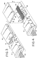
- Fig. 3, Fig. 4 and Fig. 5 show a portion of the assembly or system of Fig. 1. Only one connector is shown, and the substrate is shown in simplified form in order to illustrated important aspects of the invention. For purposes of illustration, these views show what can be considered to be a portion of the substrate 22 of Fig. 1. For purposes of illustration, this will be identified as a substrate output portion 37.
- This substrate 37 is composed of two principal structural components, namely an upper wafer 38 and a lower wafer 39, as viewed in the drawings.
- waveguide locations 42 can be formed into the wafer assembly (as shown), or they can be locations which are present between wafers without requiring any channels, grooves or the like formed into a wafer. It is important to note that these waveguide locations are present or are formed without requiring the laying of any optical fibers thereat.
- each waveguide location 42 includes a waveguide channel 43 containing a waveguide 44.
- each waveguide channel 43 is triangular in cross-section and is formed into the upper wafer, as viewed in the drawings.
- each waveguide 44 is positioned on the lower wafer, as viewed in the drawings. As is typical of waveguides, those illustrated are of a square cross section.
- Each of the upper wafer 38 and the lower wafer 39 are made of suitable available materials, and their respective features can be made or located by incorporating generally known techniques and materials. After fabrication, these wafers are secured to each other to form the waveguide substrate 37.
- channels 43 When channels 43 are formed in the upper wafer 38 for example, they typically are formed by means of an etching procedure, such as one incorporating the use of potassium hydroxide. Precise positing of the channels 43 and of upper portions 45 of the pin passageways can be accomplished by using photoresist and masking techniques and known photolithographic types of procedures. This type of approach accomplishes the predetermined alignment pattern discussed herein with respect to the channels and passageways of the upper wafer 38.
- the location of the waveguides 44 and of lower portions 46 of the pin passageways 41 in the lower wafer 39 can be formed by known techniques in order to provide the predetermined alignment pattern characteristic of the waveguide substrate 37. Examples of specific processing steps which can be incorporated in forming the features of the waveguide substrate can be found in Yamane et al. U. S. Patent No. 5,557,695, which is incorporated hereinto by reference. As needed, multiple layers having different refraction indices, typically formed by suitable deposition techniques, can be incorporated. Usually the substrate body is a silicon substrate. Mask patterns having the precise predetermined alignment pattern and spacing typically will be deposited by vapor deposition, sputtering, or some other suitable approach. Typically, these are used in association with an etching procedure. Appropriate energy sources are used, and several steps may be incorporated, in order to complete formation of the predetermined alignment pattern of the waveguide substrate.
- the waveguides typically are formed of sol-gel materials, silicon dioxide materials, or other suitable material.
- the predetermined alignment pattern which is characteristic of the waveguide substrate module 37 is duplicated by an alignment pattern of the fiber ends 32 and the attachment pins 35 of each connector module 21. This is illustrated more particularly by reference to Fig. 6, to Fig. 7 and to Fig. 8.
- Fig. 6 illustrates a typical predetermined alignment pattern of the waveguide substrate 37.
- Ends of the waveguides 44 are precisely spaced and aligned with respect to each other and with respect to pin passageways 41, more particularly the respective centers thereof.
- these ends of the waveguides also are in alignment with respect to mating face 47 of the waveguide substrate. There is no need for the waveguides to project beyond this mating face 47. In an important embodiment, these waveguide ends are flush with this mating face.
- This alignment pattern of the waveguide ends and pin passageways 41 of the waveguide substrate 37 is duplicated in the connector 21. More specifically, fiber ends 32, more particularly the respective centers thereof, follow the identical predetermined alignment pattern of the ends of the waveguides 44. Preferably, these ends 32 of the optical fibers also are in alignment with respect to mating face 33 of the connector module. There is no need for the fibers to project beyond this mating face 33. In an important embodiment, these fiber ends are flush with this mating face.
- the precise predetermined alignment pattern which is characteristic of the pin passageways 41 of the waveguide substrate module is precisely repeated for the attachment pins 35 of the connector module, more particularly the respective centers of the passageways 41 and pins 35.
- pins 35 are inserted into pin passageways 41, there is passively achieved precise center-to-center alignment of each optical waveguide end with each respective optical fiber end.
- Whole registry of these respective ends is facilitated by center-to-center alignment of the respective attachment pins 35 and pin passageways 41, in conjunction with a precise sizing of pins 35 and pin passageways 41 which allows for sliding insertion while avoiding play or movement of the pins within the pin passageways.
- Fig. 7 shows waveguide channels 43 accommodating waveguides 44.
- a suitable filler 48 such as a set epoxy, other adhesive, or other suitable filler material, can be included as shown.
- Ends of the optic fibers 31 are shown in broken lines in Fig. 7 in order to illustrate the passive center-to-center alignment which is achieved according to the invention.
- Each end includes a fiber core 51, which is surrounded by body 52 of the fiber itself. This same relationship is shown from an opposite point of view in Fig. 8. It will be appreciated that the relative sizing between the fibers and the waveguide is not to scale in Fig. 7 and Fig. 8.
- each waveguide has a side width of about 7 microns, while each fiber core 51 has a diameter of about 9 microns.
- a typical fiber body 52 has an outer diameter of about 125 microns.
- a typical cladding which has been removed therefrom at this location of the connector 21 has an outer diameter of about 250 microns.
- the ends 32 of the fibers, and thus the fiber cores 51 and fiber bodies 52, do not project beyond the mating face 33 of each connector 21. This helps to protect the fibers and to assure that they remain in the predetermined alignment pattern because they are fully supported by the mating face 33. Typically, ends 32 are flush with the mating face 33, with the fibers being embedded within the connector 21.
- an epoxy or other suitable filler which sets is used.
- An assembly procedure such as this is instrumental in maintaining the needed alignment.
- an assembly approach such as this includes polishing the ends and at least a portion of the mating face, which helps to insure a smooth, planer surface for alignment mating with face 47 which opposes face 33 after assembly of a connector with the waveguide substrate.
- any optical fiber there is no requirement for any optical fiber to enter into a receptor of any kind such as a channel associated with the waveguide substrate.
- a receptor of any kind such as a channel associated with the waveguide substrate.
- any optical waveguide to enter into the connector.
- the passively aligned connection which is characteristic of the invention can be rendered more stable and secure by attaching together the mating faces 33 and 47.
- Any suitable attachment means is possible, including a setting adhesive or other glue-type component, specifically including an epoxy adhesive system.
- Such attachment preferably is at or near the periphery of the engaging faces, so as to not interfere with the optical communication between the fiber ends and the waveguide ends.
- the present invention avoids the labor intensive, tedious and potentially imprecise laying down of optical fibers in order to make an optical fiber connection, which typically is accomplished successfully only in a laboratory environment. Instead, with the present invention, a component such as a connector module or a chip module which is damaged or suspected as being defective is removed, such as by pulling the components apart while sliding the attachment pins 35 out of the pin passageways 41, followed by reinsertion after appropriate replacement. This can be accomplished in the field, rather than requiring return to a manufacturing facility or laboratory environment in order to achieve the needed connection when replacements or repairs are needed. Moreover, this field work can be in the nature of "trouble shooting" work during which modules can be exchanged until the defective component is identified and replaced.
Landscapes
- Physics & Mathematics (AREA)
- General Physics & Mathematics (AREA)
- Optics & Photonics (AREA)
- Optical Couplings Of Light Guides (AREA)
- Mechanical Coupling Of Light Guides (AREA)
Applications Claiming Priority (2)
| Application Number | Priority Date | Filing Date | Title |
|---|---|---|---|
| US09/760,682 US6986608B2 (en) | 2001-01-16 | 2001-01-16 | Passive alignment connection for fiber optics |
| US760682 | 2001-01-16 |
Publications (2)
| Publication Number | Publication Date |
|---|---|
| EP1229365A2 true EP1229365A2 (fr) | 2002-08-07 |
| EP1229365A3 EP1229365A3 (fr) | 2005-01-19 |
Family
ID=25059852
Family Applications (1)
| Application Number | Title | Priority Date | Filing Date |
|---|---|---|---|
| EP02000953A Withdrawn EP1229365A3 (fr) | 2001-01-16 | 2002-01-16 | Connection par alignement passif pour fibres optiques |
Country Status (5)
| Country | Link |
|---|---|
| US (1) | US6986608B2 (fr) |
| EP (1) | EP1229365A3 (fr) |
| JP (1) | JP3738441B2 (fr) |
| KR (1) | KR100418842B1 (fr) |
| CN (1) | CN100367059C (fr) |
Cited By (4)
| Publication number | Priority date | Publication date | Assignee | Title |
|---|---|---|---|---|
| EP1548472A1 (fr) * | 2003-12-22 | 2005-06-29 | Rohm and Haas Electronic Materials, L.L.C. | Procédé et dispositif de couplage de fibres optiques et de guides d'onde integrés dans une carte imprimée |
| WO2014095391A1 (fr) * | 2012-12-19 | 2014-06-26 | Reichle & De-Massari Ag | Plaque à circuit imprimé optique |
| EP2955556A1 (fr) * | 2014-06-09 | 2015-12-16 | Corning Optical Communications LLC | Coupleur à facette latérale ayant une surface de montage externe moulée pour faciliter l'alignement de connexions optiques |
| WO2018165002A1 (fr) * | 2017-03-07 | 2018-09-13 | Corning Optical Communications LLC | Corps de connecteurs femelles destinés à des puces optiques et connexions optiques incorporant lesdits corps |
Families Citing this family (32)
| Publication number | Priority date | Publication date | Assignee | Title |
|---|---|---|---|---|
| KR100526505B1 (ko) * | 2003-06-24 | 2005-11-08 | 삼성전자주식회사 | 광도파로와 광학소자의 결합 구조 및 이를 이용한 광학정렬 방법 |
| US7427166B2 (en) * | 2004-09-27 | 2008-09-23 | Adamant Kogyo Co., Ltd. | Neutral gender MT-type ferrule, adapter, and polishing method |
| CN100449343C (zh) * | 2006-04-03 | 2009-01-07 | 浙江博创科技有限公司 | 一种新颖高精度光纤阵列的制造方法 |
| CN100520462C (zh) * | 2006-06-16 | 2009-07-29 | 亿光电子工业股份有限公司 | 光耦合器的制造方法 |
| US20080298748A1 (en) * | 2007-05-31 | 2008-12-04 | Terry Dean Cox | Direct-connect optical splitter module |
| US20080298743A1 (en) * | 2007-05-31 | 2008-12-04 | Konstantinos Saravanos | Microsplitter module for optical connectivity |
| US8798427B2 (en) | 2007-09-05 | 2014-08-05 | Corning Cable Systems Llc | Fiber optic terminal assembly |
| US20090110345A1 (en) * | 2007-10-26 | 2009-04-30 | International Business Machines Corporation | Methods for passive micrometer-range alignment of components using removable reference structures |
| US7382954B1 (en) | 2007-10-26 | 2008-06-03 | International Business Machines Corporation | Methods for passive micrometer-range alignment of components using removable reference structures |
| EP2344915A4 (fr) | 2008-10-09 | 2015-01-21 | Corning Cable Sys Llc | Terminal à fibre optique ayant un panneau adaptateur portant à la fois les fibres d'entrée et de sortie provenant d'un diviseur optique |
| US8879882B2 (en) | 2008-10-27 | 2014-11-04 | Corning Cable Systems Llc | Variably configurable and modular local convergence point |
| WO2010082967A1 (fr) * | 2009-01-14 | 2010-07-22 | Molex Incorporated | Connecteur résistant aux intempéries, modules électriques et leurs ensembles résistant aux intempéries |
| EP2237091A1 (fr) | 2009-03-31 | 2010-10-06 | Corning Cable Systems LLC | Terminal à fibres optiques pouvant être assemblé de manière amovible |
| US8467651B2 (en) * | 2009-09-30 | 2013-06-18 | Ccs Technology Inc. | Fiber optic terminals configured to dispose a fiber optic connection panel(s) within an optical fiber perimeter and related methods |
| US9547144B2 (en) | 2010-03-16 | 2017-01-17 | Corning Optical Communications LLC | Fiber optic distribution network for multiple dwelling units |
| US8792767B2 (en) | 2010-04-16 | 2014-07-29 | Ccs Technology, Inc. | Distribution device |
| US9547145B2 (en) | 2010-10-19 | 2017-01-17 | Corning Optical Communications LLC | Local convergence point for multiple dwelling unit fiber optic distribution network |
| US9219546B2 (en) | 2011-12-12 | 2015-12-22 | Corning Optical Communications LLC | Extremely high frequency (EHF) distributed antenna systems, and related components and methods |
| US8724937B2 (en) * | 2011-12-20 | 2014-05-13 | International Business Machines Corporation | Fiber to wafer interface |
| US10110307B2 (en) | 2012-03-02 | 2018-10-23 | Corning Optical Communications LLC | Optical network units (ONUs) for high bandwidth connectivity, and related components and methods |
| US9004778B2 (en) | 2012-06-29 | 2015-04-14 | Corning Cable Systems Llc | Indexable optical fiber connectors and optical fiber connector arrays |
| US9049500B2 (en) | 2012-08-31 | 2015-06-02 | Corning Cable Systems Llc | Fiber optic terminals, systems, and methods for network service management |
| US8909019B2 (en) | 2012-10-11 | 2014-12-09 | Ccs Technology, Inc. | System comprising a plurality of distribution devices and distribution device |
| US9243784B2 (en) | 2012-12-20 | 2016-01-26 | International Business Machines Corporation | Semiconductor photonic package |
| US9400356B2 (en) | 2013-03-14 | 2016-07-26 | International Business Machines Corporation | Fiber pigtail with integrated lid |
| US8923665B2 (en) | 2013-03-15 | 2014-12-30 | International Business Machines Corporation | Material structures for front-end of the line integration of optical polarization splitters and rotators |
| US10042125B2 (en) * | 2015-07-06 | 2018-08-07 | Xyratex Technology Limited | Optical connectors |
| CN105278056B (zh) * | 2015-11-06 | 2017-05-03 | 武汉电信器件有限公司 | 一种波分复用/解复用光组件 |
| US10151888B2 (en) * | 2017-03-29 | 2018-12-11 | Mellanox Technologies, Ltd. | Optical waveguide structure |
| JP2019215405A (ja) * | 2018-06-11 | 2019-12-19 | 日本電信電話株式会社 | 光ファイバ接続部品および光デバイスの作製方法 |
| US20210271037A1 (en) * | 2020-02-28 | 2021-09-02 | Corning Research & Development Corporation | Optical-electrical substrate providing interconnects for photonic integrated circuit and associated methods |
| WO2021247994A1 (fr) * | 2020-06-05 | 2021-12-09 | Siphox, Inc. | Systèmes et procédés pour couplage de puce photonique |
Family Cites Families (16)
| Publication number | Priority date | Publication date | Assignee | Title |
|---|---|---|---|---|
| JP3133474B2 (ja) * | 1992-03-18 | 2001-02-05 | 古河電気工業株式会社 | ガイド溝付き光導波路の製作方法 |
| JPH0618744A (ja) | 1992-04-27 | 1994-01-28 | Nippon Telegr & Teleph Corp <Ntt> | 光分岐ユニット及びこのユニットに用いる導波路型光カプラモジュール |
| JPH05333231A (ja) | 1992-05-29 | 1993-12-17 | Furukawa Electric Co Ltd:The | 光導波路と光ファイバの接続方法 |
| JPH0772347A (ja) * | 1993-06-17 | 1995-03-17 | Furukawa Electric Co Ltd:The | ガイド溝付き光導波路の製作方法 |
| US5400423A (en) * | 1993-09-07 | 1995-03-21 | Motorola | Molded star coupler and method of making same |
| SE503905C2 (sv) | 1994-03-16 | 1996-09-30 | Ericsson Telefon Ab L M | Förfarande för framställning av en optokomponent samt optokomponent |
| SE513183C2 (sv) | 1994-03-18 | 2000-07-24 | Ericsson Telefon Ab L M | Förfarande för framställning av en optokomponent samt kapslad optokomponent |
| US5602951A (en) | 1994-04-14 | 1997-02-11 | Sumitomo Electric Industries, Ltd. | Ferrule for optical connector and process for making same |
| JPH0829638A (ja) | 1994-05-12 | 1996-02-02 | Fujitsu Ltd | 光導波路・光ファイバ接続構造及び光導波路・光ファイバ接続方法並びに光導波路・光ファイバ接続に使用される光導波路基板及び同基板の製造方法並びに光導波路・光ファイバ接続に使用されるファイバ基板付き光ファイバ |
| JP2851796B2 (ja) | 1994-07-28 | 1999-01-27 | 日本碍子株式会社 | 光ファイバアレイの基板への固定方法 |
| JPH08278425A (ja) | 1995-04-07 | 1996-10-22 | Furukawa Electric Co Ltd:The | 光導波路モジュールの製造方法 |
| JPH0990158A (ja) * | 1995-09-28 | 1997-04-04 | Furukawa Electric Co Ltd:The | 光モジュール及びその組立方法 |
| US5613024A (en) * | 1995-12-21 | 1997-03-18 | Lucent Technologies Inc. | Alignment of optical fiber arrays to optical integrated circuits |
| US5907651A (en) | 1997-07-28 | 1999-05-25 | Molex Incorporated | Fiber optic connector ferrule |
| JP3850569B2 (ja) * | 1998-12-09 | 2006-11-29 | 富士通株式会社 | フェルールアセンブリ及び光モジュール |
| CA2258398A1 (fr) * | 1999-01-07 | 2000-07-07 | Victor Benham | Systeme d'assemblage sans adhesif de fibres optiques a lentille integree sur guide d'ondes optique |
-
2001
- 2001-01-16 US US09/760,682 patent/US6986608B2/en not_active Expired - Fee Related
-
2002
- 2002-01-15 CN CNB021077134A patent/CN100367059C/zh not_active Expired - Fee Related
- 2002-01-16 JP JP2002044019A patent/JP3738441B2/ja not_active Expired - Fee Related
- 2002-01-16 KR KR10-2002-0002463A patent/KR100418842B1/ko not_active Expired - Fee Related
- 2002-01-16 EP EP02000953A patent/EP1229365A3/fr not_active Withdrawn
Cited By (7)
| Publication number | Priority date | Publication date | Assignee | Title |
|---|---|---|---|---|
| EP1548472A1 (fr) * | 2003-12-22 | 2005-06-29 | Rohm and Haas Electronic Materials, L.L.C. | Procédé et dispositif de couplage de fibres optiques et de guides d'onde integrés dans une carte imprimée |
| US7292756B2 (en) | 2003-12-22 | 2007-11-06 | Rohm And Haas Electronics Materials Llc | Optical interface assembly and method of formation |
| WO2014095391A1 (fr) * | 2012-12-19 | 2014-06-26 | Reichle & De-Massari Ag | Plaque à circuit imprimé optique |
| EP2955556A1 (fr) * | 2014-06-09 | 2015-12-16 | Corning Optical Communications LLC | Coupleur à facette latérale ayant une surface de montage externe moulée pour faciliter l'alignement de connexions optiques |
| US9645327B2 (en) | 2014-06-09 | 2017-05-09 | Corning Optical Communications LLC | Side-facet coupler having external mounting surface molded to facilitate alignment of optical connections |
| WO2018165002A1 (fr) * | 2017-03-07 | 2018-09-13 | Corning Optical Communications LLC | Corps de connecteurs femelles destinés à des puces optiques et connexions optiques incorporant lesdits corps |
| US20190384019A1 (en) * | 2017-03-07 | 2019-12-19 | Corning Optical Communications LLC | Receptacle bodies for optical chips and optical connections incorporating the same |
Also Published As
| Publication number | Publication date |
|---|---|
| CN1369723A (zh) | 2002-09-18 |
| JP2002311286A (ja) | 2002-10-23 |
| CN100367059C (zh) | 2008-02-06 |
| US20050238290A1 (en) | 2005-10-27 |
| EP1229365A3 (fr) | 2005-01-19 |
| JP3738441B2 (ja) | 2006-01-25 |
| US6986608B2 (en) | 2006-01-17 |
| KR20020061539A (ko) | 2002-07-24 |
| KR100418842B1 (ko) | 2004-02-14 |
Similar Documents
| Publication | Publication Date | Title |
|---|---|---|
| US6986608B2 (en) | Passive alignment connection for fiber optics | |
| US20250093608A1 (en) | Flexible optical circuit, cassettes, and methods | |
| US10365439B2 (en) | Optical interconnect | |
| EP3807686B1 (fr) | Connecteurs optiques et ensembles connecteurs optiques détachables destinés à des puces optiques | |
| US5790733A (en) | Optoelectronic device receptacle and method of making same | |
| US5519799A (en) | Optical fiber array structure | |
| US6241399B1 (en) | Ferrule assembly and optical module | |
| EP3816689B1 (fr) | Connecteurs d'unité de réseau de fibres utilisant un alignement broche à broche | |
| US5970192A (en) | Method of aligning optical waveguide device | |
| US6210047B1 (en) | Method of fabricating a fiber optic connector ferrule | |
| US6767136B1 (en) | Device having multiple optical fibers | |
| US20240329320A1 (en) | Dense photonic integrated circuit optical edge coupling | |
| JP2004078028A (ja) | 光ファイバガイド部品およびその作製方法 | |
| WO2003005085A1 (fr) | Integration d'un coupleur collimate par verre fondu dans des modules optoelectroniques | |
| US20230176286A1 (en) | Optical components and optical connectors having a splice-on connection and method of fabricating the same | |
| JP2001264577A (ja) | 光部品及びその製造方法並びに光部品用ウエハ及びその製造方法 |
Legal Events
| Date | Code | Title | Description |
|---|---|---|---|
| PUAI | Public reference made under article 153(3) epc to a published international application that has entered the european phase |
Free format text: ORIGINAL CODE: 0009012 |
|
| AK | Designated contracting states |
Kind code of ref document: A2 Designated state(s): AT BE CH CY DE DK ES FI FR GB GR IE IT LI LU MC NL PT SE TR |
|
| AX | Request for extension of the european patent |
Free format text: AL;LT;LV;MK;RO;SI |
|
| PUAL | Search report despatched |
Free format text: ORIGINAL CODE: 0009013 |
|
| AK | Designated contracting states |
Kind code of ref document: A3 Designated state(s): AT BE CH CY DE DK ES FI FR GB GR IE IT LI LU MC NL PT SE TR |
|
| AX | Request for extension of the european patent |
Extension state: AL LT LV MK RO SI |
|
| RIC1 | Information provided on ipc code assigned before grant |
Ipc: 7G 02B 6/30 A |
|
| 17P | Request for examination filed |
Effective date: 20050624 |
|
| AKX | Designation fees paid |
Designated state(s): DE FR GB IT |
|
| STAA | Information on the status of an ep patent application or granted ep patent |
Free format text: STATUS: THE APPLICATION IS DEEMED TO BE WITHDRAWN |
|
| 18D | Application deemed to be withdrawn |
Effective date: 20100803 |