EP1235103B1 - Methode zur Naheffekt-Korrektur mit teilweise strahlungsdurchlässigen, nicht aufgelösten Hilfsstrukturen - Google Patents
Methode zur Naheffekt-Korrektur mit teilweise strahlungsdurchlässigen, nicht aufgelösten Hilfsstrukturen Download PDFInfo
- Publication number
- EP1235103B1 EP1235103B1 EP02251316A EP02251316A EP1235103B1 EP 1235103 B1 EP1235103 B1 EP 1235103B1 EP 02251316 A EP02251316 A EP 02251316A EP 02251316 A EP02251316 A EP 02251316A EP 1235103 B1 EP1235103 B1 EP 1235103B1
- Authority
- EP
- European Patent Office
- Prior art keywords
- features
- resolvable
- mask
- optical proximity
- proximity correction
- Prior art date
- Legal status (The legal status is an assumption and is not a legal conclusion. Google has not performed a legal analysis and makes no representation as to the accuracy of the status listed.)
- Expired - Lifetime
Links
Images






Classifications
-
- G—PHYSICS
- G03—PHOTOGRAPHY; CINEMATOGRAPHY; ANALOGOUS TECHNIQUES USING WAVES OTHER THAN OPTICAL WAVES; ELECTROGRAPHY; HOLOGRAPHY
- G03F—PHOTOMECHANICAL PRODUCTION OF TEXTURED OR PATTERNED SURFACES, e.g. FOR PRINTING, FOR PROCESSING OF SEMICONDUCTOR DEVICES; MATERIALS THEREFOR; ORIGINALS THEREFOR; APPARATUS SPECIALLY ADAPTED THEREFOR
- G03F1/00—Originals for photomechanical production of textured or patterned surfaces, e.g., masks, photo-masks, reticles; Mask blanks or pellicles therefor; Containers specially adapted therefor; Preparation thereof
- G03F1/36—Masks having proximity correction features; Preparation thereof, e.g. optical proximity correction [OPC] design processes
-
- H—ELECTRICITY
- H10—SEMICONDUCTOR DEVICES; ELECTRIC SOLID-STATE DEVICES NOT OTHERWISE PROVIDED FOR
- H10P—GENERIC PROCESSES OR APPARATUS FOR THE MANUFACTURE OR TREATMENT OF DEVICES COVERED BY CLASS H10
- H10P76/00—Manufacture or treatment of masks on semiconductor bodies, e.g. by lithography or photolithography
-
- G—PHYSICS
- G03—PHOTOGRAPHY; CINEMATOGRAPHY; ANALOGOUS TECHNIQUES USING WAVES OTHER THAN OPTICAL WAVES; ELECTROGRAPHY; HOLOGRAPHY
- G03F—PHOTOMECHANICAL PRODUCTION OF TEXTURED OR PATTERNED SURFACES, e.g. FOR PRINTING, FOR PROCESSING OF SEMICONDUCTOR DEVICES; MATERIALS THEREFOR; ORIGINALS THEREFOR; APPARATUS SPECIALLY ADAPTED THEREFOR
- G03F1/00—Originals for photomechanical production of textured or patterned surfaces, e.g., masks, photo-masks, reticles; Mask blanks or pellicles therefor; Containers specially adapted therefor; Preparation thereof
- G03F1/50—Mask blanks not covered by G03F1/20 - G03F1/34; Preparation thereof
-
- G—PHYSICS
- G03—PHOTOGRAPHY; CINEMATOGRAPHY; ANALOGOUS TECHNIQUES USING WAVES OTHER THAN OPTICAL WAVES; ELECTROGRAPHY; HOLOGRAPHY
- G03F—PHOTOMECHANICAL PRODUCTION OF TEXTURED OR PATTERNED SURFACES, e.g. FOR PRINTING, FOR PROCESSING OF SEMICONDUCTOR DEVICES; MATERIALS THEREFOR; ORIGINALS THEREFOR; APPARATUS SPECIALLY ADAPTED THEREFOR
- G03F7/00—Photomechanical, e.g. photolithographic, production of textured or patterned surfaces, e.g. printing surfaces; Materials therefor, e.g. comprising photoresists; Apparatus specially adapted therefor
- G03F7/70—Microphotolithographic exposure; Apparatus therefor
- G03F7/70425—Imaging strategies, e.g. for increasing throughput or resolution, printing product fields larger than the image field or compensating lithography- or non-lithography errors, e.g. proximity correction, mix-and-match, stitching or double patterning
- G03F7/70433—Layout for increasing efficiency or for compensating imaging errors, e.g. layout of exposure fields for reducing focus errors; Use of mask features for increasing efficiency or for compensating imaging errors
- G03F7/70441—Optical proximity correction [OPC]
Definitions
- the present invention relates to photolithography, and in particular to the design and generation of a photomask ("mask”) having sub-resolution optical proximity correction (“OPC”) features, which function to correct for optical proximity effects and increase the overall processing performance.
- the present invention also relates to the use of such a mask in a lithographic projection apparatus, which generally comprises:
- Lithographic apparatus can be used, for example, in the manufacture of integrated circuits (ICs).
- the mask may contain a circuit pattern corresponding to an individual layer of the IC, and this pattern can be imaged onto a target portion (e.g. comprising one or more dies) on a substrate (silicon wafer) that has been coated with a layer of radiation-sensitive material (resist).
- a target portion e.g. comprising one or more dies
- a substrate silicon wafer
- a layer of radiation-sensitive material resist
- a single wafer will contain a whole network of adjacent target portions that are successively irradiated via the projection system, one at a time.
- each target portion is irradiated by exposing the entire mask pattern onto the target portion in one go; such an apparatus is commonly referred to as a wafer stepper.
- each target portion is irradiated by progressively scanning the mask pattern under the projection beam in a given reference direction (the "scanning" direction) while synchronously scanning the substrate table parallel or anti-parallel to this direction; since, in general, the projection system will have a magnification factor M (generally ⁇ 1), the speed V at which the substrate table is scanned will be a factor M times that at which the mask table is scanned.
- M magnification factor
- a mask pattern is imaged onto a substrate that is at least partially covered by a layer of radiation-sensitive material (resist).
- the substrate Prior to this imaging step, the substrate may undergo various procedures, such as priming, resist coating and a soft bake. After exposure, the substrate may be subjected to other procedures, such as a post-exposure bake (PEB), development, a hard bake and measurement/inspection of the imaged features.
- PEB post-exposure bake
- This array of procedures is used as a basis to pattern an individual layer of a device, e.g. an IC.
- the projection system may hereinafter be referred to as the "lens"; however, this term should be broadly interpreted as encompassing various types of projection systems, including refractive optics, reflective optics, and catadioptric systems, for example.
- the radiation system may also include components operating according to any of these design types for directing, shaping or controlling the projection beam of radiation, and such components may also be referred to below, collectively or singularly, as a "lens".
- the lithographic apparatus may be of a type having two or more substrate tables (and/or two or more mask tables). In such "multiple stage" devices the additional tables may be used in parallel, or preparatory steps may be carried out on one or more tables while one or more other tables are being used for exposures.
- the photolithographic masks referred to above comprise geometric patterns corresponding to the circuit components to be integrated onto a silicon wafer.
- the patterns used to create such masks are generated utilizing CAD (computer-aided design) programs, this process often being referred to as EDA (electronic design automation).
- EDA electronic design automation
- Most CAD programs follow a set of predetermined design rules in order to create functional masks. These rules are set by processing and design limitations.
- design rules define the space tolerance between circuit devices (such as gates, capacitors, etc.) or interconnect lines, so as to ensure that the circuit devices or lines do not interact with one another in an undesirable way.
- the design rule limitations are typically referred to as "critical dimensions" (CD).
- a critical dimension of a circuit can be defined as the smallest width of a line or the smallest space between two lines. Thus, the CD determines the overall size and density of the designed circuit.
- the CD of its corresponding mask pattern approaches the resolution limit of the optical exposure tool.
- the resolution for an exposure tool is defined as the minimum feature that the exposure tool can repeatedly expose on the wafer.
- the resolution value of present exposure equipment often constrains the CD for many advanced IC circuit designs.
- Sub-lithographic features have dimensions less than the resolution of the exposure tool, and therefore do not transfer to the photoresist layer. Instead, sub-lithographic features interact with the original mask pattern and compensate for proximity effects, thereby improving the final transferred circuit pattern.
- sub-lithographic features examples include scattering bars and anti-scattering bars which are added to mask patterns to reduce differences between features within a mask pattern caused by proximity effects.
- sub-resolution assist features, or scattering bars have been used as a means to correct for optical proximity effects and have been shown to be effective for increasing the overall process window (i.e., the ability to consistently print features having a specified CD regardless of whether or not the features are isolated or densely packed relative to adjacent features).
- the optical proximity correction occurs by improving the depth of focus for the less dense to isolated features by placing scattering bars near these features.
- the scattering bars function to change the effective pattern density (of the isolated or less dense features) to be more dense, thereby negating the undesirable proximity effects associated with printing of isolated or less dense features. It is important, however, that the scattering bars themselves do not print on the wafer. Thus, this requires that the size of the scattering bars must be maintained below the resolution capability of the imaging system.
- US 6,048,647 discloses a photolithography mask having a plurality of resolvable features and a non-resolvable feature disposed between two of the resolvable features, the non-resolvable feature having a transmission coefficient of between 0% and 100%.
- the present invention provides a method of designing a photolithography mask for optically transferring a pattern formed in said mask onto a substrate, said method comprising:
- the gray bars which have a transmission value variable between 0-100%, are positioned between the features on the mask so as to control the magnitude of diffraction orders received by a collection lens, specifically to minimise the second order diffraction component of the grey bars, thereby allowing for the control of imaging characteristics of individual features on the mark. Further, by controlling the width, placement and transmission values of the grey bar assist features the present invention allows for features having various line:space duty ratios to be printed utilizing the same process window.
- the present invention provides significant improvements and advantages over prior art OPC techniques. For example, by utilizing gray bar assist features having a width smaller than the width of the space between the features, and by controlling the size, transmission, location and spatial frequency of the gray bar assist features, the diffraction energy in the collection lens can be modified to allow for image enhancement which improves upon the image enhancement obtainable utilizing prior art OPC techniques. More specifically, by manipulating the dimensions and transmission coefficient of the gray bar assist features, the present invention allows for features having various line:space duty ratios to be printed utilizing the same process window, while simultaneously minimizing the likelihood that the assist feature will print.
- the plurality of resolvable features may include densely spaced features and non-densely spaced features, the non-resolvable optical proximity correction features being disposed between the non-densely spaced features.
- the transmission coefficient of the non-resolvable optical proximity correction features is then adjusted such that the difference between an isofocal inflection point associated with the non-densely spaced resolvable features and an isofocal inflection point associated with the densely spaced resolvable features is minimised.
- the terms "radiation” and “beam” are used to encompass all types of electromagnetic radiation, including ultraviolet radiation (e.g. with a wavelength of 365, 248, 193, 157 or 126 nm) and EUV (extreme ultra-violet radiation, e.g. having a wavelength in the range 5-20 nm).
- mask as employed in this text may be broadly interpreted as referring to generic patterning means that can be used to endow an incoming radiation beam with a patterned cross-section, corresponding to a pattern that is to be created in a target portion of the substrate; the term "light valve" can also be used in this context.
- classic mask transmissive or reflective; binary, phase-shifting, hybrid, etc.
- examples of other such patterning means include:
- non-resolvable gray bar assist features having a transmission which can vary from 0-100% are utilized as sub-resolution assist features.
- the use of the gray bar assist features designed by the present invention allows for an improvement in the process overlap (i.e., the ability to print dense and semi-isolated features utilizing the same process).
- Fig. 1 is helpful in understanding one of the problems solved by the present invention, which relates to imaging small features across a range of line:space duty ratios.
- the figure illustrates simulated aerial images for two imaging scenarios.
- 150nm lines having a 1:1 line:space duty ratio i.e., dense features
- the line:space duty ratio is changed to 1:3.5 (i.e., semi-isolated images).
- Both the 1:1 dense features and the 1:3.5 semi-isolated features are shown at best focus and with 300nm of defocus.
- the simulated aerial images of Fig. 1 illustrate problems associated with imaging geometries of varying line:space duty ratio.
- the dense features generally suffer from poor contrast, and yet are less affected by variations in defocus because of the location of the image's isofocal inflection point.
- the isofocal inflection point corresponds to the location at which the image prints with minimal losses regardless of whether the image is printed with substantially no defocus (i.e., best focus) or with 300nm of defocus.
- the isofocal inflection point 12 falls dimensionally close to the position of the mask edge.
- the 1:3.5 semi-isolated features exhibit higher contrast, but suffer from defocus and aberration effects.
- the present invention provides a method for achieving the foregoing objective so as to allow dense and non-dense features to be printed utilizing the same process window, while simultaneously minimizing the likelihood that the assist features will print.
- the present invention utilizes the gray bar assist features to modify/manipulate the values of these diffraction orders so as to drive the isofocal inflection point and the image intensity of the less dense features toward that of the dense features, thereby providing for an improvement in the process overlap.
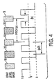
- Fig. 4 illustrates one example of how the gray bar assist features can be utilized to vary the isofocal inflection point and the image intensity of the less dense features toward that of the dense features.
- a gray bar assist feature 18 is positioned between each feature 20 to be printed.
- the gray bar assist features 18 need not be placed between every feature contained on a given mask, but only those for which it is desirable to provide OPC (e.g., the non-dense features).
- the effect that the gray bar assist features 18 have on the magnitude of the zero, first and second diffraction orders can be calculated for the mask such as that shown in Fig. 4. More specifically, for opaque main features 20 and non-attenuating clear openings, the magnitude of the orders become: Mag .
- zero order [ 1 - ( b / s ) 1 - ⁇ I b ] s / p Mag .
- first order ( s / p ) sinc ( s / p ) - 1 - ⁇ I b ⁇ b / p ⁇ sinc b / p Mag .
- the zero, first and second diffraction orders can be manipulated/adjusted by controlling the width and/or the intensity of the gray bar assist feature 18. As mentioned above and explained in more detail below, the manipulation of these diffraction orders allows the isofocal inflection point and the image intensity of the less dense features to be driven toward that of the dense features.
- Figs. 5(b)-5(e) illustrate resulting diffraction patterns for gray bar assist features 18 utilized in the mask illustrated in Fig. 5(a), which contains 150nm features having a space of 375nm between features 20.
- the gray bar assist features 18 have a width 1/3 of the space dimension.
- Four variations of the gray bar assist features 18 are illustrated in Figs. 5(b)-5(e), 100% transmission (Fig. 5(b)), 50% transmission (Fig. 5(c)), 25% transmission (Fig. 5(d)) and 0% transmission (Fig. 5(e)).
- the 0% transmission case corresponds to the scatter bar assist feature, as disclosed in USP No. 5,821,014, when the scatter bar dimension is small enough such that it does not print.
- the maximum width of scatter bars is approximately 1/3 the value of the exposure wavelength. Accordingly, as the wavelength of the exposing source continues to decrease, it becomes exceedingly difficult to fabricate scatter bar assist features that remain sub-resolution.
- the width of the gray bar assist feature is not limited to such a sub-resolution width.
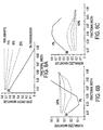
- Figs. 6(a)-6(c) illustrate how the primary diffraction orders (i.e., 0, 1st and 2nd) are influenced by the gray bar assist features of the present invention.
- the zero order magnitude values (Fig. 6(a)) are plotted along with the first order magnitude (Fig. 6(b)) and the second order magnitude (Fig. 6(c)) values normalized to the resulting value of the zero order.
- the plots correspond to features having a 1:2.5 line:space duty ratio with gray bar assist features ranging from zero width to a width equal to the entire space opening in the mask.
- a fractional bar width of zero implies no bar, and a fractional width of 1.00 implies a full space width bar.
- the transmission of the gray bars is variable from 0% (binary) to 100% (no bar).
- the gray bar assist features by utilizing the gray bar assist features it is possible to control the magnitude of the second diffraction order so as to prevent the printing of the assist features which would otherwise occur.
- the second diffraction order corresponding to the scatter bar (0% transmission) exhibits a large increase relative to the gray bar assist features, which indicates that the scatter bar is more likely to print than the gray bar.
- the gray bar assist features also provide for a decrease in the zero diffraction order and a decrease in the first diffraction order, which advantageously functions to drive the isofocal inflection point and the image intensity of the 1:2.5 duty ratio features to that of the more dense features.
- Figs. 7(a)-7(c) illustrate "equivalent solutions" for known scatter bars and gray bar assist features of the present invention.
- the feature width and spacing and the imaging conditions utilized in conjunction with the images of Figs. 7(a)-7(c) are the same as those described above in conjunction with the images of Figs. 6(a)-6(c).
- the zero order magnitude values (Fig. 7(a)) are plotted along with the first order magnitude (Fig. 7(b)) and the second order magnitude (Fig. 7(c)) values normalized to the resulting value of the zero order.
- the zero order magnitude of a scatter bar having a fractional width of 0.17 is substantially equivalent to a gray bar having a fractional width of 0.33 and 25% transmission, and is also substantially equivalent to a gray bar having a fractional width of 0.50 and 50% transmission.
- Fig. 7(c) it is shown that the magnitude of the second diffraction order for the scatter bar increases significantly relative to the second diffraction order of the gray bar assist features, which significantly increases the likelihood of the printing of the scatter bar.
- the gray bar assist features of the present invention eliminate this problem by allowing for widths significantly larger than that of the corresponding equivalent scatter bar.
- Figs. 8(a)-8(d) illustrate simulated aerial images for a 150nm wide feature having a line:space duty ratio of 1:2.5, which are imaged with a 248nm wavelength, a 0.70 lens pupil NA, and a partial coherence value (sigma) of 0.85. Each image is plotted for 0 defocus to 300nm of defocus.
- Fig. 8(a) illustrates the results without utilizing any gray bar assist features. As shown, the resulting image isofocal inflection value of the resulting image is 0.71.
- Figs. 8(b)-8(d) illustrate three gray bar solutions for the 1:2.5 duty ratio features of Fig. 8(a) that result in equivalent zero order reduction. Specifically, Fig.
- Fig. 8(b) corresponds to a 0% transmission gray bar (i.e., a scatter bar) with a 0.17 fractional width
- Fig. 8(c) corresponds to a 25% transmission gray bar with a 33% fractional width
- Fig. 8(d) corresponds to a 44% transmission gray bar with a 50% fractional width.
- the isofocal inflection point for each solution is 0.45, which represents a reduction in the isofocal inflection point relative to the non-corrected feature shown in Fig. 8(a).
- the intensity of the bar region (I BAR ) for the 44% transmitting 0.5 width bar is 16% larger than that for the 0.17 fractional width bar.
- the I BAR for the 25% transmission gray bar with a 33% fractional width is also greater than that for the 0.17 fractional width bar.
- the likelihood that the gray bar assist features of Fig. 8(c) or Fig. 8(d) will print is significantly reduced in comparison to that of the equivalent scatter bar version of Fig. 8(b).
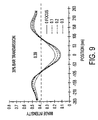
- Fig. 9 illustrates how the gray bar assist features can be tuned to further decrease the isofocal inflection point in comparison to the reduction illustrated in Fig. 8(d).
- the gray bar assist feature utilized to generate the aerial image was a 30% transmission gray bar with a fractional width of 50%. All other imaging conditions, feature width and feature line:space ratio are the same as utilized in Fig. 8(d). As shown, the isofocal inflection point is reduced an additional 13% to a value of 0.39 and the printability of the bar remains low due to the dampened second diffraction order.
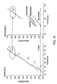
- Fig. 10 illustrates the effect of various gray bar assist features on a 150nm feature having a line:space duty ratio of 1:2.5.
- the use of the gray bar assist feature provides an improvement by reducing the isofocal inflection point and the resulting CD of the 1:2.5 feature to closer to that of the 1:1 feature.
- this reduction in the isofocal inflection point and the resulting CD allows for an increase in across pitch process overlap.
- the gray bars designed by the method of the present invention allow for the matching of printing performance of more isolated features to that of more dense features, while simultaneously minimizing the chance that the assist feature will print.
- the gray bars accomplish this by allowing for some transmission within the assist bars and by preserving spatial frequency by using a single bar between features, thereby providing for more adjustment of the isofocal inflection points.
- gray bar assist features there are numerous possible methods for fabricating the gray bar assist features.
- one solution is the use of half-tone features as small sub-resolution masking elements placed relative to one another such that first diffraction orders of the elements are not collected with the imaging tool.
- the size of the sub-resolution elements are small enough so that only the DC component of the diffraction pattern contributes to image formation.
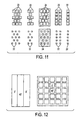
- These sub-resolution elements can consist of small islands 22 or holes 24, such as those shown in Fig. 11. The sizing and pitch of these features are adjusted to achieve the desired transmission values within the gray bar.
- a half-tone gray bar can be fabricated using sub- ⁇ or super- ⁇ phase-shifted elements on a sub-resolution grid as illustrated in Fig. 12. Phase islands of 40, 60, 80 and 100 degrees result in transmission values of 12%, 25%, 42% and 60%, respectively.
- a multilayer mask structure can also be utilized to form the gray bar assist features.
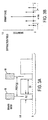
- an amorphous Si or a Si-rich silicon layer 32 is formed on a quartz substrate 30, and a conventional anti-reflective (AR) chrome masking layer 34 is formed on the amorphous silicon (Si) layer so as to allow for dual tone masking.
- the amorphous Si layer is patterned as the gray bar masking level and the AR chrome layer is patterned as the main feature level.
- the thickness of the amorphous Si layer is adjusted so that transmission falls within the desired gray bar range, which, for example, corresponds to a thickness between 30 angstroms and 300 angstroms.
- the mask can be fabricated, for example, using conventional multiple-level electron beam and patterning processes.
- a mask substrate is pre-deposited with the amorphous Si and AR chrome layers.
- a positive acting electron-sensitive polymer is coated over the deposited substrate.
- An electron beam is used to expose areas where neither the main features or the gray bar features will exist.
- the polymer is removed in the exposed regions and the AR chrome and the amorphous Si are removed from the openings.
- a second patterning step is carried out which involves a second coating of electron sensitive polymer; electron beam exposure of gray bar regions only; and etching of the AR chrome from the amorphous Si gray bars.
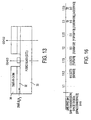
- gray bar assist features designed by the method of the present invention in combination with an attenuated phase-shift mask (APSM).
- APSM phase-shift mask
- first order [ 1 + ⁇ T ]
- second order [ 1 + ⁇ T ]
- Figs. 14(a)-(c) are plots of the primary diffraction orders resulting from the combination of an opaque assist bar (scatter bar) with APSM for features having a 1:2.5 line:space duty ratio.
- APSM values are varied from 0% (binary) to 20%.
- the scatter bar widths are varied from zero to the full space width. As set forth above, a practical limit of a single scatter bar may be 0.15 to 0.20 of the space width opening. The results indicate that by combining opaque assist bars with APSM, increased APSM transmission can be utilized. For example, a 10% APSM using a 0.17 width SB results in side lobes equivalent to those for a 6% APSM without assist bars.
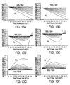
- Figs. 15(a)-(f) illustrate two APSM examples combined with gray bar assist features designed by the method of the present invention.
- Figs. 15(a)-(c) are of the zero, normalized first and normalized second diffraction order values, respectively, for a feature having a 1:2.5 line:space duty ratio and 6% APSM with various gray bar widths and gray bar transmissions.
- Figs. 15(d)-(f) illustrate the same, with the exception being the use of 18% APSM.
- the results set forth in Figs. 15(a)-(f) illustrate how APSM reduces the value of the zero order while increasing the value of the first order and impacting the value of the second order to a lesser degree.
- gray bar assist features reduces the zero order as well as the first order, thereby decreasing the likelihood of such side-lobe effects.
- the gray bar assist features designed by the method of the present invention allow for an increase in process overlap by reducing the isofocal inflection point and resulting CD of non-dense features closer to that of dense features.
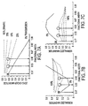
- gray bar solutions were present for features having line:space duty ratio values between 1:1.2 and 1:3.5 using the primary diffraction order evaluation equations. This approach allows for these solutions to be generated prior to any lithographic simulation or imaging.
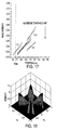
- Fig. 16 summarizes the results including the line bias required for each feature and the gray bar dimension for a 50% transmission value. It is noted that preferably, the bar width is always centered within the space opening and the widths vary from 50nm for the 1:1.2 features up to 220nm for the 1:3.5 features.
- FIG. 17 illustrates the improved imaging results obtained utilizing these gray bar solutions. It is noted that the results set forth in Fig. 17 also utilized a custom illumination as illustrated in Fig. 18. As shown, the isofocal slices for all line:space duty ratios were brought close to that for the 1:1 features, with respect to both intensity and position.
- the 1:2 duty ratio case was a problem pitch as a result of the pitch of the features being a multiple of 1.5X of the 1:1 features optimized with the foregoing illumination condition.
- the illumination condition places the first diffraction order of the 1:2 duty ratio features in the center of the objective lens pupil, resulting in a maximum defocus aberration effect when combined with its corresponding zero order.
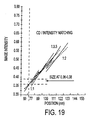
- a second gray bar solution was performed to compensate for this problematic pitch effect and resulting image is shown in Fig. 19.
- the present invention provides significant advantages over known OPC assist features. Most importantly, by manipulating the dimensions and transmission coefficient of the gray bar assist features, the present invention allows for features having various line:space duty ratios to be printed utilizing the same process window, while simultaneously minimizing the likelihood that the assist feature will print.
- the gray bar assist features can be utilized with off-axis illumination techniques, such as quadrapole illumination.
- an analytical model for determining the optimum combination or optical-image enhancement is an analytical method of utilizing the mask electric field character and the resulting diffraction energy distribution produced from imaging situations using one or more optical-image enhancement (OE) techniques.
- OE optical-image enhancement
- Mask modifications can be related to their impact on these fundamental orders.
- Illumination can be related to the distribution and specific collection of these orders.
- Aberration effects (including defocus) can be combined to account for phase variations of the diffraction orders. By analyzing these effects in the frequency domain of the lens, design and optimization is possible. This design and optimization method can be incorporated into a computer program.
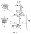
- Fig. 20 schematically depicts a lithographic projection apparatus suitable for use with a mask designed with the aid of the current invention.
- the apparatus comprises:
- the apparatus is of a transmissive type (i.e. has a transmissive mask). However, in general, it may also be of a reflective type, for example (with a reflective mask). Alternatively, the apparatus may employ another kind of patterning means as an alternative to the use of a mask; examples include a programmable mirror array or LCD matrix.
- the source LA e.g. a mercury lamp or excimer laser
- This beam is fed into an illumination system (illuminator) IL, either directly or after having traversed conditioning means, such as a beam expander Ex, for example.
- the illuminator IL may comprise adjusting means AM for setting the outer and/or inner radial extent (commonly referred to as ⁇ -outer and ⁇ -inner, respectively) of the intensity distribution in the beam.
- ⁇ -outer and ⁇ -inner commonly referred to as ⁇ -outer and ⁇ -inner, respectively
- it will generally comprise various other components, such as an integrator IN and a condenser CO.
- the beam PB impinging on the mask MA has a desired uniformity and intensity distribution in its cross-section.
- the source LA may be within the housing of the lithographic projection apparatus (as is often the case when the source LA is a mercury lamp, for example), but that it may also be remote from the lithographic projection apparatus, the radiation beam that it produces being led into the apparatus (e.g. with the aid of suitable directing mirrors); this latter scenario is often the case when the source LA is an excimer laser (e.g. based on KrF, ArF or F 2 lasing).
- the current invention encompasses both of these scenarios.
- the depicted tool can be used in two different modes:
Landscapes
- Physics & Mathematics (AREA)
- General Physics & Mathematics (AREA)
- Exposure And Positioning Against Photoresist Photosensitive Materials (AREA)
- Preparing Plates And Mask In Photomechanical Process (AREA)
Claims (8)
- Verfahren zur Erzeugung einer Photolithographie-Maske (MA) zur optischen Übertragung eines Musters, das in der Maske (MA) gebildet wird, auf ein Substrat (W), wobei das Verfahren folgendes umfasst :- Anordnung einer Vielzahl auflösbarer Strukturen (20), die auf das Substrat gedruckt werden sollen ; und- Anordnung einer Vielzahl nicht auflösbarer Strukturen der Naheffekt-Korrektur (18), die jeweils zwischen einem Paar der Vielzahl auflösbarer Strukturen (20) angeordnet sind, wobei die nicht auflösbare Struktur der Naheffekt-Korrektur (18) einen Übertragungskoeffizienten von größer 0 % und kleiner als 100 % besitzt ;gekennzeichnet durch Auswahl des Übertragungskoeffizienten der nicht auflösbaren Struktur der Naheffekt-Korrektur (18), um eine Beugungskomponente der zweiten Ordnung, die der nicht auflösbaren Struktur der Naheffekt-Korrektur (18) entspricht, zu minimieren.
- Verfahren nach Anspruch 1, wobei die nicht auflösbare Struktur der Naheffekt-Korrektur eine Breitenabmessung besitzt, die geringer ist als die Breite eines Abstandes, der zwei der Vielzahl von auflösbaren Strukturen (20) voneinander trennt.
- Verfahren nach einem der vorhergehenden Ansprüche, wobei die nicht auflösbare Struktur der Naheffekt-Korrektur (18) in der Mitte des Abstandes angeordnet ist, der zwei der Vielzahl von auflösbaren Strukturen (20) voneinander trennt.
- Verfahren zur Herstellung einer Photolithographie-Maske (MA), das die Verfahrensschritte der Entwicklung der Photolithographie-Maske durch ein Verfahren gemäß einem der Ansprüche 1 bis 3 umfasst.
- Computerprogramm mit Programm-Code-Elementen, um einen Computer anzuweisen, mindestens eine Datei zu erzeugen, die einer Photolithographie-Maske (MA) entspricht, um ein Muster mit einer Vielzahl auflösbarer Strukturen (20), die auf das Substrat gedruckt werden sollen, das in der Maske auf dem Substrat gebildet wird, optisch zu übertragen, wobei das Programm folgendes umfasst :- Code-Elemente zur Definition einer Vielzahl nicht auflösbarer Strukturen der Naheffekt-Korrektur (18), die zwischen Paaren der Vielzahl auflösbarer Strukturen angeordnet sind ; und- Code-Elemente zur Auswahl des Übertragungskoeffizienten der nicht auflösbaren Struktur der Naheffekt-Korrektur (18) innerhalb des Bereichs von größer 0 % und kleiner als 100 %, um eine Beugungskomponente der zweiten Ordnung, die der nicht auflösbaren Struktur der Naheffekt-Korrektur (18) entspricht, zu minimieren.
- Computerprogramm nach Anspruch 5 mit Code-Elementen zur Definition der nicht auflösbaren Strukturen der Naheffekt-Korrektur mit einer Breitenabmessung von weniger als der Breite eines Abstandes, der die beiden auflösbaren Strukturen der Vielzahl der auflösbaren Strukturen (20) voneinander trennt.
- Computerprogramm nach Anspruch 5 oder 6 mit Code-Elementen zur Anordnung der nicht auflösbaren Strukturen der Naheffekt-Korrektur (18) in der Mitte des Abstandes, der das Paar der Vielzahl auflösbarer Strukturen (20) voneinander trennt.
- Verfahren zur Herstellung eines Bausteins, das die nachfolgenden Schritte umfasst :(a) Bereitstellen eines Substrates (W), das zumindest teilweise von einer Schicht aus strahlungsempfindlichem Material bedeckt ist ;(b) Bereitstellen eines Projektionsstrahls (PB) der Strahlung unter Verwendung eines Bestrahlungssystems ;(c) Verwenden eines Musters auf einer Maske (MA), um den Projektionsstrahl (PB) in seinem Querschnitt mit einem Muster zu versehen;(d) Projizieren des bemusterten Strahls der Strahlung auf einen Zielabschnitt der Schicht aus strahlungsempfindlichem Material ;
wobei das Verfahren weiterhin die folgenden Schritte umfasst :(e) Herstellen einer Photolithographie-Maske nach dem Verfahren von Anspruch 4.
Applications Claiming Priority (2)
| Application Number | Priority Date | Filing Date | Title |
|---|---|---|---|
| US27188001P | 2001-02-27 | 2001-02-27 | |
| US271880P | 2001-02-27 |
Publications (3)
| Publication Number | Publication Date |
|---|---|
| EP1235103A2 EP1235103A2 (de) | 2002-08-28 |
| EP1235103A3 EP1235103A3 (de) | 2003-08-06 |
| EP1235103B1 true EP1235103B1 (de) | 2007-04-18 |
Family
ID=23037473
Family Applications (1)
| Application Number | Title | Priority Date | Filing Date |
|---|---|---|---|
| EP02251316A Expired - Lifetime EP1235103B1 (de) | 2001-02-27 | 2002-02-26 | Methode zur Naheffekt-Korrektur mit teilweise strahlungsdurchlässigen, nicht aufgelösten Hilfsstrukturen |
Country Status (6)
| Country | Link |
|---|---|
| US (1) | US6934010B2 (de) |
| EP (1) | EP1235103B1 (de) |
| JP (2) | JP3799286B2 (de) |
| KR (1) | KR100585469B1 (de) |
| DE (1) | DE60219544T2 (de) |
| TW (1) | TWI243962B (de) |
Families Citing this family (15)
| Publication number | Priority date | Publication date | Assignee | Title |
|---|---|---|---|---|
| US7233887B2 (en) | 2002-01-18 | 2007-06-19 | Smith Bruce W | Method of photomask correction and its optimization using localized frequency analysis |
| US6711732B1 (en) * | 2002-07-26 | 2004-03-23 | Taiwan Semiconductor Manufacturing Company | Full sized scattering bar alt-PSM technique for IC manufacturing in sub-resolution era |
| EP1719018A1 (de) * | 2004-02-25 | 2006-11-08 | Micronic Laser Systems Ab | Verfahren zum belichten von strukturen und zum emulieren von masken bei der optischen maskenlosen lithographie |
| US7117475B2 (en) * | 2004-05-18 | 2006-10-03 | Lsi Logic Corporation | Method and system for utilizing an isofocal contour to perform optical and process corrections |
| US7500218B2 (en) * | 2004-08-17 | 2009-03-03 | Asml Netherlands B.V. | Lithographic apparatus, method, and computer program product for generating a mask pattern and device manufacturing method using same |
| US7713667B2 (en) | 2004-11-30 | 2010-05-11 | Asml Holding N.V. | System and method for generating pattern data used to control a pattern generator |
| US20070085937A1 (en) * | 2005-10-13 | 2007-04-19 | Boss Gregory J | Internal light masking in projection systems |
| JP2007140212A (ja) * | 2005-11-18 | 2007-06-07 | Toshiba Corp | フォトマスク及び半導体装置の製造方法 |
| KR100741929B1 (ko) * | 2006-07-24 | 2007-07-23 | 동부일렉트로닉스 주식회사 | 광근접 효과 보정 방법 |
| KR100746630B1 (ko) * | 2006-09-01 | 2007-08-08 | 주식회사 하이닉스반도체 | 광 근접 효과 보정 방법 |
| US8652710B2 (en) * | 2007-05-25 | 2014-02-18 | Asml Netherlands B.V. | Device manufacturing method, method of making a mask, and mask |
| NL2003699A (en) | 2008-12-18 | 2010-06-21 | Brion Tech Inc | Method and system for lithography process-window-maximixing optical proximity correction. |
| US8524423B2 (en) | 2011-07-11 | 2013-09-03 | United Microelectronics Corp. | Method of forming assist feature patterns |
| NL2009850A (en) | 2011-12-02 | 2013-06-05 | Asml Netherlands Bv | Lithographic method and apparatus. |
| CN108931883B (zh) * | 2017-05-17 | 2022-06-21 | 东方晶源微电子科技(北京)有限公司 | 一种优化掩模版图的方法 |
Family Cites Families (38)
| Publication number | Priority date | Publication date | Assignee | Title |
|---|---|---|---|---|
| JPH04216548A (ja) * | 1990-12-18 | 1992-08-06 | Mitsubishi Electric Corp | フォトマスク |
| US5229255A (en) * | 1991-03-22 | 1993-07-20 | At&T Bell Laboratories | Sub-micron device fabrication with a phase shift mask having multiple values of phase delay |
| JP3179520B2 (ja) * | 1991-07-11 | 2001-06-25 | 株式会社日立製作所 | 半導体装置の製造方法 |
| US5324600A (en) * | 1991-07-12 | 1994-06-28 | Oki Electric Industry Co., Ltd. | Method of forming resist pattern and photomask therefor |
| US5242770A (en) * | 1992-01-16 | 1993-09-07 | Microunity Systems Engineering, Inc. | Mask for photolithography |
| US5288569A (en) * | 1992-04-23 | 1994-02-22 | International Business Machines Corporation | Feature biassing and absorptive phase-shifting techniques to improve optical projection imaging |
| US5256505A (en) * | 1992-08-21 | 1993-10-26 | Microunity Systems Engineering | Lithographical mask for controlling the dimensions of resist patterns |
| US5538815A (en) * | 1992-09-14 | 1996-07-23 | Kabushiki Kaisha Toshiba | Method for designing phase-shifting masks with automatization capability |
| JP3303077B2 (ja) * | 1993-03-01 | 2002-07-15 | 日本電信電話株式会社 | マスクおよびパタン形成方法 |
| US5362584A (en) * | 1993-04-02 | 1994-11-08 | International Business Machines Corporation | Phase-shifting transparent lithographic mask for writing contiguous structures from noncontiguous mask areas |
| JPH0764274A (ja) * | 1993-08-30 | 1995-03-10 | Sony Corp | 位相シフトマスク及びその製造方法 |
| US5424154A (en) * | 1993-12-10 | 1995-06-13 | Intel Corporation | Lithographic emhancement method and apparatus for randomly spaced structures |
| US5447810A (en) * | 1994-02-09 | 1995-09-05 | Microunity Systems Engineering, Inc. | Masks for improved lithographic patterning for off-axis illumination lithography |
| JPH07281413A (ja) * | 1994-04-05 | 1995-10-27 | Mitsubishi Electric Corp | 減衰型位相シフトマスクおよびその製造方法 |
| JPH08186073A (ja) * | 1995-01-05 | 1996-07-16 | Mitsubishi Electric Corp | 減衰型位相シフトマスクおよびその製造方法ならびにその製造装置 |
| JPH08188073A (ja) | 1995-01-12 | 1996-07-23 | Asmo Co Ltd | パワーシート調整装置 |
| JPH08202020A (ja) * | 1995-01-31 | 1996-08-09 | Sony Corp | フォトマスクにおけるパターン形状評価方法、フォトマスク、フォトマスクの作製方法、フォトマスクのパターン形成方法、並びに露光方法 |
| JP3331801B2 (ja) * | 1995-02-15 | 2002-10-07 | ソニー株式会社 | パターンの形成方法 |
| US5663893A (en) * | 1995-05-03 | 1997-09-02 | Microunity Systems Engineering, Inc. | Method for generating proximity correction features for a lithographic mask pattern |
| JP2877200B2 (ja) | 1995-06-29 | 1999-03-31 | 日本電気株式会社 | 露光用フォトマスクおよびその製造方法 |
| JP2917879B2 (ja) * | 1995-10-31 | 1999-07-12 | 日本電気株式会社 | フォトマスク及びその製造方法 |
| US5723233A (en) * | 1996-02-27 | 1998-03-03 | Lsi Logic Corporation | Optical proximity correction method and apparatus |
| US5707765A (en) * | 1996-05-28 | 1998-01-13 | Microunity Systems Engineering, Inc. | Photolithography mask using serifs and method thereof |
| JP2953406B2 (ja) * | 1996-10-17 | 1999-09-27 | 日本電気株式会社 | フォトマスクおよびその製造方法 |
| US5807649A (en) * | 1996-10-31 | 1998-09-15 | International Business Machines Corporation | Lithographic patterning method and mask set therefor with light field trim mask |
| US5821014A (en) * | 1997-02-28 | 1998-10-13 | Microunity Systems Engineering, Inc. | Optical proximity correction method for intermediate-pitch features using sub-resolution scattering bars on a mask |
| JP3619664B2 (ja) | 1997-03-24 | 2005-02-09 | 株式会社ルネサステクノロジ | 半導体集積回路装置の製造方法 |
| JPH1184625A (ja) | 1997-07-07 | 1999-03-26 | Matsushita Electron Corp | 半導体装置製造用マスクおよび半導体装置の製造方法 |
| JPH1195405A (ja) * | 1997-09-19 | 1999-04-09 | Sony Corp | フォトマスクの製造方法 |
| JP3164039B2 (ja) * | 1997-11-05 | 2001-05-08 | 日本電気株式会社 | フォトマスク及びその製造方法 |
| US6114071A (en) * | 1997-11-24 | 2000-09-05 | Asml Masktools Netherlands B.V. | Method of fine feature edge tuning with optically-halftoned mask |
| JP3161411B2 (ja) * | 1998-04-02 | 2001-04-25 | 日本電気株式会社 | フォトマスクとその製造方法 |
| US6458493B2 (en) * | 1999-06-04 | 2002-10-01 | International Business Machines Corporation | Method to control nested to isolated line printing |
| US6335130B1 (en) * | 2000-05-01 | 2002-01-01 | Asml Masktools Netherlands B.V. | System and method of providing optical proximity correction for features using phase-shifted halftone transparent/semi-transparent features |
| FR2812093B1 (fr) | 2000-07-18 | 2003-01-03 | Air Liquide | Robinet de detendeur integre avec raccord unique d'entree et sortie de fluide |
| EP1174764B1 (de) * | 2000-07-21 | 2004-03-31 | ASML Netherlands B.V. | Hilfsmuster für lithographisches Belichtungsverfahren |
| US7026081B2 (en) * | 2001-09-28 | 2006-04-11 | Asml Masktools B.V. | Optical proximity correction method utilizing phase-edges as sub-resolution assist features |
| CA2506247C (en) | 2004-06-07 | 2012-02-21 | Ajinomoto Co., Inc. | Novel aldolase, and method for producing optically active ihog and monatin |
-
2002
- 2002-02-26 EP EP02251316A patent/EP1235103B1/de not_active Expired - Lifetime
- 2002-02-26 JP JP2002100619A patent/JP3799286B2/ja not_active Expired - Fee Related
- 2002-02-26 DE DE60219544T patent/DE60219544T2/de not_active Expired - Fee Related
- 2002-02-26 TW TW091103419A patent/TWI243962B/zh not_active IP Right Cessation
- 2002-02-26 KR KR1020020010274A patent/KR100585469B1/ko not_active Expired - Fee Related
- 2002-02-27 US US10/083,694 patent/US6934010B2/en not_active Expired - Lifetime
-
2005
- 2005-10-11 JP JP2005296596A patent/JP4495663B2/ja not_active Expired - Fee Related
Also Published As
| Publication number | Publication date |
|---|---|
| DE60219544T2 (de) | 2008-01-03 |
| JP4495663B2 (ja) | 2010-07-07 |
| KR20020070130A (ko) | 2002-09-05 |
| TWI243962B (en) | 2005-11-21 |
| JP2006079117A (ja) | 2006-03-23 |
| EP1235103A3 (de) | 2003-08-06 |
| JP3799286B2 (ja) | 2006-07-19 |
| EP1235103A2 (de) | 2002-08-28 |
| US6934010B2 (en) | 2005-08-23 |
| DE60219544D1 (de) | 2007-05-31 |
| JP2002351051A (ja) | 2002-12-04 |
| US20020186356A1 (en) | 2002-12-12 |
| KR100585469B1 (ko) | 2006-06-02 |
Similar Documents
| Publication | Publication Date | Title |
|---|---|---|
| EP1241525B1 (de) | Naheffektkorrektur mittels nicht aufgelöster Hilfsstrukturen in Form von Leiterstäben | |
| USRE40084E1 (en) | Optical proximity correction | |
| US7026081B2 (en) | Optical proximity correction method utilizing phase-edges as sub-resolution assist features | |
| EP1513012B1 (de) | Methode und Vorrichtung für modellgestützte Plazierung phasenbalancierter Hilfsstrukturen für optische Lithographie mit Auflösungsgrenzen unterhalb der Belichtungswellenlänge | |
| EP1308780B1 (de) | Verfahren und Vorrichtung zur Herstellung von Masken zur Benutzung mit Dipolbelichtung | |
| EP1420294B1 (de) | Methode und Gerät zur Modell-basierten Übertragung von Layoutdaten für eine Dipol-Belichtung | |
| EP1712954B1 (de) | Verfahren und Programmprodukt zur Durchführung von Doppelbelichtungslithografie | |
| CN100468196C (zh) | 为用于深的亚波长光刻的掩模原版图案提供光学逼近特征的方法和装置 | |
| US7211815B2 (en) | Method of achieving CD linearity control for full-chip CPL manufacturing | |
| EP1286218B1 (de) | Lithographische Mustererzeugung unter Verwendung einer Maske mit gedämpften Phasenschiebern hoher Transmission und mehrfach Belichtung mit optimierter Kohärenz | |
| EP1349002B1 (de) | Verfahren und Apparat zur Zerlegung von Halbleitermustern in Phasen- und Chromregionen für chromfreie Phasenlithographie | |
| EP1544680A2 (de) | Maskenstrukturoptimierung mittels lithographischer Interferenzabbildung | |
| US6934010B2 (en) | Optical proximity correction method utilizing gray bars as sub-resolution assist features | |
| EP1316851B1 (de) | Verfahren zur Mehrfachbelichtung mit Reduzierung der gedruckten Hilfsmuster |
Legal Events
| Date | Code | Title | Description |
|---|---|---|---|
| PUAI | Public reference made under article 153(3) epc to a published international application that has entered the european phase |
Free format text: ORIGINAL CODE: 0009012 |
|
| AK | Designated contracting states |
Kind code of ref document: A2 Designated state(s): AT BE CH CY DE DK ES FI FR GB GR IE IT LI LU MC NL PT SE TR |
|
| AX | Request for extension of the european patent |
Free format text: AL;LT;LV;MK;RO;SI |
|
| PUAL | Search report despatched |
Free format text: ORIGINAL CODE: 0009013 |
|
| AK | Designated contracting states |
Designated state(s): AT BE CH CY DE DK ES FI FR GB GR IE IT LI LU MC NL PT SE TR |
|
| AX | Request for extension of the european patent |
Extension state: AL LT LV MK RO SI |
|
| 17P | Request for examination filed |
Effective date: 20031218 |
|
| 17Q | First examination report despatched |
Effective date: 20040316 |
|
| AKX | Designation fees paid |
Designated state(s): DE FR GB IT NL |
|
| RAP1 | Party data changed (applicant data changed or rights of an application transferred) |
Owner name: ASML NETHERLANDS B.V. |
|
| GRAP | Despatch of communication of intention to grant a patent |
Free format text: ORIGINAL CODE: EPIDOSNIGR1 |
|
| RTI1 | Title (correction) |
Free format text: OPTICAL PROXIMITY CORRECTION METHOD UTILIZING GRAY BARS AS SUB-RESOLUTION ASSIST FEATURES |
|
| GRAS | Grant fee paid |
Free format text: ORIGINAL CODE: EPIDOSNIGR3 |
|
| GRAA | (expected) grant |
Free format text: ORIGINAL CODE: 0009210 |
|
| AK | Designated contracting states |
Kind code of ref document: B1 Designated state(s): DE FR GB IT NL |
|
| REF | Corresponds to: |
Ref document number: 60219544 Country of ref document: DE Date of ref document: 20070531 Kind code of ref document: P |
|
| ET | Fr: translation filed | ||
| PLBE | No opposition filed within time limit |
Free format text: ORIGINAL CODE: 0009261 |
|
| STAA | Information on the status of an ep patent application or granted ep patent |
Free format text: STATUS: NO OPPOSITION FILED WITHIN TIME LIMIT |
|
| 26N | No opposition filed |
Effective date: 20080121 |
|
| PGFP | Annual fee paid to national office [announced via postgrant information from national office to epo] |
Ref country code: GB Payment date: 20080220 Year of fee payment: 7 Ref country code: IT Payment date: 20080223 Year of fee payment: 7 Ref country code: NL Payment date: 20080214 Year of fee payment: 7 |
|
| PGFP | Annual fee paid to national office [announced via postgrant information from national office to epo] |
Ref country code: DE Payment date: 20090219 Year of fee payment: 8 |
|
| GBPC | Gb: european patent ceased through non-payment of renewal fee |
Effective date: 20090226 |
|
| PGFP | Annual fee paid to national office [announced via postgrant information from national office to epo] |
Ref country code: FR Payment date: 20090213 Year of fee payment: 8 |
|
| NLV4 | Nl: lapsed or anulled due to non-payment of the annual fee |
Effective date: 20090901 |
|
| PG25 | Lapsed in a contracting state [announced via postgrant information from national office to epo] |
Ref country code: NL Free format text: LAPSE BECAUSE OF NON-PAYMENT OF DUE FEES Effective date: 20090901 |
|
| PG25 | Lapsed in a contracting state [announced via postgrant information from national office to epo] |
Ref country code: GB Free format text: LAPSE BECAUSE OF NON-PAYMENT OF DUE FEES Effective date: 20090226 |
|
| REG | Reference to a national code |
Ref country code: FR Ref legal event code: ST Effective date: 20101029 |
|
| PG25 | Lapsed in a contracting state [announced via postgrant information from national office to epo] |
Ref country code: FR Free format text: LAPSE BECAUSE OF NON-PAYMENT OF DUE FEES Effective date: 20100301 |
|
| PG25 | Lapsed in a contracting state [announced via postgrant information from national office to epo] |
Ref country code: DE Free format text: LAPSE BECAUSE OF NON-PAYMENT OF DUE FEES Effective date: 20100901 |
|
| PG25 | Lapsed in a contracting state [announced via postgrant information from national office to epo] |
Ref country code: IT Free format text: LAPSE BECAUSE OF NON-PAYMENT OF DUE FEES Effective date: 20090226 |