EP1235132A2 - Circuit de référence à courant et circuit de référence en tension - Google Patents
Circuit de référence à courant et circuit de référence en tension Download PDFInfo
- Publication number
- EP1235132A2 EP1235132A2 EP02090058A EP02090058A EP1235132A2 EP 1235132 A2 EP1235132 A2 EP 1235132A2 EP 02090058 A EP02090058 A EP 02090058A EP 02090058 A EP02090058 A EP 02090058A EP 1235132 A2 EP1235132 A2 EP 1235132A2
- Authority
- EP
- European Patent Office
- Prior art keywords
- node
- current
- transistor
- circuit
- ground line
- Prior art date
- Legal status (The legal status is an assumption and is not a legal conclusion. Google has not performed a legal analysis and makes no representation as to the accuracy of the status listed.)
- Granted
Links
- 230000005669 field effect Effects 0.000 claims description 4
- 230000000694 effects Effects 0.000 abstract description 28
- 238000000034 method Methods 0.000 abstract description 15
- 230000003321 amplification Effects 0.000 description 10
- 230000001747 exhibiting effect Effects 0.000 description 10
- 238000003199 nucleic acid amplification method Methods 0.000 description 10
- 238000004519 manufacturing process Methods 0.000 description 6
- 238000006243 chemical reaction Methods 0.000 description 3
- XUIMIQQOPSSXEZ-UHFFFAOYSA-N Silicon Chemical compound [Si] XUIMIQQOPSSXEZ-UHFFFAOYSA-N 0.000 description 2
- OJIJEKBXJYRIBZ-UHFFFAOYSA-N cadmium nickel Chemical compound [Ni].[Cd] OJIJEKBXJYRIBZ-UHFFFAOYSA-N 0.000 description 2
- 229910052739 hydrogen Inorganic materials 0.000 description 2
- 239000001257 hydrogen Substances 0.000 description 2
- 230000010354 integration Effects 0.000 description 2
- 229910052710 silicon Inorganic materials 0.000 description 2
- 239000010703 silicon Substances 0.000 description 2
- 230000002265 prevention Effects 0.000 description 1
- 239000004065 semiconductor Substances 0.000 description 1
Images


Classifications
-
- G—PHYSICS
- G05—CONTROLLING; REGULATING
- G05F—SYSTEMS FOR REGULATING ELECTRIC OR MAGNETIC VARIABLES
- G05F3/00—Non-retroactive systems for regulating electric variables by using an uncontrolled element, or an uncontrolled combination of elements, such element or such combination having self-regulating properties
- G05F3/02—Regulating voltage or current
- G05F3/08—Regulating voltage or current wherein the variable is DC
- G05F3/10—Regulating voltage or current wherein the variable is DC using uncontrolled devices with non-linear characteristics
- G05F3/16—Regulating voltage or current wherein the variable is DC using uncontrolled devices with non-linear characteristics being semiconductor devices
- G05F3/20—Regulating voltage or current wherein the variable is DC using uncontrolled devices with non-linear characteristics being semiconductor devices using diode- transistor combinations
- G05F3/26—Current mirrors
- G05F3/267—Current mirrors using both bipolar and field-effect technology
-
- G—PHYSICS
- G05—CONTROLLING; REGULATING
- G05F—SYSTEMS FOR REGULATING ELECTRIC OR MAGNETIC VARIABLES
- G05F3/00—Non-retroactive systems for regulating electric variables by using an uncontrolled element, or an uncontrolled combination of elements, such element or such combination having self-regulating properties
- G05F3/02—Regulating voltage or current
- G05F3/08—Regulating voltage or current wherein the variable is DC
- G05F3/10—Regulating voltage or current wherein the variable is DC using uncontrolled devices with non-linear characteristics
- G05F3/16—Regulating voltage or current wherein the variable is DC using uncontrolled devices with non-linear characteristics being semiconductor devices
- G05F3/20—Regulating voltage or current wherein the variable is DC using uncontrolled devices with non-linear characteristics being semiconductor devices using diode- transistor combinations
- G05F3/30—Regulators using the difference between the base-emitter voltages of two bipolar transistors operating at different current densities
-
- G—PHYSICS
- G05—CONTROLLING; REGULATING
- G05F—SYSTEMS FOR REGULATING ELECTRIC OR MAGNETIC VARIABLES
- G05F3/00—Non-retroactive systems for regulating electric variables by using an uncontrolled element, or an uncontrolled combination of elements, such element or such combination having self-regulating properties
- G05F3/02—Regulating voltage or current
- G05F3/08—Regulating voltage or current wherein the variable is DC
- G05F3/10—Regulating voltage or current wherein the variable is DC using uncontrolled devices with non-linear characteristics
- G05F3/16—Regulating voltage or current wherein the variable is DC using uncontrolled devices with non-linear characteristics being semiconductor devices
- G05F3/20—Regulating voltage or current wherein the variable is DC using uncontrolled devices with non-linear characteristics being semiconductor devices using diode- transistor combinations
- G05F3/26—Current mirrors
- G05F3/262—Current mirrors using field-effect transistors only
-
- G—PHYSICS
- G05—CONTROLLING; REGULATING
- G05F—SYSTEMS FOR REGULATING ELECTRIC OR MAGNETIC VARIABLES
- G05F3/00—Non-retroactive systems for regulating electric variables by using an uncontrolled element, or an uncontrolled combination of elements, such element or such combination having self-regulating properties
- G05F3/02—Regulating voltage or current
- G05F3/08—Regulating voltage or current wherein the variable is DC
- G05F3/10—Regulating voltage or current wherein the variable is DC using uncontrolled devices with non-linear characteristics
- G05F3/16—Regulating voltage or current wherein the variable is DC using uncontrolled devices with non-linear characteristics being semiconductor devices
- G05F3/20—Regulating voltage or current wherein the variable is DC using uncontrolled devices with non-linear characteristics being semiconductor devices using diode- transistor combinations
- G05F3/26—Current mirrors
- G05F3/265—Current mirrors using bipolar transistors only
-
- Y—GENERAL TAGGING OF NEW TECHNOLOGICAL DEVELOPMENTS; GENERAL TAGGING OF CROSS-SECTIONAL TECHNOLOGIES SPANNING OVER SEVERAL SECTIONS OF THE IPC; TECHNICAL SUBJECTS COVERED BY FORMER USPC CROSS-REFERENCE ART COLLECTIONS [XRACs] AND DIGESTS
- Y10—TECHNICAL SUBJECTS COVERED BY FORMER USPC
- Y10S—TECHNICAL SUBJECTS COVERED BY FORMER USPC CROSS-REFERENCE ART COLLECTIONS [XRACs] AND DIGESTS
- Y10S323/00—Electricity: power supply or regulation systems
- Y10S323/907—Temperature compensation of semiconductor
Definitions
- the present invention relates to a reference current circuit and a reference voltage circuit. More particularly, the present invention relates to a bipolar or CMOS reference current circuit formed on a semiconductor integrated circuit, adapted to prevent appearance of an effect of an early voltage, and operated from a low voltage to output a reference current having a positive temperature characteristic, alternatively to a bipolar or CMOS reference current circuit for outputting a reference current having an optional temperature characteristic. Furthermore, the present invention relates to a bipolar or CMOS reference voltage circuit operated from a low voltage to output a low reference voltage having no temperature characteristics.
- a reference current circuit of prior art will be described.
- a reference current circuit has conventionally been available, which is adapted to prevent the appearance of the effect of Early voltage, and output a reference current having a fixed temperature characteristic.
- Examples are a bipolar reference current circuit described in Japanese Patent Application Laid-Open No. 191629/1984, and a bipolar reference current circuit and a CMOS reference voltage circuit described in Japanese Patent Application Laid-Open No. 200086/1995.
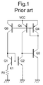
- Fig. 1 shows the bipolar reference current circuit described in Japanese Patent Application Laid-Open No. 191629/1984, which is generally called a proportional to absolute temperature (PTAT) current source circuit because it outputs a current proportional to temperature.
- PTAT proportional to absolute temperature
- the PTAT current source circuit shown in Fig. 1 is adapted to prevent appearance of the effect of Early voltage. It is because collectors of respective transistors Q5 and Q6 are connected to bases of respective transistors Q3 and Q4 and, by setting currents flowing to the transistors Q3 and Q4 equal to each other, base bias voltages of the transistors Q3 and Q4 can be set equal to each other, and thus collector voltages of the transistors Q5 and Q6 are set equal to each other.
- the transistors Q2 and Q3 are set as unit transistors, and the emitter area ratio of a transistor Q1 is set to be K 1 times (K 1 >1) as large as that of the unit transistor.
- I C KI S exp (V BE / V T )
- q denotes a unit electron charge; k the Boltzmann constant; T absolute temperature; and K the emitter area ratio with respect to the unit transistor.
- the transistor Q3 drives the transistor Q4.
- mirror current I C2 is exponentially increased with respect to an increase of reference current I C1 .
- I C1 >I C2 is established with I p >I C1
- I C1 ⁇ I C2 is established with I p ⁇ I C1 .
- Ip+ ⁇ I ⁇ I>0
- collector voltages of the transistors Q5 and Q6 are fixed with these base bias voltages of the transistors Q2 and Q3, and equally set, no effects of Early voltages of the transistors Q1 and Q2 appear. Since no changes occur in a desired current mirror ratio even if the collector voltages of the transistors Q5 and Q6 are changed to cause the appearance of effects of Early voltages, a highly accurate current output having only small changes with respect to fluctuation in a power supply voltage is obtained.
- a reference voltage circuit having no temperature characteristics because of cancellation, and adapted to output a reference voltage of 1.2 V or lower has conventionally been available.
- An example is described in IEEE Journal of Solid-State Circuits, Vol. 32, No. 11, pp.1790 to 1806, Nov. 1997.
- FIG. 3 shows the reference voltage circuit described in IEEE Journal of Solid-State Circuits, Vol. 32, No. 11, pp. 1790 to 1806, Nov. 1997.
- a current proportional to temperature is generally outputted.
- an output current of a reference current circuit called a proportional to absolute temperature (PTAT) current source circuit is supplied into an output circuit, where it is converted into a voltage and set as a reference voltage.
- PTAT proportional to absolute temperature
- q denotes a unit electron charge; k Boltzmann constant; T absolute temperature; and K the emitter area ratio with respect to the unit transistor.
- a transistor M6 constituting a current mirror circuit with the transistors M4 and M5
- Drain current I D6 of the transistor M6 is converted into a voltage by the output circuit, and set as a reference voltage V REF .
- a coefficient term R 3 /(R 2 +R 3 ) of equation (19) is 0 ⁇ R 3 /(R 2 +R 3 ) ⁇ 1.
- V BE3 has a negative temperature characteristic of about -1.9 mV/°C
- the thermal voltage V T has a positive temperature characteristic of 0.0853 mV/°C. Accordingly, in order to prevent a reference voltage V REF to be outputted from having no temperature characteristics, temperature characteristics cancel each other between a voltage having a positive temperature characteristic and a voltage having a negative temperature characteristic.
- the value of (R 2 /R 1 )1n(K1) is 22.3, and the voltage value of (R 2 /R 1 )V T 1n(K1) is 0.57 V.
- V BE3 is 0.7 V
- the reference voltage V REF can be set to a value equal to 1.27 V or lower, e.g., 1.0 V.
- a non-linear current mirror circuit was used for the PTAT current source circuit, and prevention of appearance of the effect of Early voltage was achieved only by using the foregoing Widlar current mirror circuit or the Widlar current mirror circuit described in the other embodiment of Japanese Patent Application Laid-Open No. 191629/1984 as the non-linear current mirror circuit.
- Reference current circuits are usually used for bias currents in circuits of an LSI including an analog LSI, a digital LSI such as a memory, and many other kinds of an LSI.
- the reference current circuit for outputting a current proportional to temperature is generally called a PTAT current source circuit.
- a reference current circuit having an optional temperature characteristic is requested.
- a reference voltage circuit can be easily realized by converting an output current of a reference current circuit having no temperature characteristics into a voltage through a resistor, and an output voltage of an optional value can be obtained.
- the reference voltage circuit having no temperature characteristics is generally called a band gap reference voltage circuit, and its output voltage is near a band gap voltage 1.205 V of silicon (Si) at absolute zero.
- Si silicon
- the reference voltage circuit for outputting a reference voltage having no temperature characteristics since an operation amplifier is used for a feedback circuit of the PTAT current source circuit, operation is difficult by a low power supply voltage. That is, reference voltage circuits are usually used for bias currents in circuits of an LSI including an analog LSI, a digital LSI such as memory devices, and many other kinds of an LSI.
- the reference voltage circuit for outputting a voltage having no temperature characteristics is generally called a band gap reference voltage circuit. Its output voltage is near a band gap voltage 1.205 V of silicon (Si) at absolute zero.
- An object of the present invention is to provide a reference current circuit operated from a low power supply voltage of about 1 V, and adapted to output a current having a positive or optional temperature characteristic.
- the object of the present invention is to provide a PTAT current source circuit using the Nagata current mirror circuit, and adapted to prevent the appearance of an effect of an early voltage, and a reference current circuit having an optional temperature characteristic by using the PTAT current source circuit thus obtained.
- Another object of the present invention is to provide a reference voltage circuit operated from a low power supply voltage of about 0.9 V, and adapted to output a voltage having no temperature characteristics by simple and small circuitry.
- a reference current circuit comprising: a power supply line; a ground line; a current mirror circuit installed between the power supply line and the ground line; and a third transistor connected between between the power supply line and the ground line.
- the current mirror circuit includes a first resistor having one end connected to a first node, and the other end connected to a second node, a first transistor connected between the second node and the ground line, and having a control terminal connected to the first node, and a second transistor connected between a third node and the ground line, and having a control terminal connected to the second node, and the third transistor has a control terminal connected to the third node, drives the current mirror circuit for setting a current source for driving the first and second transistors as a mirror current, and constitutes a negative feedback current loop.
- a reference current circuit comprising: a power supply line; a ground line; a current mirror circuit installed between the power supply line and the ground line; and a third transistor connected between the power supply line and the ground line.
- the current mirror circuit includes a first resistor having one end connected to a second node, and the other end connected to the ground line, a first transistor connected between the first and second nodes, and having a control terminal connected to the first node, and a third node, and a second transistor connected between a fourth node and the ground line, and having a control terminal connected to the third node, and the third transistor has a control terminal connected to the third node, drives the current mirror circuit for setting a current source for driving the first and second transistors as a mirror current, and constitutes a negative feedback current loop.
- a reference current circuit comprising: a power supply line; a ground line; a current mirror circuit installed between the power supply line and the ground line; and a third transistor connected between the power supply line and the ground line
- the current mirror circuit includes a first resistor having one end connected to a fourth node, and the other end connected to the ground line, a first transistor connected between a first node and the ground line, and having a control terminal connected to each of the first node and a second node, and a second transistor connected between a third node and the fourth node, and having a control terminal connected to the second node
- the third transistor has a control terminal connected to the third node, drives the current mirror circuit for setting a current source for driving the first and second transistors as a mirror current, and constitutes a negative feedback current loop.
- a reference current circuit comprising: a power supply line; a ground line; a current mirror circuit installed between the power supply line and the ground line; and a third transistor connected between the power supply line and the ground line; and second and third resistors.
- the current mirror circuit includes a first resistor having one end connected to a second node, and the other end connected to the ground line, a first transistor connected between the first and second nodes, and having a control terminal connected to the first node and a third node, and a second transistor connected between a fourth node and the ground line, and having a control terminal connected to the third node, the second resistor has one end connected to the first node, and the other end connected to the ground line, the third resistor has one end connected to the fourth node, and the other end connected to the ground line, and the third transistor has a control terminal connected to the fourth node, drives the current mirror circuit for setting a current source for driving the first and second transistors as a mirror current, and constitutes a negative feedback current loop.
- a reference current circuit comprising: a power supply line; a ground line; a current mirror circuit installed between the power supply line and the ground line; and a third transistor connected between the power supply line and the ground line; and second and third resistors.
- the current mirror circuit includes a first resistor having one end connected to a first node, and the other end connected to a second node, a first transistor connected between the second node and the ground line, and having a control terminal connected to the first node and a third node, and a second transistor connected between the third node and the ground line, and having a control terminal connected to the second node, the second resistor has one end connected to the first node, and the other end connected to the ground line, the third resistor has one end connected to the third node, and the other end connected to the ground line, and the third transistor has a control terminal connected to the third node, drives the current mirror circuit for setting a current source for driving the first and second transistors as a mirror current, and constitutes a negative feedback current loop.
- a reference current circuit comprising: a power supply line; a ground line; a current mirror circuit installed between the power supply line and the ground line; a third transistor connected between the power supply line and the ground line; and second and third resistors.
- the current mirror circuit includes a first resistor having one end connected to a fourth node, and the other end connected to a second node, a first transistor connected between a first node and the ground line, and having a control terminal connected to the first and second nodes, and a second transistor connected between a third node and the fourth node, and having a control terminal connected to the second node, the second resistor has one end connected to the first node, and the other end connected to the ground line, the third resistor has one end connected to the third node, and the other end connected to the ground line, and the third transistor has a control terminal connected to the third node, drives the current mirror circuit for setting a current source for driving the first and second transistors as a mirror current, and constitutes a negative feedback current loop.
- reference current circuit of the present invention may employ various suitable application forms described below.
- a fifth resistor which includes a plurality of resistors connected in series.
- current from the third transistor is set to be substantially inversely proportional to temperature
- a current mirror circuit current flowing to the transistor of the current mirror circuit and the current of the third transistor are weighted and added, and an output current having a fixed temperature characteristic is obtained.
- a reference voltage circuit comprising: a power supply line; a ground line; a current mirror circuit installed between the power supply line and the ground line; and a third transistor connected between the power supply line and the ground line.
- the current mirror circuit includes a first resistor having one end connected to a second node, and the other end connected to the ground line, a first transistor connected between a first node and the second node, and having a control terminal connected to the first node and a third node, and a second transistor connected between a fourth node and the ground line, and having a control terminal connected to the third node, the reference voltage circuit being self-biased to constitute a reference current circuit, and including a second resistor having one end connected to a fourth node, and the other end connected to a fifth node, the third transistor connected between the fifth node and the ground line, and having a control terminal connected to the fifth node, and a third resistor having one end connected to the fourth node, and the other end connected to the ground line, and an output voltage being obtained by supplying an output current of the reference current circuit to paths of the third transistor and the third resistor through the second resistor.
- a reference voltage circuit comprising: a power supply line; a ground line; a current mirror circuit installed between the power supply line and the ground line; and a third transistor connected between the power supply line and the ground line.
- the current mirror circuit includes a first resistor having one end connected to a first node, and the other end connected to a second node, a first transistor connected between the second node and the ground line, and having a control terminal connected to the first node, and a second transistor connected between a third node and the ground line, and having a control terminal connected to the second node, the reference voltage circuit being self-biased to constitute a reference current circuit, and including a second resistor having one end connected to a fourth node, and the other end connected to a fifth node, the third transistor connected between the fifth node and the ground line, and having a control terminal connected to the fifth node, and a third resistor having one end connected to the fourth node, and the other end connected to the ground line, and an output voltage being obtained by supplying an output current of the reference current circuit to paths of the third transistor and the third resistor through the second resistor.
- a reference voltage circuit comprising: a power supply line; a ground line; a current mirror circuit installed between the power supply line and the ground line; and a third transistor connected between the power supply line and the ground line.
- the current mirror circuit includes a first resistor having one end connected to a fourth node, and the other end connected to the ground line, a first transistor connected between a first node and the second node, and having a control terminal connected to the first node and a second node, and a second transistor connected between a third node and the fourth node, and having a control terminal connected to the second node, the reference voltage circuit being self-biased to constitute a reference current circuit, and including a second resistor having one end connected to the fourth node, and the other end connected to a fifth node, the third transistor connected between the fifth node and the ground line, and having a control terminal connected to the fifth node, and a third resistor having one end connected to the fourth node, and the other end connected to the ground line, and an output voltage being obtained by supplying an output current of the reference current circuit to paths of the third transistor and the third resistor through the second resistor.
- a reference voltage circuit comprising: a power supply line; a ground line; a current mirror circuit installed between the power supply line and the ground line; and a third transistor connected between the power supply line and the ground line.
- the current mirror circuit includes a first resistor having one end connected to a second node, and the other end connected to the ground line, a first transistor connected between a first node and the second node, and having a control terminal connected to the first node and a third node, and a second transistor connected between a fourth node and the ground line, and having a control terminal connected to the third node, the third transistor connected between a fifth node and the ground line drives a reference transistor of the current mirror circuit for setting a current source for driving the first and second transistors as a mirror current, and constitutes a negative feedback current loop, and the reference voltage circuit including a second resistor having one end connected to the fourth node, and the other end connected to the fifth node, the third transistor connected between the fifth node and the ground line, and having a control terminal connected to the fifth node, and a third resistor having one end connected to the fourth node, and the other end connected-to the ground line, and an output voltage being obtained by supplying an output current proportional
- a reference voltage circuit comprising: a power supply line; a ground line; a current mirror circuit installed between the power supply line and the ground line; and a third transistor connected between the power supply line and the ground line.
- the current mirror circuit includes a first resistor having one end connected to a first node, and the other end connected to a second node, a first transistor connected between the second node and the ground line, and having a control terminal connected to the first node, and a second transistor connected between a third node and the ground line, and having a control terminal connected to the second node, and the third transistor connected between a fifth node and the ground line wire drives a reference transistor of the current mirror circuit for setting a current source for driving the first and second transistors as a mirror current, and constitutes a negative feedback current loop, the reference voltage circuit including a second resistor having one end connected to a fourth node, and the other end connected to the fifth node, the third transistor connected between the fifth node and the ground line, and having a control terminal connected to the fifth node, and a third resistor having one end connected to the fourth node, and the other end connected to the ground line, and an output voltage being obtained by supplying an output current proportional to a current of
- a reference voltage circuit comprising: a power supply line; a ground line; a current mirror circuit installed between the power supply line and the ground line; and a third transistor connected between the power supply line and the ground line.
- the current mirror circuit includes a first resistor having one end connected to a fourth node, and the other end connected to the ground line, a first transistor connected between a first node and the ground line, and having a control terminal connected to the first node and a second node, and a second transistor connected between a third node and the fourth node, and having a control terminal connected to the second node, and the third transistor connected between a fifth node and the ground line drives a reference transistor of the current mirror circuit for setting a current source for driving the first and second transistors as a mirror current, and constitutes a negative feedback current loop, the reference voltage circuit including a second resistor having one end connected to the fourth node, and the other end connected to the fifth node, the third transistor connected between the fifth node and the ground line, and having a control terminal connected to the fifth node, and a third resistor having one end connected to the fourth node, and the other end connected to the ground line, and an output voltage being obtained by supplying an output current proportional to
- the reference voltage circuit of the present invention may employ various suitable application forms described below.
- an output circuit composed of a fourth transistor having a control terminal connected through the second resistor to a current input terminal, and a current output terminal connected to the ground line, and the third resistor having one terminal connected to the ground line, and the current mirror circuit for driving the output circuit are series-connected by n stages, and n output voltages are outputted.
- an output circuit composed of a fourth transistor having a control terminal connected through the second resistor to a current input terminal, and a current output terminal connected to the ground line, and the third resistor having one terminal connected to the ground line is series-connected by n stages, and n output voltages are outputted by sharing a circuit current.
- the first to third transistors are bipolar transistors.
- the first to third transistors are field-effect transistors.
- the first to third transistors are bipolar transistors.
- the first to third transistors are field-effect transistors.
- self-biasing sets a collector (or drain ) current of each to be a current I PTAT proportional, or substantially proportional to a temperature.
- the voltage between the base and the emitter (or between the gate and the source) has a negative temperature characteristic.
- a current proportional to the voltage between the base and the emitter (or between the gate and the source) is set to be a current I IPTAT substantially inversely proportional to the temperature.
- a reference voltage circuit for outputting an optional voltage value having a fixed temperature characteristic can be provided.
- Fig. 1 is a view showing an example of a conventional highly accurate bipolar PTAT reference current circuit, using a highly accurate bipolar self-biased inverse Widlar reference current circuit.
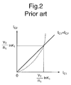
- Fig. 2 is a view showing an input/output characteristic of the conventional bipolar inverse Widlar current mirror circuit.
- Fig. 3 is a view showing a conventional reference voltage circuit using an operation amplifier.
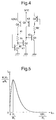
- Fig. 4 is a view showing an example of a reference current circuit according to a first embodiment of the present invention, using a highly accurate bipolar self-biased Nagata reference current circuit.
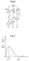
- Fig. 5 is a view showing an input/output characteristic of the bipolar Nagata current mirror circuit.
- Fig. 6 is a view showing an example of the reference current circuit of the first embodiment using a highly accurate CMOS self-biased Nagata reference current circuit.
- Fig. 7 is a view showing an input/output characteristic of the MOS Nagata current mirror circuit.
- Fig. 8 is a view showing a temperature characteristic of an inverse number 1/ ⁇ of a transconductance parameter.
- Fig. 9 is a view showing an example of a reference current circuit according to a second embodiment using a highly accurate CMOS self-biased inverse Widlar reference current circuit.
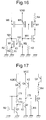
- Fig. 10 is a view showing an input/output characteristic of the MOS inverse Widlar current mirror circuit.
- Fig. 11 is a view showing an example of a reference current circuit according to a third embodiment using a highly accurate bipolar self-biased Widlar reference current circuit.
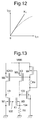
- Fig. 12 is a view showing an input/output characteristic of the bipolar Widlar current mirror circuit.
- Fig. 13 is a view showing an example of the reference current circuit of the third embodiment using a highly accurate CMOS self-biased Widlar reference current circuit.
- Fig. 14 is a view showing an input/output characteristic of the MOS Widlar current mirror circuit.
- Fig. 15 is a view showing an example of a reference current circuit according to a fourth embodiment using a bipolar inverse Widlar reference current circuit.
- Fig. 16 is a view showing an example of the reference current circuit of the fourth embodiment using a CMOS inverse Widlar reference current circuit.
- Fig. 17 is a view showing an example of a reference current circuit according to a fifth embodiment using a bipolar Nagata reference current circuit.
- Fig. 18 is a view showing an example of the reference current circuit of the fifth embodiment using a CMOS Nagata reference current circuit.
- Fig. 19 is a view showing an example of a reference current circuit according to a sixth embodiment using a bipolar Widlar reference current circuit.
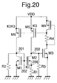
- Fig. 20 is a view showing an example of the reference current circuit of the sixth embodiment using a CMOS Widlar reference current circuit.
- Fig. 21 is a view showing an example of a reference voltage circuit according to a seventh embodiment using a bipolar self-biased inverse Widlar reference current circuit.
- Fig. 22 is a view showing an example of the reference voltage circuit of the seventh embodiment using a CMOS self-biased inverse Widlar reference current circuit.
- Fig. 23 is a view showing an example of a reference voltage circuit according to an eighth embodiment using a bipolar self-biased Nagata Widlar reference current circuit.
- Fig. 24 is a view showing an example of the reference voltage circuit of the eight embodiment using a CMOS self-biased Nagata Widlar reference current circuit.
- Fig. 25 is a view showing an example of a reference voltage circuit according to a ninth embodiment using a bipolar self-biased Widlar reference current circuit.
- Fig. 26 is a view showing an example of the reference voltage circuit of the ninth embodiment using a CMOS self-biased Widlar reference current circuit.
- Fig. 27 is a view showing an example of a reference voltage circuit according to a tenth embodiment using a bipolar self-biased inverse Widlar reference current circuit.
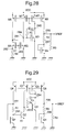
- Fig. 28 is a view showing an example of the reference voltage circuit of the tenth embodiment using a CMOS self-biased inverse Widlar reference current circuit.
- Fig. 29 is a view showing an example of a reference voltage circuit according to an eleventh embodiment using a bipolar self-biased Nagata Widlar reference current circuit.
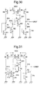
- Fig. 30 is a view showing an example of the reference voltage circuit of the eleventh embodiment using a CMOS self-biased Nagata Widlar reference current circuit.
- Fig. 31 is a view showing an example of a reference voltage circuit according to a twelfth embodiment using a bipolar self-biased Widlar reference current circuit.
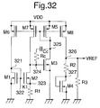
- Fig. 32 is a view showing an example of the reference voltage circuit of the twelfth embodiment using a CMOS self-biased Widlar reference current circuit.
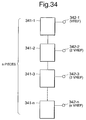
- Fig. 33 is a view showing an example of a circuit, where any one of the reference voltage circuits of the seventh to twelfth embodiments is series-connected.
- Fig. 34 is a view showing an example of a circuit, where any one of the reference voltage circuits of the seventh to twelfth embodiments is series-connected.
- the reference current circuit of the first embodiment of the present invention is shown constructed in a manner that transistors Q1 and Q2, and a resistor R1 constitute the bipolar Nagata current mirror circuit, and transistors Q4, Q5, (Q6), and a resistor R4 constitute the bipolar Nagata current mirror circuit.
- transistors Q5 and Q6 the transistors Q1 and Q2, and the resistor R1 constitute the bipolar self-biased Nagata reference current circuit.
- a circuit constant is set such that when a current of transistor Q3 to be driven is increased, currents flowing to transistors Q5 and Q6 can be reduced.
- a negative feedback current loop is formed in the circuit, enabling the circuit to be stably operated.
- Fig. 5 shows an input/output characteristic of the bipolar Nagata current mirror circuit (Fig. 4) constituted of transistors Q1 and Q2 and resistor R1.
- the abscissa indicates an input current I C1
- the ordinate indicates an output current I C2 .
- a feature of the bipolar Nagata current mirror circuit is that there are a region where the output current (mirror current) I C2 is monotonously increased with respect to the input current (reference current) I C1 , a peak point, and a region where the output current (mirror current) I C2 is monotonously reduced with respect to the input current (reference current) I C1 .
- the transistor Q4 constitutes the bipolar Nagata current mirror circuit with transistors Q5 and Q6 and resistor R4, which is operated in the region where the output current (mirror current) is monotonously reduced with respect to the input current (reference current).
- the transistors Q1 and Q2 are respectively driven by transistors Q6 and Q5.
- transistor Q4 is a unit transistor
- the emitter area ratio of the transistor Q5 is K 3 times as large as that of the unit transistor
- the emitter area ratios K1, K2 and K3, and values of the resistors R1 and R4 are set.
- base bias voltages of the transistors Q1 and Q3 are substantially equal to each other, fixing and setting collector voltages of the transistors Q1 and Q3 to be equal to each other.
- no effects of Early voltages of the transistors Q1 and Q2 appear, and no changes occur in a desired current mirror ratio even if the collector voltages of the transistors Q5 and Q6 are changed to cause the appearance of effects of Early voltages, making it possible to obtain a highly accurate current output having only a small change with respect to fluctuation in a power supply voltage.
- the collector voltages of the transistors Q1 and Q2 are fixed by at least the base bias voltages of the transistors Q1 and Q3, the fluctuation extent is limited, and thus almost no effects of Early voltages (base width modulation) of the transistors Q1 and Q2 appear.
- Fig. 6 shows the reference current circuit of the first embodiment, specifically a CMOS reference current circuit of another embodiment.
- transistors M1 and M2 and a resistor R1 constitute the Nagata current mirror circuit and, similarly, transistors M4, and M5 (M6), and a resistor R4 constitute the Nagata current mirror circuit.
- transistors M5 and M6 constituting a current source
- the transistors M1 and M2 and the resistor R1 constitute the self-biased Nagata reference current circuit.
- the MOS Nagata reference current circuit constituted of the transistors M4 and M5 (M6), and the resistor R4 has a circuit constant set such that when a current of a transistor M3 to be driven is increased, currents flowing to the transistors M5 and M6 can be reduced.
- a negative feedback current loop is formed, and the circuit is stably operated.
- a positive feedback current loop is formed in the circuit, and thus the circuit is not operated.
- the transistor M1 is a unit transistor, and ratio (W/L) of gate width W to gate length L of the transistor M2 is K 1 times (K 1 >1) as large as that of the unit transistor.
- ⁇ denotes the effective mobility of a carrier
- C OX the gate oxide capacitance per unit area
- W and L respectively the width and length of the gate.
- Fig. 7 shows an input/output characteristic of the MOS Nagata current mirror circuit constituted of transistors M1 and M2 and resistor R1.
- the abscissa indicates input current I D1
- the ordinate indicates output current I D2 .
- a feature of the MOS Nagata current mirror circuit is that as in the case of the bipolar Nagata current mirror circuit, there are a region where the output current (mirror current) I D2 is monotonously increased with respect to the input current (reference current) I D1 , a peak point, and a region where the output current (mirror current) I D2 is monotonously reduced with respect to the input current (reference current) I D1 .
- I D2 K 1 /16R 1 2 ⁇ .
- transistor M3 drives transistor M4.
- the transistor M4 constitutes the MOS Nagata current mirror circuit with transistors M5 and M6 and resistor R4, which is operated in the region where the output current (mirror current) is monotonously reduced with respect to the input current (reference current).
- the transistors M1 and M2 are respectively driven by the transistors M6 and M5.
- the MOS self-biased Nagata current circuit is provided.
- K 1 and K 2 denote constants having no temperature characteristics.
- Fig. 8 showsthe calculated value of a temperature characteristic of 1/ ⁇ (inverse number of the transconductance parameter) in the circuit of Fig. 6.
- the temperature characteristic of 1/ ⁇ is 5000 ppm/°C at a normal temperature. This is 1.5 times as large as that of a temperature characteristic 3333 ppm/°C of the thermal voltage V T of the bipolar transistor.
- K 1 and K 2 denote constants having no temperature characteristics.
- the temperature characteristic of 1/ ⁇ is substantially proportional to a temperature, being 5000 ppm/°C at the normal temperature. This is 1.5 times as large as that of the temperature characteristic 3333 ppm/°C of the thermal voltage V T of the bipolar transistor. If the temperature characteristic of the resistor R2 is equal to or lower than 5000 ppm/°C, being a primary characteristic with respect to temperature, the drain current I D1 has a positive temperature characteristic, the output current I 0 of the reference current circuit outputted through the current mirror circuit being proportional to the temperature, realizing a PTAT current source circuit.
- transistor size ratios (ratio (W/L) of gate width W between gate length L (W/L)) K1, K2 and K3 are set, and values of the resistors R1 and R4 are set.
- gate voltages of transistors M1 and M3 can be set substantially equal to each other, fixing and setting drain voltages of the transistors M1 and M3 to be equal to each other.
- Fig. 9 shows a reference current circuit of the second embodiment of the invention with transistors M1 and M2, and resistor R1 constituting the MOS inverse Widlar current mirror circuit.
- transistors M1 and M2 As described above with reference to prior art, a negative feedback current loop is formed, and the circuit is stably operated at a set operation point.
- the MOS inverse Widlar current mirror circuit is self-biased to realize a CMOS reference current circuit.
- T ransistor M3 drives transistor M4, and transistor M4 constitutes a current mirror circuit with transistors M5 and M6.
- Transistors M1 and M2 are respectively driven by the transistors M6 and M5.
- I D1 K 2 R 2 1 ⁇ 1 - 1 K 1 K 2
- K 1 and K 2 denote constants having no temperature characteristics.
- mobility ⁇ has a temperature characteristic in the MOS transistor, temperature dependence of transconductance parameter ⁇ is represented byte the equation (31), and output current I REF of the CMOS reference current circuit is obtained by the following equation (44):
- K1 and K2 denote constants having no temperature characteristics and, as described above,the temperature characteristic of 1/ ⁇ is substantially proportional to a temperature, being 5000 ppm/°C at normal temperature.
- the output current I 0 of the reference current circuit outputted through the current mirror circuit is proportional to the temperature, realizing a PTAT current source circuit.
- K 2 1
- transistors M2 to M6 as unit transistors, gate voltages of the transistors M1 and M3 can be set equal to each other, and drain voltages of the transistors M5 and M6 are fixed and set equal to each other.
- Fig. 11 shows the reference current circuit of the third embodiment, in which transistors Q1 and Q2 and a resistor R1 constitute the bipolar Widlar current mirror circuit and, similarly, transistors Q4, Q5, (Q6), and a resistor R4 constitute the bipolar Nagata current mirror circuit.
- the transistors Q5 and Q6 constituting a current source, transistors Q1 and Q2, and resistor R1 constitute the bipolar self-biased Widlar reference current circuit.
- a circuit constant is set such that when the current of the transistor Q3 to be driven is increased, current flowing to the transistors Q5 and Q6 can be reduced.
- a negative feedback current loop is formed, enabling the circuit to be stably operated.
- a positive feedback current loop is formed in the circuit, and thus the circuit is not operated.
- transistor Q3 drives transistor Q4, which constitutes the bipolar Nagata current mirror circuit with transistors Q5 and Q6 and the resistor R4, which is operated in a region where the output current (mirror current) is monotonously reduced with respect to the input current (reference current).
- Transistors Q1 and Q2 are respectively driven by the transistors Q6 and Q5.
- transistor Q4 is a unit transistor
- the emitter area ratio of the transistor Q5 is K 3 times as large as that of the unit transistor
- the emitter area ratio of the transistor Q6 is K 2 K 3 times as large as that of the unit transistor.
- the emitter area ratios K1, K2 and K3, and values of the resistors R1 and R4 are set.
- base bias voltages of the transistors Q1 and Q3 are substantially equal to each other, fixing and setting collector voltages of transistors Q1 and Q3 to be equal to each other.
- no effects of Early voltages of the transistors Q1 and Q2 appear, and no changes occur the desired current mirror ratio even if the collector voltages of the transistors Q5 and Q6 are changed to cause appearance of effects of Early voltages, making it possible to obtain a highly accurate current output having only a small change with respect to fluctuation in a power supply voltage.
- the collector voltages of the transistors Q1 and Q2 are fixed by at least the base bias voltages of transistors Q1 and Q3, the fluctuation extent is limited, and thus almost no effects of Early voltages of transistors Q1 and Q2 appear.
- Fig. 13 shows the reference current circuit of the third embodiment, in which transistors M1 and M2 and a resistor R1 constitute the MOS Widlar current mirror circuit and, similarly, transistors M4, and M5 (M6), and a resistor R4 constitute the MOS Nagata current mirror circuit.
- transistors M5 and M6 constituting a current source
- transistors M1 and M2 and resistor R1 constitute the CMOS self-biased Widlar reference current circuit.
- the MOS Nagata reference current circuit constituted of the transistors M4 and M5 (M6), and the resistor R4 has a circuit constant set such that whenthe current of a transistor M3 to be driven is increased, currents flowing to the transistors M5 and M6 can be reduced.
- a negative feedback current loop is formed, and the circuit is stably operated.
- a positive feedback current loop is formed in the circuit, and thus the circuit is not operated.
- Fig. 14 shows an input/output characteristic of the MOS Widlar current mirror circuit constituted of the transistors M1 and M2 and resistor R1.
- the transistor M1 is a unit transistor, and ratio (W/L) of gate width W to gate length L of transistor M2 is K 1 times (K 1 >1) as large as that of the unit transistor.
- ratio (W/L) of gate width W to gate length L of transistor M2 is K 1 times (K 1 >1) as large as that of the unit transistor.
- transistor M3 drives transistor M4.
- the transistor M4 constitutes the MOS Nagata current mirror circuit with transistors M5 and M6 and resistor R4 which is operated in a region where the output current (mirror current) is monotonously reduced with respect to the input current (reference current).
- the transistors M1 and M2 are respectively driven by the transistors M6 and M5.
- the MOS self-biased Widlar current circuit is provided.
- K 1 and K 2 denote constants having no temperature characteristics.
- the mobility ⁇ has a temperature characteristic in the MOS transistor
- the temperature dependence of the transconductance parameter ⁇ is represented by equation (31)
- the output current I REF of the CMOS reference current circuit is represented by the following equation (59) :
- K 1 and K 2 denote constants having no temperature characteristics.
- the temperature characteristic of 1/ ⁇ is substantially proportional to the temperature, being 5000 ppm/°C at the normal temperature.
- the drain current I D1 has a positive temperature characteristic
- the output current I 0 of the reference current circuit outputted through the current mirror circuit is proportional to the temperature, realizing a PTAT current source circuit.
- transistor size ratios (ratio (W/L) of gate width W between gate length L ) K1, K2 and K3 are set, and values of the resistors R1 and R4 are set.
- gate voltages of the transistors M1 and M3 can be set substantially equal to each other, fixing and setting drain voltages of the transistors M1 and M2 to be equal to each other.
- the reference current circuits for outputting currents having positive temperature characteristics have been described.
- Each of the foregoing circuits is constructed such that the collector (drain) voltages of the two output transistors constituting the current mirror circuit can be equal, or substantially equal to each other.
- the temperature characteristics of the collector (or drain) voltages of at least the two output transistors constituting the current mirror circuit are negative.
- a current I IPTAT having a negative temperature characteristic is obtained, and this current I IPTAT and a current I PTAT having a positive temperature characteristic obtained from the PTAT current mirror source are weighted and added.
- a reference current circuit for outputting a current having an optional temperature characteristic.
- Fig. 15 shows a reference current circuit according to a fourth embodiment specifically of a bipolar reference current circuit, which outputs a current having an optional temperature characteristic.
- the reference current circuit is shown to be constructed in a manner that transistors Q1 and Q2, and a resistor R1 constitute the bipolar inverse Widlar current mirror circuit, and transistors Q4, Q5, (Q6), and a resistor R4 constitute the bipolar inverse Widlar current mirror circuit. If the ratio of currents flowing to resistors R2 and R3 is equal to that of currents of the current mirror circuit constituted of transistors Q5 and Q6, transistors Q1, Q2 (Q3), Q5 and Q6, and resistor R1 constitute the bipolar self-biased inverse Widlar reference current circuit.
- the ratio of resistance values of resistors R2 and R3 may be set inverse to the current ratio of the current mirror circuit.
- Transistors Q4, Q5, (Q6) and resistor R4 constitute the bipolar inverse Widlar current mirror circuit, and transistors Q5 and Q6 are unit transistors.
- the emitter area ratio of transistor Q4 is K 3 times as large as that of the unit transistor.
- ⁇ V BE is proportional to temperature.
- the output current I REF of the bipolar reference current circuit is obtained by the following equation (66): That is, the output current I REF of the bipolar reference current circuit is represented by an equation of weighting and adding a base-emitter bias voltage V BE having a negative temperature characteristic and ⁇ V BE having a positive temperature characteristic. Accordingly, by changing weight factors, temperature characteristics of two reference voltages can be optionally set as described above. Specifically, the emitter area ratio or current mirror ratio and each resistance ratio may be set. For example, by converting the output current I REF of the bipolar reference current circuit into a voltage by the resistor R5, an output voltage V REF obtained is represented by the following equation (67) :
- the thermal voltage V T has a positive temperature characteristic of 3333 ppm/°C
- the base-emitter bias voltages V BE2 and V BE3 of the transistors Q2 and Q3 have negative temperature characteristics of about -1.9 mV/°C.
- the resistance ratios (R 5 /R 1 ) and (R 5 /R 3 ) are zero because of cancellation of temperature characteristics, and ln(K 1 K 2 ) has no temperature characteristics.
- the output voltage V REF obtained by converting the output current of the bipolar reference current circuit into a voltage through the resistor is decided by the positive temperature characteristic, 3333 ppm/°C, of the thermal voltage V T , and the negative temperature characteristic, about -1.9 mV/°C, of the base-emitter bias voltage V BE2 of the transistor Q2.
- the output voltage V REF having the temperature characteristic of zero thus obtained can be set to an optional voltage value by optionally setting a ratio (R 5 /R 3 ) of the resistors R 5 and R 3 .
- Fig. 16 shows the reference current circuit of the fourth embodiment, specifically a circuit which outputs a current having an optional temperature characteristic.
- This circuit is shown to be constructed in a manner that transistors M1 and M2 and a resistor R1 constitute the MOS inverse Widlar current mirror circuit, and transistors M4, and M5 (M6), and a resistor R4 constitute the MOS inverse Widlar current mirror circuit. If the ratio of currents flowing to the resistors R2 and R3 is equal to that of currents flowing to the current mirror circuit constituted of transistors M5 and M6, transistors M1, and M2 (M3), M5 and M6, and resistor R1 constitute the MOS self-biased inverse Widlar reference current circuit.
- the ratio of resistance values of resistors R2 and R3 may be set inverse to the current ratio of the current mirror circuit.
- the transistor M2 is a unit transistor, and a ratio (W/L) of a gate width W/a gate length L of the transistor M1 is K 1 times (K 1 >1) as large as that of the unit transistor.
- output current I REF of the MOS reference voltage current is obtained by the following equation (74):
- V GS2 I D2 ⁇ + V TH
- equation (76) the temperature characteristic of a threshold voltage V TH is represented by the following equation (77):
- V TH V TH0 - ⁇ (T - T 0 )
- ⁇ is about 2.3 mV/°C in a CMOS fabrication process of the MOS transistor having a low threshold voltage.
- the output current I REF of the MOS reference voltage circuit is represented by weighting and adding a term of the threshold voltage V TH having a negative temperature characteristic and a term of 1/ ⁇ having a positive temperature characteristic.
- V TH threshold voltage
- 1/ ⁇ 1/ ⁇ having a positive temperature characteristic
- the right side of the equation (78) is represented by weighting and adding of voltage values caused by inverse numbers of the threshold voltage V TH having a negative temperature characteristic and the transconductance parameter (mobility) having a positive temperature characteristic. Accordingly, by changing weight factors, it is possible to optionally setthe temperature characteristic of the output voltage V REF of the MOS reference voltage circuit as described above. Specifically, the (W/L)/(W/L) ratio, or current mirror ratio and resistance values, and each resistance ratio may be set.
- the temperature characteristic of 1/ ⁇ as an inverse number of the transconductance parameter ⁇ is substantially proportional to temperature, which is 5000 ppm/°C at a normal temperature.
- Threshold voltage V TH of the transistor M2 has a negative temperature characteristic of about -2.3 mV/°C.
- the temperature characteristics of the resistance ratios (R 5 /R 1 ) and (R 5 /R 3 ) are zero because of cancellation, and ⁇ K 1 has no temperature characteristics.
- the output voltage V REF of the MOS reference voltage circuit is decided by the positive temperature characteristic of 5000 ppm/°C, the negative temperature characteristic of the threshold voltage V TH of the transistor M2, and about -2.3 mV/°C.
- the voltage 1.16 V has no temperature characteristics.
- the temperature characteristic of the (R 5 /R 3 ) is zero because of cancellation, reference voltage V REF to be outputted has no temperature characteristics.
- V REF1 0.5V
- V REF2 1.0V
- V REF3 1.5 V
- V REF4 2.0 V
- Fig. 17 shows specifically an embodiment of a bipolar reference current circuit, which outputs a current having an optional temperature characteristic.
- This circuit is shown to be constructed in a manner that transistors Q1 and Q2, and a resistor R1 constitute the bipolar Nagata Widlar current mirror circuit, and the bipolar Nagata current mirror circuit constituted of transistors Q4, Q5, (Q6), and a resistor R4 has a circuit constant such that when a current of a transistor Q3 to be driven is increased, currents flowing to the transistors Q5 and Q6 can be reduced.
- a negative feedback current loop is provided in the circuit, enabling the circuit to be stably operated.
- the ratio of resistance values of resistors R2 and R3 may be set inverse to a current ratio of the current mirror circuit.
- the emitter area ratio of the transistor Q4 is K 3 times as large as that of the unit transistor.
- ⁇ V BE is proportional to temperature.
- An output current I REF of the bipolar reference voltage circuit is obtained by the following equation (87): That is, the output current I REF of the bipolar reference current circuit is represented by an equation of weighting and adding a base-emitter bias voltage V BE having a negative temperature characteristic and ⁇ V BE having a positive temperature characteristic. Accordingly, by changing weight factors, temperature characteristics of two reference voltages can be optionally set as described above. Specifically, the emitter area ratio or current mirror ratio and each resistance ratio may be set. For example, by converting the output current I REF of the bipolar reference current circuit into a voltage by the resistor R5, an output voltage V REF obtained is represented by the following equation (88):
- the thermal voltage V T has a positive temperature characteristic of 3333 ppm/°C
- the base-emitter bias voltages V BE2 and V BE3 of the transistors Q2 and Q3 have negative temperature characteristics of about -1.9 mV/°C.
- the resistance ratios (R 5 /R 1 ) and (R 5 /R 3 ) are zero because of cancellation of the temperature characteristics, and K 2 and ln(K 1 K 2 ) have no temperature characteristics.
- the output voltage V REF obtained by converting the output current of the bipolar reference current circuit into a voltage through the resistor is decided by the positive temperature characteristic, 3333 ppm/°C, of the thermal voltage V T , and the negative temperature characteristic, about -1.9 mV/°C, of the base-emitter bias voltage V BE2 of the transistor Q1.
- the output voltage V REF having the temperature characteristic of zero thus obtained can be set to an optional voltage value by optionally setting a ratio (R 5 /R 3 ) of the resistors R 5 and R 3 .
- a ratio (R 5 /R 3 ) of the resistors R 5 and R 3 In the setting of (R 5 /R 3 ) ⁇ 1, for example a case of setting 0.7 V is considered, operation is possible from about 0.9 V.
- a power supply voltage has allowance to increase voltage
- Fig. 18 shows specifically a CMOS reference current circuit, which outputs a current having an optional temperature characteristic.
- This fifth embodiment is shown to be constructed in a manner that transistors M1 and M2 and a resistor R1 constitute the MOS Nagata current mirror circuit, and the MOS Nagata current mirror circuit constituted of transistors M4, and M5 (M6), and a resistor R4 has a circuit constant set such that when a current of a transistor M3 to be driven is increased, currents flowing to the transistors M5 and M6 can be reduced.
- the ratio of resistance values of the resistors R2 and R3 may be set inverse tothe current ratio of the current mirror circuit.
- the transistor M2 is a unit transistor.
- the ratio of gate width W to gate length L (W/L) of transistor M1 is K 1 times (K 1 >1) as large as that of the unit transistor.
- Transistors M4 and M5 (M6), and resistor R4 constitute the MOS Nagata current mirror circuit.
- Transistors M5 and M6 are unit transistors,
- the ratio (W/L) of gate width W to gate length L of transistor M4 is K 3 times as large as that of the unit transistor.
- K 1 and K 2 denote the constants having no temperature characteristics.
- the mobility ⁇ has a temperature characteristic in the MOS transistor
- the temperature dependence of the transconductance parameter ⁇ is represented by the equation (34) and, as shown in Fig. 5, the temperature characteristic of 1/ ⁇ is substantially proportional to the temperature.
- the temperature characteristic of 1/ ⁇ is 5000 ppm/°C at the normal temperature. Therefore, it can be understood that if the temperature characteristic of the resistor R1 is equal to or lower than 5000 ppm/°C, drain current I D1 has a positive temperature characteristic.
- output current I REF of the MOS reference voltage current is obtained by the following equation (95) :
- V GS1 I D1 ⁇ + V TH
- equation (95) is rewritten into the following equation (97):
- the temperature characteristic of the threshold voltage V TH is represented by equation (77), where ⁇ is about 2.3 mV/°C in a CMOS fabrication process of the MOS transistor having a low threshold voltage.
- the output current I REF of the MOS reference voltage circuit is represented by weighting and adding a term of threshold voltage V TH having a negative temperature characteristic and a term of 1/ ⁇ having a positive temperature characteristic.
- V TH threshold voltage
- 1/ ⁇ 1/ ⁇ having a positive temperature characteristic
- Equation (98) is represented by weighting and adding of the voltage values caused by inverse numbers of the threshold voltage V TH having a negative temperature characteristic and the transconductance parameter (mobility) having a positive temperature characteristic. Accordingly, by changing weight factors, it is possible to optionally set a temperature characteristic of output voltage V REF of the MOS reference voltage circuit. Specifically, a (W/L)/(W/L) ratio, or a current mirror ratio and resistance values, and each resistance ratio may be set. In this case, a temperature characteristic of 1/ ⁇ as an inverse number of the transconductance parameter ⁇ is substantially proportional to the temperature, which is 5000 ppm/°C at a normal temperature.
- the threshold voltage V TH of the transistor M2 has a negative temperature characteristic of about -2.3 mV/°C.
- the temperature characteristics of the resistance ratios (R 5 /R 1 ) and (R 5 /R 3 ) are zero because of cancellation, and ⁇ K 1 has no temperature characteristics.
- the output voltage V REF of the MOS reference voltage circuit is decided by the positive temperature characteristic of 5000 ppm/°C, the negative temperature characteristic of the threshold voltage V TH of the transistor M2, and about -2.3 mV/°C.
- the voltage 1.16 V has no temperature characteristics.
- V REF1 0.5 V
- V REF2 1.0 V
- V REF3 1.5 V
- V REF4 2.0 V
- FIG. 19 shows a specific embodiment of a bipolar reference current circuit, which outputs a current having an optional temperature characteristic and is constructed in a manner that transistors Q1 and Q2, and a resistor R1 constitute the bipolar Widlar current mirror circuit, and the bipolar Nagata current mirror circuit constituted of transistors Q4, Q5, (Q6), and a resistor R4 has a circuit constant set such that if the current of a transistor Q3 to be driven is increased, currents flowing to transistors Q5 and Q6 can be reduced.
- a negative feedback current loop is provided in the circuit, which is stably operated.
- the ratio of resistance values of resistors R2 and R3 may be set inverse tothe current ratio of the current mirror circuit.
- Transistors Q4, Q5, (Q6) and resistor R4 constitute the bipolar Nagata current mirror circuit, and transistors Q5 and Q6 are unit transistors.
- the emitter area ratio of transistor Q4 is K 3 times as large as that of the unit transistor.
- ⁇ V BE is proportional to temperature.
- the output current I REF of the bipolar reference voltage circuit is obtained by the following equation (107) :
- the output current I REF of the bipolar reference current circuit is represented by an equation of weighting and adding the base-emitter bias voltage V BE having a negative temperature characteristic and ⁇ V BE having a positive temperature characteristic.
- the temperature characteristics of two reference voltages can be optionally set as described above.
- the emitter area ratio or current mirror ratio and each resistance ratio may be set.
- the output voltage V REF obtained is represented by the following equation (108):
- the thermal voltage V T has a positive temperature characteristic of 3333 ppm/°C
- the base-emitter bias voltages V BE2 and V BE3 of transistors Q2 and Q3 have negative temperature characteristics of about -1.9 mV/°C.
- the resistance ratios (R 5 /R 1 ) and (R 5 /R 3 ) are zero because of cancellation of temperature characteristics, and ln(K 1 K 2 ) has no temperature characteristics.
- the output voltage V REF obtained by converting the output current of the bipolar reference current circuit into a voltage through the resistor is decided by the positive temperature characteristic, 3333 ppm/°C, of the thermal voltage V T , and the negative temperature characteristic, about -1.9 mV/°C, of the base-emitter bias voltage V BE1 of the transistor Q1.
- the output voltage V REF having the temperature characteristic of zero thus obtained can be set to an optional voltage value by optionally setting a ratio (R 5 /R 3 ) of the resistors R 5 and R 3 .
- setting of (R 5 /R 3 ) ⁇ 1 for example 0.7 V being considered, operation is possible from about 0.9 V.
- a reference voltage having a temperature characteristic of zero at V REF >1.2 V is obtained.
- the resistor R 5 by setting the resistor R 5 to be R 5 >R 3 , and optionally providing the number (n-1) of taps in the resistor R 5 to set it as an output terminal, it is possible to obtain n reference voltages of optional different voltage values having no temperature characteristics.
- Fig. 20 shows a specific CMOS reference current circuit, which outputs a current having an optional temperature characteristic and is shown constructed in a manner that transistors M1 and M2 and a resistor R1 constitute the MOS Widlar current mirror circuit, and the MOS Nagata current mirror circuit constituted of transistors M4, and M5 (M6), and a resistor R4 has a circuit constant set such that when the current of a transistor M3 to be driven is increased, current flowing to the transistors M5 and M6 can be reduced. Accordingly, a negative feedback current loop is provided in the circuit, and the circuit is stably operated.
- the ratio of current flowing to the resistors R2 and R3 is equal to that of current flowing to the current mirror circuit constituted of transistors M5 and M6, transistors M1, and M2 (M3), M5 and M6, and resistor R1 constitute the MOS self-biased Nagata reference current circuit.
- the ratio of resistance values of resistors R2 and R3 may be set inverse to the current ratio of the current mirror circuit.
- the transistor M2 is a unit transistor
- the ratio (W/L) of gate width W to gate length L of transistor M1 is K 1 times (K 1 >1) as large as that of the unit transistor.
- transistor M1 and resistor R2 and transistor M2 and transistor R3 are driven by a current mirror having a mirror ratio of K 2 :1
- transistors M4 and M5 (M6), and resistor R4 constitute the MOS Nagata current mirror circuit
- transistor M4 is a unit transistor
- the ratio (W/L) of gate width W to gate length L of transistor M5 is K 3 times as large as that of the unit transistor.
- K 1 and K 2 denote constants having no temperature characteristics.
- mobility ⁇ has a temperature characteristic in the MOS transistor
- temperature dependence of the transconductance parameter ⁇ is represented by equation (34) and, as shown in Fig. 8, the temperature characteristic of 1/ ⁇ is substantially proportional to temperature.
- the temperature characteristic of 1/ ⁇ is 5000 ppm/°C at normal temperature. Therefore, it can be understood that if a temperature characteristic of resistor R1 is equal to or lower than 5000 ppm/°C, a drain current I D2 has a positive temperature characteristic.
- E quation (115) is rewritten into the following equation (117):
- the temperature characteristic of the threshold voltage V TH is represented by (77), where ⁇ is about 2.3 mV/°C in a CMOS fabrication process of the MOS transistor having a low threshold voltage.
- the output current I REF of the MOS reference voltage circuit is represented by weighting and adding a term of the threshold voltage V TH having a negative temperature characteristic and a term of 1/ ⁇ having a positive temperature characteristic.
- output voltage V REF is represented by the following equation (118):
- Equation (118) is represented by weighting and adding of voltage values caused by inverse numbers of the threshold voltage V TH having the negative temperature characteristic and the transconductance parameter (mobility) having the positive temperature characteristic. Accordingly, by changing weight factors, it is possible to optionally set a temperature characteristic of the output voltage V REF of the MOS reference voltage circuit as described above. Specifically, the (W/L)/(W/L) ratio, or current mirror ratio and resistance values, and each resistance ratio may be set.
- the temperature characteristic of 1/ ⁇ as an inverse number of the transconductance parameter ⁇ is substantially proportional to temperature, which is 5000 ppm/°C at normal temperature.
- the threshold voltage V TH of the transistor M2 has a negative temperature characteristic of about -2.3 mV/°C.
- the temperature characteristics of the resistance ratios (R 5 /R 1 ) and (R 5 /R 3 ) are zero because of cancellation, and ⁇ K 1 has no temperature characteristics.
- the output voltage V REF of the MOS reference voltage circuit is decided by the positive temperature characteristic of 5000 ppm/°C, the negative temperature characteristic of the threshold voltage V TH of the MOS reference voltage circuit, and about -2.3 mV/°C.
- the voltage 1.16 V has no temperature characteristics.
- the reference voltage V REF to be outputted has no temperature characteristics.
- V REF1 0.5 V
- V REF2 1.0 V
- V REF3 1.5 V
- V REF4 2.0 V
- Fig. 21 is a view showing an example of a reference voltage circuit according to a seventh embodiment of the present invention, specifically an embodiment of a bipolar reference voltage circuit, which is shown constructed in a manner that transistors Q1 and Q2, and a resistor R1 constitute the bipolar inverse Widlar current mirror circuit.
- the transistor Q5 constitutes the current mirror circuit with transistor Q4 (and Q6), which has a current mirror ratio of 1:1, and the transistors Q1 and Q2 are respectively driven by the transistors Q4 and Q5.
- V BE3 has a negative temperature characteristic of about -1.9 mV/°C
- the thermal voltage V T has a positive temperature characteristic of 0.0853 mV/°C. Accordingly, in order to prevent the reference voltage V REF to be outputted from having any temperature characteristics, the temperature characteristic is canceled by a voltage having a positive temperature characteristic and a voltage having a negative temperature characteristic. That is, in this case, the value of (R 2 /R 1 )ln(K 1 ) is 22.3, andthe voltage value of (R 2 /R 1 )V T ln(K 1 ) is 0.57 V.
- V BE3 is 0.7 V
- the reference voltage V REF can be set equal to or lower than 1.27 V, e.g., 1.0 V.
- current is outputted through the current mirror circuit, and then the current is converted into a voltage by an output circuit constituted of a diode-connected transistor and two resistors, and outputted.
- n output circuits having different resistance ratios (R 3 /(R 2 +R 3 ), two resistors at each stage, it is possible to obtain n reference voltages having no temperature characteristics.
- the output circuits each constituted of the diode-connected transistor and the two resistors are series-connected at n stages, a flowing current is shared, and the two resistance values at each stage are made different from each other. Accordingly, n different output voltages (V REF1 , V REF2 , V REF3 , ..., V REFn ) are obtained. Any of these output voltages has no temperature characteristics.
- similar output circuits each constituted of a diode-connected transistor and two resistors are series-connected at n stages, and a flowing current is shared, enabling output voltages to be nV REF . Needless to say, since the voltage between stages can be outputted, voltages V REF , 2V REF , 3V REF , ..., nV REF are also obtained. In this case, no changes occur in the circuit current.
- Fig. 22 shows specifically a CMOS reference voltage circuit of another embodiment which is constructed in a manner that transistors M1 and M2 and a resistor R1 constitute the MOS inverse Widlar current mirror circuit, a negative feedback current loop is provided, and the circuit is stably operated at a set operation point.
- the CMOS reference current circuit is realized by self-biased the MOS inverse Widlar current mirror circuit.
- the transistor M2 is a unit transistor
- the ratio (W/L) of gate width W to gate length L of the transistor M1 is K 1 times (K 1 >1) as large as that of the unit transistor.
- ⁇ denotes the effective mobility of a carrier;
- C OX the gate oxide film capacity per unit area; W and L respectively the gate width and gate length; and
- V TH the threshold voltage.
- ⁇ 0 denotes a value of ⁇ at normal temperature (300K).
- a temperature characteristic of 1/ ⁇ is 5000 ppm/°C at normal temperature. This is 1.5 times as large as that of a temperature characteristic 3333 ppm/°C of the thermal voltage V T of the bipolar transistor.
- K 1 denotes a constant having no temperature characteristics.
- the temperature characteristic of 1/ ⁇ is substantially proportional to a temperature, being 5000 ppm/°C at normal temperature.
- drain current I D1 has a positive temperature characteristic
- the output current I 0 of the reference current circuit outputted through the current mirror circuit is proportional to the temperature, realizing a PTAT current source circuit.
- the transistor M6 constitutes the current mirror circuit with the transistors M4 and M5
- ⁇ (-V BE3 + R 3 I D6 )/ ⁇ I D6 (R 2 + R 3 ) ⁇
- V TH V TH0 - ⁇ (T - T 0 )
- the output current I REF of the MOS reference voltage circuit is represented by weighting and adding a term of the threshold voltage V TH having a negative temperature characteristic and a term of 1/ ⁇ having a positive temperature characteristic.
- the output voltage V REF is represented by the following equation (149):
- the right side of equation (149) is represented by weighting and adding of the voltage values caused by inverse numbers of the threshold voltage V TH having a negative temperature characteristic and the transconductance parameter (mobility) having a positive temperature characteristic.
- the temperature characteristic of the output voltage V REF of the MOS reference voltage circuit as described above.
- a (W/L)/(W/L) ratio, or a current mirror ratio and resistance values, and each resistance ratio may be set.
- the temperature characteristic of 1/ ⁇ as an inverse number of the transconductance parameter ⁇ is substantially proportional to the temperature, which is 5000 ppm/°C at normal temperature.
- the threshold voltage V TH of transistor M2 has a negative temperature characteristic of about -2.3 mV/°C.
- the temperature characteristics of the resistance ratios (R 2 /R 1 ) and R 2 /(R 2 +R 3 ) are zero because of cancellation, and ⁇ K 1 has no temperature characteristics.
- the output voltage V REF of the MOS reference voltage circuit is decided by the positive temperature characteristic of 5000 ppm/°C, the negative temperature characteristic of the threshold voltage V TH of the transistor M2, and about -2.3 mV/°C.
- the output circuits each constituted of the diode-connected transistor and the two resistors are series-connected at n stages, a flowing current is shared, and the two resistance values at each stage are made different from each other. Accordingly, n different output voltages (V REF1 , V REF2 , V REF3 , ..., V REFn ) are obtained. Any of these output voltages has no temperature characteristics.
- similar output circuits each constituted of a diode-connected transistor and two resistors are series-connected at n stages, and a flowing current is shared, enabling output voltages to be nV REF . Needless to say, since the voltage between stages can be outputted, voltages V REF , 2V REF , 3V REF , ..., nV REF are also obtained. In this case, no changes occur in the circuit current.
- Fig. 23 shows specifically a bipolar reference circuit constructed in a manner that transistors Q1 and Q2, and a resistor R1 constitute the bipolar Nagata current mirror circuit.
- a feature of the bipolar Nagata current mirror circuit is that there are a region where an output current (mirror current) is monotonously increased with respect to an input current (reference current), a peak point, and a region where the output current (mirror current) is monotonously reduced with respect to the input current (reference current).
- transistors Q4 and Q5 (Q6) constituting a current mirror circuit
- the transistors Q1 and Q2 and the resistor R1 constitute the bipolar self-biased Nagata current mirror circuit.
- transistors Q5 and Q4 constitute the current mirror circuit, and transistors Q1 and Q2 are respectively driven by transistors Q4 and Q5.
- the collector current I C6 of the transistor Q6 is converted into a voltage by the output circuit, becoming reference voltage V REF .
- the reference voltage V REF is represented by the following equation (160):
- ⁇ (-V BE3 + R 3 I C6 )/ ⁇ I C6 (R 2 + R 3 ) ⁇
- the reference voltage V REF is obtained by the following equation (162):
- coefficient term R 3 /(R 2 +R 3 ) is 0 ⁇ R 3 /(R 2 +R 3 ) ⁇ 1.
- V BE3 has a negative temperature characteristic of about -1.9 mV/°C
- the thermal voltage V T has a positive temperature characteristic of 0.0853 mV/°C. Accordingly, in order to prevent the reference voltage V REF to be outputted from having any temperature characteristics, a temperature characteristic is canceled by a voltage having a positive temperature characteristic and a voltage having a negative temperature characteristic.
- the value of (R 2 /R 1 )ln(K 1 ) is 22.3, and the voltage value of (R 2 /R 1 )V T ln(K 1 ) is 0.57V.
- V BE3 is 0.7 V
- the reference voltage V REF can be set equal to or lower than 1.27 V, e.g., 1.0 V.
- a current is outputted through the current mirror circuit, and then the current is converted into a voltage by an output circuit constituted of a diode-connected transistor and two resistors, and outputted.
- an output circuit constituted of a diode-connected transistor and two resistors, and outputted.
- the output circuits each constituted of the diode-connected transistor and the two resistors are series-connected at n stages, a flowing current is shared, and the two resistance values at each stage are made different from each other. Accordingly, n different output voltages (V REF1 , V REF2 , V REF3 , ..., V REFn ) are obtained. Any of these output voltages has no temperature characteristics.
- similar output circuits each constituted of a diode-connected transistor and two resistors are series-connected at n stages, and a flowing current is shared, enabling output voltages to be nV REF . Needless to say, since the voltage between stages can be outputted, voltages V REF , 2V REF , 3V REF , ..., nV REF are also obtained. In this case, no changes occur in the circuit current.
- Fig. 24 shows specifically a CMOS reference current circuit constructed in a manner that transistors M1 and M2 and a resistor R1 constitute the MOS Nagata current mirror circuit.
- a feature of the MOS Nagata current mirror circuit is that there are a region where an output current (mirror current) is monotonously increased with respect to an input current (reference current), a peak point, and a region where the output current (mirror current) is monotonously reduced with respect to the input current (reference current).
- transistors M4 and M5 (M6) constituting a current mirror circuit
- the transistors M1 and M2 and the resistor R1 constitute the CMOS self-biased Nagata reference current circuit.
- the transistor M1 is a unit transistor.
- the ratio (W/L) of gate width W to gate length L of the transistor M2 is K 1 times (K 1 >1) as large as that of the unit transistor.
- I D2 K 1 ⁇ (V GS2 - V TH ) 2
- a feature of the MOS Nagata current mirror circuit is that there are a region where an output current (mirror current) is monotonously increased with respect to an input current (reference current), a peak point, and a region where the output current (mirror current) is monotonously reduced with respect to the input current (reference current).
- I D1 1/ (4R 1 2 ⁇ )
- K 1 4
- the transistor M5 constitutes the current mirror circuit with transistor M4, and transistors M1 and M2 are respectively driven by transistors M4 and M5.
- K 1 denotes a constant having no temperature characteristics.
- mobility ⁇ has a temperature characteristic in the MOS transistor
- temperature dependence of the transconductance parameter ⁇ is represented by equation (139).
- ⁇ 0 denotes a value of ⁇ at a normal temperature (300K). That is, the output current I REF of the CMOS reference current circuit is represented by the following equation (170):
- K 1 denotes a constant having no temperature characteristics.
- the temperature characteristic of 1/ ⁇ is substantially proportional to a temperature, being 5000 ppm/°C at normal temperature.
- drain current I D1 has a positive temperature characteristic
- output current I REF of the reference current circuit outputted through the current mirror circuit is proportional to the temperature, realizing a PTAT current source circuit.
- ⁇ (-V BE3 + R 3 I D6 ) / ⁇ I D6 (R 2 + R 3 ) ⁇
- the reference voltage V REF is obtained by the following equation (174)
- Equation (175) is rewritten into the following equation (176):
- the temperature characteristic of the threshold voltage V TH is represented by the following equation (177):
- V TH V TH0 - ⁇ (T - T 0 )
- the output current I REF of the MOS reference voltage circuit is represented by weighting and adding a term of the threshold voltage V TH having a negative temperature characteristic and a term of 1/ ⁇ having a positive temperature characteristic.
- output voltage V REF is represented by the following equation (178):
- the right side of the equation (178) is represented by weighting and adding of voltage values caused by inverse numbers of the threshold voltage V TH having a negative temperature characteristic and the transconductance parameter (mobility) having a positive temperature characteristic.
- the temperature characteristic of the output voltage V REF of the MOS reference voltage circuit as described above.
- a (W/L)/(W/L) ratio, or a current mirror ratio and resistance values, and each resistance ratio may be set.
- the temperature characteristic of 1/ ⁇ as an inverse number of the transconductance parameter ⁇ is substantially proportional to the temperature, which is 5000 ppm/°C at normal temperature.
- the threshold voltage V TH of the transistor M2 has a negative temperature characteristic of about -2.3 mV/°C.
- the temperature characteristics of the resistance ratios (R 2 /R 1 ) and R 2 /(R 2 +R 3 ) are zero because of cancellation, and ⁇ K 1 has no temperature characteristics.
- the output voltage V REF of the MOS reference voltage circuit is decided by the positive temperature characteristic of 5000 ppm/°C, the negative temperature characteristic of the threshold voltage V TH of transistor M2, and about -2.3 mV/°C.
- This current is converted into a voltage by an output circuit constituted of a diode-connected transistor and two resistors, and outputted.
- an output circuit constituted of a diode-connected transistor and two resistors, and outputted.
- the output circuits each constituted of the diode-connected transistor and the two resistors are series-connected at n stages, a flowing current is shared, and the two resistance values at each stage are made different from each other. Accordingly, n different output voltages (V REF1 , V REF2 , V REF3 , ..., V REFn ) are obtained. Any of these output voltages has no temperature characteristics.
- similar output circuits each constituted of a diode-connected transistor and two resistors are series-connected at n stages, and a flowing current is shared, enabling output voltages to be nV REF . Needless to say, since the voltage between stages can be outputted, voltages V REF , 2V REF , 3V REF , ..., nV REF are also obtained. In this case, no changes occur in a circuit current.
- Fig. 25 shows a reference voltage circuit specifically constructed in a manner that transistors Q1 and Q2, and a resistor R1 constitute the bipolar Widlar current mirror circuit.
- V BE1 V T ln(I C1 / I S )
- V BE2 V T ln ⁇ I C2 / (K 1 I S ) ⁇
- V BE1 V BE2 + R 1 I C2
- the relation between the input and output currents of the bipolar Widlar current mirror circuit is just inverse of a relation between input and output currents of the bipolar inverse Widlar current mirror circuit, and the output current (mirror current) is monotonously increased with respect to an input current (reference current).
- transistor Q5 constitutes the current mirror circuit with transistor Q4, and transistors Q1 and Q2 are respectively driven by transistors Q4 and Q5.
- V BE3 has a negative temperature characteristic of about -1.9 mV/°C
- the thermal voltage V T has a positive temperature characteristic of 0.0853 mV/°C. Accordingly, in order to prevent reference voltage V REF to be outputted from having any temperature characteristics, any temperature characteristic is canceled by a voltage having a positive temperature characteristic and a voltage having a negative temperature characteristic. That is, in this case, the value of (R 2 /R 1 )ln(K 1 ) is 22.3, and the voltage value of (R 2 /R 1 )V T ln(K 1 ) is 0.57 V.
- reference voltage V REF can be set equal to or lower than 1.27 V, e.g., 1.0 V.
- a current is outputted through the current mirror circuit, and then the current is converted into a voltage by an output circuit constituted of a diode-connected transistor and two resistors, and outputted.
- the output circuits each constituted of the diode-connected transistor and the two resistors are series-connected at n stages, a flowing current is shared, and the two resistance values at each stage are made different from each other. Accordingly, n different output voltages (V REF1 , V REF2 , V REF3 , ..., V REFn ) are obtained. Any of these output voltages has no temperature characteristics.
- similar output circuits each constituted of a diode-connected transistor and two resistors are series-connected at n stages, and a flowing current is shared, enabling output voltages to be nV REF . Needless to say, since a voltage between stages can be outputted, voltages V REF , 2V REF , 3V REF , ..., nV REF are also obtained. In this case, no changes occur in circuit current.
- Fig. 26 shows specifically a CMOS reference current circuit of another embodiment constructed in a manner that transistors M1 and M2 and a resistor R1 constitute the MOS Widlar current mirror circuit.
- output current mirror current
- input current reference current
- transistor M1 is a unit transistor, and the ratio (W/L) of a gate width W to gate length L of the transistor M2 is K 1 times (K 1 >1) as large as that of the unit transistor.
- the consistency of the circuit element is high.
- the channel length modulation and body effect are ignored.
- the relation between drain voltage and voltage between the gate and the source of the MOS transistor is set according to square law.
- K 1 denotes a constant having no temperature characteristics.
- the mobility ⁇ has a temperature characteristic in the MOS transistor, the temperature dependence of the transconductance parameter ⁇ is represented by equation (139), and output current I REF of the CMOS reference current circuit is obtained by the following equation (199):
- K 1 denotes a constant having no temperature characteristics.
- the temperature characteristic of 1/ ⁇ is substantially proportional to a temperature, being 5000 ppm/°C at normal temperature.
- drain current I D1 has a positive temperature characteristic
- output current I 0 of the reference current circuit outputted through the current mirror circuit is proportional to temperature, realizing a PTAT current source circuit.
- ⁇ (-V BE3 + R 3 I D6 ) / ⁇ I D6 (R 2 + R 3 ) ⁇
- Equation (204) is rewritten into the following equation (205):
- ⁇ is about 2.3 mV/°C in a CMOS fabrication process of the MOS transistor having a low threshold voltage.
- output current I REF of the MOS reference voltage circuit is represented by weighting and adding a term of the threshold voltage V TH having a negative temperature characteristic and a term of 1/ ⁇ having a positive temperature characteristic.
- the output voltage V REF is represented by the following equation (207):
- the right side of equation (207) is represented by weighting and adding of voltage values caused by inverse numbers of the threshold voltage V TH having the negative temperature characteristic and the transconductance parameter (mobility) having the positive temperature characteristic. Accordingly, by changing weight factors, it is possible to optionally set a temperature characteristic of the output voltage V REF of the MOS reference voltage circuit as described above. Specifically, the (W/L)/(W/L) ratio, or a current mirror ratio and resistance values, and each resistance ratio may be set.
- the temperature characteristic of 1/ ⁇ as an inverse number of the transconductance parameter ⁇ is substantially proportional to temperature, which is 5000 ppm/°C at normal temperature.
- the threshold voltage V TH of transistor M2 has a negative temperature characteristic of about -2.3 mV/°C.
- the temperature characteristics of the resistance ratios (R 2 /R 1 ) and R 2 /(R 2 +R 3 ) are zero because of cancellation, and ⁇ K 1 has no temperature characteristics.
- the output voltage V REF of the MOS reference voltage circuit is decided by the positive temperature characteristic of 5000 ppm/°C, the negative temperature characteristic of the threshold voltage V TH of the transistor M2, and about -2.3 mV/°C.
- the output circuits each constituted of the diode-connected transistor and the two resistors are series-connected at n stages, a flowing current is shared, and the two resistance values at each stage are made different from each other. Accordingly, n different output voltages (V REF1 , V REF2 , V REF3 , ..., V REFn ) are obtained. Any of these output voltages has no temperature characteristics.
- similar output circuits each constituted of a diode-connected transistor and two resistors are series-connected at n stages, and a flowing current is shared, enabling output voltages to be nV REF . Needless to say, since a voltage between stages can be outputted, voltages V REF , 2V REF , 3V REF , ..., nV REF are also obtained. In this case, no changes occur in circuit current.
- Fig. 27 shows a specific embodiment of a bipolar reference voltage circuit constructed in a manner that transistors Q1 and Q2, and a resistor R1 constitute the bipolar inverse Widlar current mirror circuit.
- a resistor R C and a capacity C C both serve phase compensation.
- This circuit is constructed in a manner that in the circuit of Fig.
- Fig. 28 shows the specific MOS reference voltage curcuit of another embodiment, constructed in a manner that transistors M1 and M2, and a resistor R1 constitute the MOS inverse Widlar current mirror circuit.
- a resistor R C and a capacity C C both serve phase compensation.
- This circuit is constructed in a manner that in the circuit of Fig. 22 the self-biased method is changed, a transistor M3 is added to set drain voltages of transistors M1 and M2 substantially equal to each other, transistor M5 is driven by transistor M3, and the drain currents of transistors M6, M7 and M8 constituting the current mirror circuit with transistor M5 are reduced without being affected by the channel length width modulation.
- a reference voltage V REF to be obtained is similarly represented by equation (149), and a similar advantage is provided.
- Fig. 29 shows a specific embodiment of a bipolar reference voltage circuit, constructed in a manner that transistors Q1 and Q2, and a resistor R1 constitute the bipolar Nagata current mirror circuit.
- a resistor R C and a capacity C C both serve phase compensation.
- This circuit is constructed in a manner that in the circuit of Fig. 23 the self-biased method is changed, a transistor Q3 is added to set the collector bias voltages of transistors Q1 and Q2 substantially equal to each other, transistor Q5 is driven by transistor Q3, and collector currents of transistors Q6, Q7 and Q8 constituting the current mirror circuit with transistor Q5 are reduced without being affected by base width modulation (Early voltages).
- a reference voltage V REF to be obtained is similarly represented by equation (162), and similar advantage is provided.
- Fig. 30 shows the embodiment of a specific MOS reference voltage circuit, constructed in a manner that transistors M1 and M2, and a resistor R1 constitute the MOS Nagata current mirror circuit.
- a resistor R C and a capacity C C are both for phase compensation.
- This circuit is constructed in a manner that in the circuit of Fig. 24 the self-biased method is changed, a transistor M3 is added to set the drain voltages of transistors M1 and M2 substantially equal to each other, transistor M5 is driven by transistor M3, and the drain currents of transistors M6, M7 and M8 constituting the current mirror circuit with transistor M5 are reduced without being affected by channel length width modulation.
- a reference voltage V REF to be obtained is similarly represented by equation (178), and similar advantage is provided.
- Fig. 31 shows a specific embodiment of a bipolar reference voltage circuit, constructed in a manner that transistors Q1 and Q2, and a resistor R1 constitute the bipolar Widlar current mirror circuit.
- a resistor R C and a capacity C C are both for phase compensation.
- This circuit is constructed in a manner that in the circuit of Fig. 25 the self-biased method is changed, a transistor Q3 is added to set the collector bias voltages of transistors Q1 and Q2 substantially equal to each other, transistor Q5 is driven by transistor Q3, and collector currents of transistors Q6, Q7 and Q8 constituting the current mirror circuit with transistor Q5 are reduced without being affected by base width modulation (Early voltages).
- a reference voltage V REF to be obtained is similarly represented by equation (191), and a similar advantage is provided.
- Fig. 32 shows a specific MOS reference voltage circuit embodiment, constructed in a manner that transistors M1 and M2, and a resistor R1 constitute the CMOS Widlar current mirror circuit.
- a resistor R C and a capacity C C are both for phase compensation.
- This circuit is constructed in a manner that in the circuit of Fig. 26 the self-biased method is changed, a transistor M3 is added to set the drain voltages of transistors M1 and M2 substantially equal to each other, transistor M5 is driven by transistor M3, and the drain currents of transistors M6, M7 and M8 constituting the current mirror circuit with transistor M5 are reduced without being affected by the channel length width modulation.
- a reference voltage V REF to be obtained is similarly represented by equation (207), and a similar advantage is provided.
- reference voltage circuits of the tenth to twelfth embodiments of the invention can be series-connected as shown in Fig. 33 or Fig. 34.
- a starting-up circuit is necessary for staring a self-biased circuit, which has been omitted in the description of operation thus far for simplicity.
- a simple starting-up circuit one disclosed in Japanese Patent Application Laid-Open No. 3114561/1996 by the inventors is known.
- the reference current circuit of the invention it is possible to provide a highly accurate reference current circuit for outputting a current value proportional to temperature without being affected by any Early voltages. It is because the negative feedback current loop is formed in the reference current circuit to realize the PTAT current source to be stably operated, and the collector (or drain) voltages of the two transistors constituting the non-linear current mirror circuit are set to fixed values. According to the reference current circuit of the invention, it is possible to realize a reference current circuit for outputting an optional current value having an optional temperature characteristic.
- the reference current output is obtained by adding the current proportional to the temperature of the PTAT current source and the current proportional to V BE (or V GS ) of the transistor having a negative temperature characteristic.
- the operation voltage of the circuit can be set equal to or lower than 1 V. It is because the reference current circuit is realized by the circuitry for driving one transistor stage by the current mirror circuit, thereby reducing the number of longitudinally loaded circuits.
- the temperature characteristic is canceled by sharing the output current proportional to the temperature by the transistor diode-connected through the resistor (R2), and the resistor (R3) connected in parallel therewith, and thus providing the output voltage R3/(R2+R3) times (R3/(R2+R3) ⁇ 1) as large as that of the conventional reference voltage circuit.
- R3/(R2+R3) times R3/(R2+R3) ⁇ 1
- the reference voltage circuit of the invention since the circuit is realized by the current mirror circuit without using any operation amplifiers, it is possible to provide a reference voltage circuit to be operated from a power supply voltage of about 1 V.
- the collector (or drain) voltages of the two transistors constituting the non-linear current mirror circuit are set to fixed values.
Landscapes
- Engineering & Computer Science (AREA)
- Physics & Mathematics (AREA)
- Microelectronics & Electronic Packaging (AREA)
- Nonlinear Science (AREA)
- Electromagnetism (AREA)
- General Physics & Mathematics (AREA)
- Radar, Positioning & Navigation (AREA)
- Automation & Control Theory (AREA)
- Power Engineering (AREA)
- Control Of Electrical Variables (AREA)
- Amplifiers (AREA)
Applications Claiming Priority (2)
| Application Number | Priority Date | Filing Date | Title |
|---|---|---|---|
| JP2001036139A JP3638530B2 (ja) | 2001-02-13 | 2001-02-13 | 基準電流回路及び基準電圧回路 |
| JP2001036139 | 2001-02-13 |
Publications (3)
| Publication Number | Publication Date |
|---|---|
| EP1235132A2 true EP1235132A2 (fr) | 2002-08-28 |
| EP1235132A3 EP1235132A3 (fr) | 2002-10-02 |
| EP1235132B1 EP1235132B1 (fr) | 2006-09-06 |
Family
ID=18899459
Family Applications (1)
| Application Number | Title | Priority Date | Filing Date |
|---|---|---|---|
| EP02090058A Expired - Lifetime EP1235132B1 (fr) | 2001-02-13 | 2002-02-13 | Circuit de réfèrence à courant |
Country Status (4)
| Country | Link |
|---|---|
| US (1) | US6528979B2 (fr) |
| EP (1) | EP1235132B1 (fr) |
| JP (1) | JP3638530B2 (fr) |
| DE (1) | DE60214452T2 (fr) |
Cited By (2)
| Publication number | Priority date | Publication date | Assignee | Title |
|---|---|---|---|---|
| EP1505467A3 (fr) * | 2003-08-08 | 2006-07-05 | NEC Electronics Corporation | Générateur de tension de référence fournissant une tension de sortie de valeur inférieure à la barrière de potentiel |
| CN113050743A (zh) * | 2021-03-25 | 2021-06-29 | 电子科技大学 | 一种输出多种温度系数的电流基准电路 |
Families Citing this family (40)
| Publication number | Priority date | Publication date | Assignee | Title |
|---|---|---|---|---|
| FR2832819B1 (fr) * | 2001-11-26 | 2004-01-02 | St Microelectronics Sa | Source de courant compensee en temperature |
| US6788041B2 (en) * | 2001-12-06 | 2004-09-07 | Skyworks Solutions Inc | Low power bandgap circuit |
| US6844772B2 (en) * | 2002-12-11 | 2005-01-18 | Texas Instruments Incorporated | Threshold voltage extraction circuit |
| US7394308B1 (en) * | 2003-03-07 | 2008-07-01 | Cypress Semiconductor Corp. | Circuit and method for implementing a low supply voltage current reference |
| JP4212036B2 (ja) * | 2003-06-19 | 2009-01-21 | ローム株式会社 | 定電圧発生器 |
| KR100554979B1 (ko) * | 2003-10-31 | 2006-03-03 | 주식회사 하이닉스반도체 | 기준전압 발생회로 |
| KR100588735B1 (ko) * | 2004-05-06 | 2006-06-12 | 매그나칩 반도체 유한회사 | 온도의 변화에 관계없는 기준전압과 기준전류를 공급하는기준전압 및 전류 발생기 |
| US7193454B1 (en) * | 2004-07-08 | 2007-03-20 | Analog Devices, Inc. | Method and a circuit for producing a PTAT voltage, and a method and a circuit for producing a bandgap voltage reference |
| US7116588B2 (en) * | 2004-09-01 | 2006-10-03 | Micron Technology, Inc. | Low supply voltage temperature compensated reference voltage generator and method |
| KR100582742B1 (ko) | 2004-12-21 | 2006-05-22 | 인티그런트 테크놀로지즈(주) | 기준 전류 발생 회로 |
| US20060132223A1 (en) * | 2004-12-22 | 2006-06-22 | Cherek Brian J | Temperature-stable voltage reference circuit |
| JP4780968B2 (ja) * | 2005-01-25 | 2011-09-28 | ルネサスエレクトロニクス株式会社 | 基準電圧回路 |
| JP4721726B2 (ja) | 2005-02-25 | 2011-07-13 | 富士通セミコンダクター株式会社 | 差動増幅器 |
| JP2007200234A (ja) * | 2006-01-30 | 2007-08-09 | Nec Electronics Corp | 非線形カレントミラー回路で駆動する基準電圧回路 |
| JP4658838B2 (ja) * | 2006-03-17 | 2011-03-23 | Okiセミコンダクタ株式会社 | 基準電位発生回路 |
| JP2008123480A (ja) * | 2006-10-16 | 2008-05-29 | Nec Electronics Corp | 基準電圧発生回路 |
| US7592859B2 (en) * | 2006-12-28 | 2009-09-22 | Texas Instruments Incorporated | Apparatus to compare an input voltage with a threshold voltage |
| US20080164567A1 (en) * | 2007-01-09 | 2008-07-10 | Motorola, Inc. | Band gap reference supply using nanotubes |
| US8082796B1 (en) * | 2008-01-28 | 2011-12-27 | Silicon Microstructures, Inc. | Temperature extraction from a pressure sensor |
| DE102008012809B4 (de) * | 2008-03-06 | 2009-11-26 | Infineon Technologies Ag | Potentialwandlerschaltung |
| US7750721B2 (en) * | 2008-04-10 | 2010-07-06 | Infineon Technologies Ag | Reference current circuit and low power bias circuit using the same |
| US8159206B2 (en) * | 2008-06-10 | 2012-04-17 | Analog Devices, Inc. | Voltage reference circuit based on 3-transistor bandgap cell |
| US9383089B2 (en) | 2008-06-24 | 2016-07-05 | Hongwu Yang | Heat radiation device for a lighting device |
| KR101015543B1 (ko) | 2009-06-29 | 2011-02-16 | 광운대학교 산학협력단 | 기준전압발생기 회로 |
| JP5424750B2 (ja) * | 2009-07-09 | 2014-02-26 | 新日本無線株式会社 | バイアス回路 |
| JP5706674B2 (ja) * | 2010-11-24 | 2015-04-22 | セイコーインスツル株式会社 | 定電流回路及び基準電圧回路 |
| JP5782346B2 (ja) * | 2011-09-27 | 2015-09-24 | セイコーインスツル株式会社 | 基準電圧回路 |
| JP6045148B2 (ja) | 2011-12-15 | 2016-12-14 | エスアイアイ・セミコンダクタ株式会社 | 基準電流発生回路および基準電圧発生回路 |
| RU2519270C1 (ru) * | 2012-10-25 | 2014-06-10 | Федеральное государственное бюджетное образовательное учреждение высшего профессионального образования "Южно-Российский государственный университет экономики и сервиса" (ФГБОУ ВПО "ЮРГУЭС") | Источник опорного напряжения |
| RU2520415C1 (ru) * | 2012-12-29 | 2014-06-27 | Федеральное государственное бюджетное образовательное учреждение высшего профессионального образования "Южно-Российский государственный университет экономики и сервиса" (ФГБОУ ВПО "ЮРГУЭС") | Источник опорного напряжения |
| US9641129B2 (en) * | 2015-09-16 | 2017-05-02 | Nxp Usa, Inc. | Low power circuit for amplifying a voltage without using resistors |
| JP6600207B2 (ja) * | 2015-09-17 | 2019-10-30 | ローム株式会社 | 基準電流源回路 |
| US10139849B2 (en) * | 2017-04-25 | 2018-11-27 | Honeywell International Inc. | Simple CMOS threshold voltage extraction circuit |
| FR3104344B1 (fr) | 2019-12-06 | 2021-12-24 | Commissariat Energie Atomique | Circuit électronique de diviseur de tension en technologie FDSOI |
| JP2021189489A (ja) * | 2020-05-25 | 2021-12-13 | 株式会社村田製作所 | バイアス回路 |
| JP7683256B2 (ja) * | 2021-03-17 | 2025-05-27 | Toppanホールディングス株式会社 | 基準電圧発生回路 |
| US11353903B1 (en) * | 2021-03-31 | 2022-06-07 | Silicon Laboratories Inc. | Voltage reference circuit |
| JP7630163B2 (ja) | 2021-03-31 | 2025-02-17 | ザインエレクトロニクス株式会社 | 基準電流源 |
| US12468328B2 (en) * | 2023-04-11 | 2025-11-11 | Honeywell International Inc. | Low noise bandgap voltage reference circuits |
| US12591263B2 (en) | 2023-05-25 | 2026-03-31 | Silicon Laboratories Inc. | Voltage and current reference circuits providing voltage and currents with near zero temperature coefficients |
Family Cites Families (16)
| Publication number | Priority date | Publication date | Assignee | Title |
|---|---|---|---|---|
| JPS59191629A (ja) | 1983-04-15 | 1984-10-30 | Toshiba Corp | 定電流回路 |
| US4528496A (en) | 1983-06-23 | 1985-07-09 | National Semiconductor Corporation | Current supply for use in low voltage IC devices |
| JPH0680486B2 (ja) | 1989-08-03 | 1994-10-12 | 株式会社東芝 | 定電圧回路 |
| JP2861593B2 (ja) | 1992-01-29 | 1999-02-24 | 日本電気株式会社 | 基準電圧発生回路 |
| DE4312117C1 (de) * | 1993-04-14 | 1994-04-14 | Texas Instruments Deutschland | Bandabstands-Referenzspannungsquelle |
| US5627461A (en) | 1993-12-08 | 1997-05-06 | Nec Corporation | Reference current circuit capable of preventing occurrence of a difference collector current which is caused by early voltage effect |
| JP2734964B2 (ja) | 1993-12-28 | 1998-04-02 | 日本電気株式会社 | 基準電流回路および基準電圧回路 |
| US5512817A (en) * | 1993-12-29 | 1996-04-30 | At&T Corp. | Bandgap voltage reference generator |
| EP0778509B1 (fr) * | 1995-12-06 | 2002-05-02 | International Business Machines Corporation | Générateur de courant de référence compensé en température avec des résistances à fort coéfficient de température |
| JP2836547B2 (ja) | 1995-10-31 | 1998-12-14 | 日本電気株式会社 | 基準電流回路 |
| SE515345C2 (sv) | 1996-05-07 | 2001-07-16 | Ericsson Telefon Ab L M | Temperaturberoende strömalstring |
| JP3039454B2 (ja) | 1997-06-23 | 2000-05-08 | 日本電気株式会社 | 基準電圧発生回路 |
| US6002244A (en) * | 1998-11-17 | 1999-12-14 | Impala Linear Corporation | Temperature monitoring circuit with thermal hysteresis |
| US6181121B1 (en) * | 1999-03-04 | 2001-01-30 | Cypress Semiconductor Corp. | Low supply voltage BICMOS self-biased bandgap reference using a current summing architecture |
| US6097179A (en) * | 1999-03-08 | 2000-08-01 | Texas Instruments Incorporated | Temperature compensating compact voltage regulator for integrated circuit device |
| US6351111B1 (en) * | 2001-04-13 | 2002-02-26 | Ami Semiconductor, Inc. | Circuits and methods for providing a current reference with a controlled temperature coefficient using a series composite resistor |
-
2001
- 2001-02-13 JP JP2001036139A patent/JP3638530B2/ja not_active Expired - Fee Related
-
2002
- 2002-02-08 US US10/071,022 patent/US6528979B2/en not_active Expired - Lifetime
- 2002-02-13 EP EP02090058A patent/EP1235132B1/fr not_active Expired - Lifetime
- 2002-02-13 DE DE60214452T patent/DE60214452T2/de not_active Expired - Fee Related
Cited By (2)
| Publication number | Priority date | Publication date | Assignee | Title |
|---|---|---|---|---|
| EP1505467A3 (fr) * | 2003-08-08 | 2006-07-05 | NEC Electronics Corporation | Générateur de tension de référence fournissant une tension de sortie de valeur inférieure à la barrière de potentiel |
| CN113050743A (zh) * | 2021-03-25 | 2021-06-29 | 电子科技大学 | 一种输出多种温度系数的电流基准电路 |
Also Published As
| Publication number | Publication date |
|---|---|
| EP1235132A3 (fr) | 2002-10-02 |
| US20020158614A1 (en) | 2002-10-31 |
| EP1235132B1 (fr) | 2006-09-06 |
| DE60214452D1 (de) | 2006-10-19 |
| US6528979B2 (en) | 2003-03-04 |
| DE60214452T2 (de) | 2007-09-13 |
| JP2002244748A (ja) | 2002-08-30 |
| JP3638530B2 (ja) | 2005-04-13 |
Similar Documents
| Publication | Publication Date | Title |
|---|---|---|
| EP1235132A2 (fr) | Circuit de référence à courant et circuit de référence en tension | |
| US7078958B2 (en) | CMOS bandgap reference with low voltage operation | |
| US7088085B2 (en) | CMOS bandgap current and voltage generator | |
| JP2682470B2 (ja) | 基準電流回路 | |
| JP3586073B2 (ja) | 基準電圧発生回路 | |
| US6885178B2 (en) | CMOS voltage bandgap reference with improved headroom | |
| US8159206B2 (en) | Voltage reference circuit based on 3-transistor bandgap cell | |
| US9122290B2 (en) | Bandgap reference circuit | |
| JP6836917B2 (ja) | 電圧生成回路 | |
| US7170336B2 (en) | Low voltage bandgap reference (BGR) circuit | |
| US7511568B2 (en) | Reference voltage circuit | |
| US8816756B1 (en) | Bandgap reference circuit | |
| US20220283601A1 (en) | Voltage reference temperature compensation circuits and methods | |
| US4935690A (en) | CMOS compatible bandgap voltage reference | |
| JP3039611B2 (ja) | カレントミラー回路 | |
| JPH0668712B2 (ja) | 電圧基準回路 | |
| JPH0782404B2 (ja) | 基準電圧発生回路 | |
| JP2002270768A (ja) | Cmos基準電圧回路 | |
| CN114326891B (zh) | 带隙基准电路及模拟集成电路 | |
| JP2874634B2 (ja) | 基準電圧回路 | |
| JP3818925B2 (ja) | Mos型基準電圧発生回路 | |
| JP2006133916A (ja) | 基準電圧回路 | |
| US5760639A (en) | Voltage and current reference circuit with a low temperature coefficient | |
| JPH10150332A (ja) | 差動回路 | |
| JP3414320B2 (ja) | 基準電圧回路 |
Legal Events
| Date | Code | Title | Description |
|---|---|---|---|
| PUAI | Public reference made under article 153(3) epc to a published international application that has entered the european phase |
Free format text: ORIGINAL CODE: 0009012 |
|
| PUAL | Search report despatched |
Free format text: ORIGINAL CODE: 0009013 |
|
| AK | Designated contracting states |
Kind code of ref document: A2 Designated state(s): AT BE CH CY DE DK ES FI FR GB GR IE IT LI LU MC NL PT SE TR |
|
| AX | Request for extension of the european patent |
Free format text: AL;LT;LV;MK;RO;SI |
|
| 17P | Request for examination filed |
Effective date: 20020705 |
|
| AK | Designated contracting states |
Kind code of ref document: A3 Designated state(s): AT BE CH CY DE DK ES FI FR GB GR IE IT LI LU MC NL PT SE TR |
|
| AX | Request for extension of the european patent |
Free format text: AL;LT;LV;MK;RO;SI |
|
| RAP1 | Party data changed (applicant data changed or rights of an application transferred) |
Owner name: NEC ELECTRONICS CORPORATION |
|
| 17Q | First examination report despatched |
Effective date: 20030508 |
|
| AKX | Designation fees paid |
Designated state(s): DE FR |
|
| GRAP | Despatch of communication of intention to grant a patent |
Free format text: ORIGINAL CODE: EPIDOSNIGR1 |
|
| RTI1 | Title (correction) |
Free format text: REFERENCE CURRENT CIRCUIT |
|
| GRAS | Grant fee paid |
Free format text: ORIGINAL CODE: EPIDOSNIGR3 |
|
| GRAA | (expected) grant |
Free format text: ORIGINAL CODE: 0009210 |
|
| AK | Designated contracting states |
Kind code of ref document: B1 Designated state(s): DE FR |
|
| REF | Corresponds to: |
Ref document number: 60214452 Country of ref document: DE Date of ref document: 20061019 Kind code of ref document: P |
|
| ET | Fr: translation filed | ||
| PLBE | No opposition filed within time limit |
Free format text: ORIGINAL CODE: 0009261 |
|
| STAA | Information on the status of an ep patent application or granted ep patent |
Free format text: STATUS: NO OPPOSITION FILED WITHIN TIME LIMIT |
|
| 26N | No opposition filed |
Effective date: 20070607 |
|
| PGFP | Annual fee paid to national office [announced via postgrant information from national office to epo] |
Ref country code: DE Payment date: 20090206 Year of fee payment: 8 |
|
| PGFP | Annual fee paid to national office [announced via postgrant information from national office to epo] |
Ref country code: FR Payment date: 20090213 Year of fee payment: 8 |
|
| REG | Reference to a national code |
Ref country code: FR Ref legal event code: ST Effective date: 20101029 |
|
| PG25 | Lapsed in a contracting state [announced via postgrant information from national office to epo] |
Ref country code: FR Free format text: LAPSE BECAUSE OF NON-PAYMENT OF DUE FEES Effective date: 20100301 |
|
| PG25 | Lapsed in a contracting state [announced via postgrant information from national office to epo] |
Ref country code: DE Free format text: LAPSE BECAUSE OF NON-PAYMENT OF DUE FEES Effective date: 20100901 |