EP1245697A2 - Procédé de dépôt d'argent sans courant - Google Patents
Procédé de dépôt d'argent sans courant Download PDFInfo
- Publication number
- EP1245697A2 EP1245697A2 EP02090262A EP02090262A EP1245697A2 EP 1245697 A2 EP1245697 A2 EP 1245697A2 EP 02090262 A EP02090262 A EP 02090262A EP 02090262 A EP02090262 A EP 02090262A EP 1245697 A2 EP1245697 A2 EP 1245697A2
- Authority
- EP
- European Patent Office
- Prior art keywords
- silver
- deposited
- process step
- deposition
- bath
- Prior art date
- Legal status (The legal status is an assumption and is not a legal conclusion. Google has not performed a legal analysis and makes no representation as to the accuracy of the status listed.)
- Withdrawn
Links
Images

Classifications
-
- C—CHEMISTRY; METALLURGY
- C23—COATING METALLIC MATERIAL; COATING MATERIAL WITH METALLIC MATERIAL; CHEMICAL SURFACE TREATMENT; DIFFUSION TREATMENT OF METALLIC MATERIAL; COATING BY VACUUM EVAPORATION, BY SPUTTERING, BY ION IMPLANTATION OR BY CHEMICAL VAPOUR DEPOSITION, IN GENERAL; INHIBITING CORROSION OF METALLIC MATERIAL OR INCRUSTATION IN GENERAL
- C23C—COATING METALLIC MATERIAL; COATING MATERIAL WITH METALLIC MATERIAL; SURFACE TREATMENT OF METALLIC MATERIAL BY DIFFUSION INTO THE SURFACE, BY CHEMICAL CONVERSION OR SUBSTITUTION; COATING BY VACUUM EVAPORATION, BY SPUTTERING, BY ION IMPLANTATION OR BY CHEMICAL VAPOUR DEPOSITION, IN GENERAL
- C23C18/00—Chemical coating by decomposition of either liquid compounds or solutions of the coating forming compounds, without leaving reaction products of surface material in the coating; Contact plating
- C23C18/16—Chemical coating by decomposition of either liquid compounds or solutions of the coating forming compounds, without leaving reaction products of surface material in the coating; Contact plating by reduction or substitution, e.g. electroless plating
- C23C18/31—Coating with metals
- C23C18/42—Coating with noble metals
-
- H—ELECTRICITY
- H05—ELECTRIC TECHNIQUES NOT OTHERWISE PROVIDED FOR
- H05K—PRINTED CIRCUITS; CASINGS OR CONSTRUCTIONAL DETAILS OF ELECTRIC APPARATUS; MANUFACTURE OF ASSEMBLAGES OF ELECTRICAL COMPONENTS
- H05K3/00—Apparatus or processes for manufacturing printed circuits
- H05K3/22—Secondary treatment of printed circuits
- H05K3/24—Reinforcing of the conductive pattern
- H05K3/244—Finish plating of conductors, especially of copper conductors, e.g. for pads or lands
-
- B—PERFORMING OPERATIONS; TRANSPORTING
- B23—MACHINE TOOLS; METAL-WORKING NOT OTHERWISE PROVIDED FOR
- B23K—SOLDERING OR UNSOLDERING; WELDING; CLADDING OR PLATING BY SOLDERING OR WELDING; CUTTING BY APPLYING HEAT LOCALLY, e.g. FLAME CUTTING; WORKING BY LASER BEAM
- B23K1/00—Soldering, e.g. brazing, or unsoldering
-
- C—CHEMISTRY; METALLURGY
- C23—COATING METALLIC MATERIAL; COATING MATERIAL WITH METALLIC MATERIAL; CHEMICAL SURFACE TREATMENT; DIFFUSION TREATMENT OF METALLIC MATERIAL; COATING BY VACUUM EVAPORATION, BY SPUTTERING, BY ION IMPLANTATION OR BY CHEMICAL VAPOUR DEPOSITION, IN GENERAL; INHIBITING CORROSION OF METALLIC MATERIAL OR INCRUSTATION IN GENERAL
- C23C—COATING METALLIC MATERIAL; COATING MATERIAL WITH METALLIC MATERIAL; SURFACE TREATMENT OF METALLIC MATERIAL BY DIFFUSION INTO THE SURFACE, BY CHEMICAL CONVERSION OR SUBSTITUTION; COATING BY VACUUM EVAPORATION, BY SPUTTERING, BY ION IMPLANTATION OR BY CHEMICAL VAPOUR DEPOSITION, IN GENERAL
- C23C2/00—Hot-dipping or immersion processes for applying the coating material in the molten state without affecting the shape; Apparatus therefor
- C23C2/14—Removing excess of molten coatings; Controlling or regulating the coating thickness
- C23C2/16—Removing excess of molten coatings; Controlling or regulating the coating thickness using fluids under pressure, e.g. air knives
Definitions
- the invention relates to a method for the external currentless deposition of Silver, especially for the production of printed circuit boards, preferably for formation of solderable or bondable layers on the soldering and bonding landing sites (Pads).
- HAL method hot air leveling method
- the components can either be in the Push-through method or surface mounted on the circuit board and be soldered there. Because the components often take a long time after the manufacture of the conductor structures on the printed circuit boards and are soldered, the copper surfaces oxidize so that their wettability is enormously reduced with liquid solder. Therefore the ladder structures would have to be freed from the oxide layers formed before soldering.
- the layers created with the HAL process therefore serve also to protect the copper surfaces from progressive oxidation. Areas prepared with the HAL process can therefore be soldered very well.
- the circuit board surfaces are resistant to oxidation and other corrosive processes.
- One solution to these problems is to form a layer combination of nickel and gold. Because the conductor structures to be coated are generally electrically isolated from each other, the two metal layers applied to the copper surfaces using external currentless processes. In the case of an electroless coating process, there is an electrical one Connection of the areas of the copper surfaces to be coated to an external one Power source not required.
- the nickel / gold finish layer is particularly suitable for applications at who have the highest quality requirements. It is not only solderable but also bondable and offers excellent corrosion protection. Moreover it can also be used to produce electrical contact surfaces, for example can be used in switches and plug contacts. However, this technique is very expensive, so that their application is limited to high-quality circuits. A mass application remains closed to her.
- Another high quality finish is through electroless plating the copper surfaces are formed with palladium. With a 0.2 ⁇ m thick palladium layer on copper, best solderability is achieved. Moreover are the palladium surfaces because of their low contact resistance also suitable for the production of contact areas on the printed circuit boards. Because of However, the high price of palladium prohibits use in the Mass production.
- the organic protective layers mentioned are not also without restrictions for bonding unhoused semiconductor components are suitable, which are placed directly on the circuit boards. Besides, it is not possible, a circuit board already used in a soldering process Solder again because the protective layer is destroyed during the first soldering process becomes.
- the advantage of the nickel / gold layer combination and the palladium layer, that electrical contact surfaces are formed on the circuit boards cannot be realized with the organic protective layers.
- the copper surfaces of the conductor structures Electrolessly coated with tin through charge exchange with the copper.
- tin layers offer however only a little tarnish protection.
- they are not multifunctional Surfaces can be produced since tin surfaces do not have any electrical Contacts can be formed.
- the tin layers are solderable given, because the tin layer also protects against tarnishing. Multiple soldering are only possible under certain conditions. Moreover it is not possible to create contact layers for switches and plug contacts.
- a coating is also comparatively inexpensive with the tinning process with silver.
- a silver top layer already fulfills with small layer thicknesses on copper many conditions of a modern final layer.
- Silver layers can especially not only used for soldering applications, but also for bond applications. These layers also have one very low contact resistance, so that they also form plug contacts can be used on circuit boards and switches.
- the silver layer can be about 0.2 ⁇ m thick. It protects the copper against oxidation.
- the silver surface also enables multiple soldering.
- the layer is planar and is also suitable for the press-in technique in which the connecting legs of electrical components in the holes in the circuit board be mechanically pressed in so that electrical contact with the Ladder structures is formed. Even after outsourcing one with silver surfaces provided circuit board under steam and heat are the results of the Solderability comparable to a classic HAL surface.
- EP 0 797 690 B1 describes a method for coating a printed circuit board described in which a silver coating by charge exchange is applied to the copper surfaces.
- the silver bath can Tarnishing agents included to ensure solderability after storage.
- anti-tarnish are among others substituted imidazolines, alkyl- and alkylbenzylimidazoles, Benzimidazoles, triazole derivatives and substituted tetrazoles called.
- the Tarnishing agents can also be used in post-treatment after silvering be applied.
- a disadvantage of this method is that the Anti-tarnish agents are harmful to the environment in some cases. Besides, has found that the soldering and bonding ability after long storage in some Areas of a circuit board was very good, in others a considerable one Decrease in corrosion resistance was observed.
- EP 0 797 380 A1 describes a method for improving the solderability of copper surfaces, disclosed in particular by printed circuit boards, in which on the surfaces Before soldering, a silver layer is applied by charge exchange becomes.
- the silver layer is made by contacting the surfaces with a acidic coating solution formed, which contains a silver imidazole complex.
- Silver nitrate is preferably used as the source of silver ions.
- No. 5,733,599 A describes a method for improving the solderability of Surfaces described in the copper-coated circuit board material first coated with a silver layer by a charge exchange reaction and another layer of a metal is applied to the silver layer which is selected from the group consisting of gold, ruthenium, rhodium and Palladium.
- the silver coating solution preferably contains silver nitrate, Methanesulfonic acid as well as histidine to improve surface solderability to reach.
- JP 03-002379 A is a method for forming described a silver layer on copper, in which the coating bath an alkylimidazole compound and an organic one in addition to silver nitrate Contains acid or its salt.
- JP 06-299375 A describes a treatment method in Patent Abstracts of Japan for metallic surfaces, in which i.a. Silver with a chemical conversion layer is coated for improved Resistance to moisture, chemical influences and heat to achieve, so that the soldering properties are improved.
- to Formation of the chemical conversion layer is associated with the silver surface contacted with an aqueous solution containing an imidazole derivative.
- EP 1 024 211 A2 describes a bath for the deposition of a silver alloy described, besides silver also palladium, platinum, gold and / or rhodium contains as alloy components. It is stated that the corrosion resistance the layers deposited with this bath through this Alloy metals are significantly increased.
- the cover layers formed to improve the solderability are often uneven thick. Furthermore, it can be very expensive Produce layers, especially in the case of a nickel / gold or palladium layer. In some cases, environmentally harmful components are also added their preparation uses, for example chromium (VI) containing solutions. In In many cases, the layers formed are also unsuitable, bond connections as well as to form electrical contacts. Furthermore, in EP 1 024 211 A2 described the disadvantage that the alloy composition affects the corrosion resistance of the protective layer. Since the alloy composition in turn includes from the relative concentrations of silver and the alloy metal ions in the deposition solution depend, is the control of the layer properties with regard to the corrosion properties relatively complex.
- DE 100 50 862 A1 has proposed a bath and a method for electroless deposition of copper on less noble than copper Metal surfaces by charge exchange reaction, especially on copper, use.
- the bath contains at least one silver halo complex, however, no reducing agent for silver ions.
- As a silver halo complex preferably a silver bromo complex used. That in this document
- the bath described has the disadvantage that benzotriazole compounds must be added to get good soldering results.
- the Benzotriazole compounds serve primarily to protect the obtained Silver layer from oxidation and from the risk of formation of corrosion products from the atmosphere in the form of silver-sulfur compounds can arise.
- the present invention is therefore based on the object, the disadvantages to avoid the known methods and in particular a method with the solderable and bondable layers on the copper surfaces of Soldering and bonding pads can be formed, the soldering and bonding ability is sufficiently high even after a long period of storage.
- the procedure Above all it should be easy to carry out without complex process control.
- the adhesive strength of the solderable and bondable protective layer is also intended be very good, and the layers formed should also be on larger copper surfaces grow up very evenly.
- the method according to the invention serves for the separation of external current Silver on a workpiece with a copper surface.
- Under one electroless silver plating can be done either by a plating Charge exchange reaction can be understood in which the base metal in favor of the deposited metal is dissolved, or by deposition additional use of a reducing agent, which is used in the deposition bath to reduce contained metal ions to metal.
- first metal is silver
- first metal silver
- the first metal is deposited in the first process step first metal (silver) deposited at a rate that is at most half as high is the same as the rate for the deposition of silver in the second process step.
- the first metal is deposited at a rate that corresponds to a maximum of 30% and in particular a maximum of 15% of the rate with the silver is deposited in the second process step.
- the deposition rate of silver is defined by the mass of silver that is deposited on a given surface area of the workpiece, for example 1 dm 2 , within a given period of time.
- silver deposited on the workpiece surface is detached again according to the present definition by chemical means (concentrated nitric acid) and the amount of detached silver is determined analytically.
- concentration nitric acid concentration nitric acid
- silver can be determined by atomic absorption spectrometry.
- the deposition rate of silver to form the solderable and bondable layers in the second process step is preferably 5-10 mg / min ⁇ dm 2 .
- the deposition rate for silver in the first process step is preferably in the range 2-5 mg / min ⁇ dm 2 , particularly preferably in the range 0.2 - 2.0 mg / min ⁇ dm 2 and very particularly preferably in the range 0, 7 - 1.5 mg / mindm 2 .
- the inventive method is particularly distinguished characterized in that a silver layer with improved properties can be deposited.
- a silver layer with improved properties can be deposited.
- the improvement The solderability is expressed by the fact that according to the invention Process produced layer wetted with solder significantly faster after aging is used as the layer produced according to EP 0 797 690 B1.
- the silver layer formed is thus seamless and non-porous and guaranteed therefore that printed circuit boards treated in this way are easily soldered and bonded can be and that the connecting legs of electrical components easily pressed mechanically into plated-through holes in printed circuit boards can be.
- Printed circuit boards once brought into contact with liquid solder can also be soldered again, for example during a repair of the plates.
- the copper surfaces protected in this way are gapless and non-porous even after a long period of storage under test conditions, as with Application of moisture and / or heat, in which lightly oxide layers can be formed, well solderable, although the thickness of the layers is preferred is in the range below 1 ⁇ m. It is thus possible to pretreat them in this way Copper surfaces on printed circuit boards after the production of the conductor tracks store before the circuit boards are fitted with electrical components. Thereby both the lateral surfaces of the holes and the landing sites, which serve for the electrical fastening of the components, and if necessary the conductor tracks themselves are also protected.
- solder resist layer is applied to the outside of the printed circuit board and structured and then a silver layer in the exposed copper areas deposited.
- the method according to the invention is therefore particularly advantageous in Production of printed circuit boards can be used.
- silver is applied to the Copper surfaces of the printed circuit board material deposited.
- other applications are also conceivable, for example in silver coating for decorative purposes or in the production of electrically highly conductive Coatings, for example in electrical waveguides.
- the process serves to form silver protective layers on copper surfaces, especially on printed circuit boards, for the subsequent implementation of a Soldering process, bonding process, the press-in technique and / or for production of electrical contacts.
- the invention relates to Production of pure silver layers.
- the first metal is more noble than copper.
- the electrical potential of this metal is more positive than the electrical potential of copper, which is set against any reference electrode, for example a silver / silver chloride electrode, when the copper surface is brought into contact with the deposition bath for the first metal becomes.
- any reference electrode for example a silver / silver chloride electrode
- This condition ensures that the first metal can be deposited on the copper surfaces by a charge exchange reaction.
- This term indicates that the metallic copper of the copper surface is dissolved in favor of the first metal to be deposited.
- An example of the deposition of silver on the copper surfaces is given in Equation A above. In the charge exchange reaction, therefore, no external power source and no additional reducing agent are required for the deposition of the first metal.
- the first metal is palladium or gold.
- metals other than palladium or Gold are used, for example ruthenium or rhodium or a other element of subgroup VIII.
- solderable and bondable silver layer is more finely crystalline than if the first metal was not deposited prior to silver deposition has been.
- the first metal is preferably in a very small amount on the copper surfaces is deposited, it is assumed that the first metal is not a coherent Metal layer forms on the copper surface. Although the subsequently deposited solderable and bondable silver layer is therefore likely is formed in large areas directly on the copper surfaces the advantages described. Without the following theoretical Interpretation is intended to be protective, the observed benefits are attributed that the first metal deposited on the copper surface probably has a more positive electrical potential on the copper surface than the copper surface is. This is the silver deposition delayed, so that silver is more compact than when known Can deposit proceedings. This gives the beneficial properties reached the silver layer.
- silver can also be used be deposited as the first metal since it is just like the ones mentioned above Metals is more noble than copper.
- silver becomes in this case at a rate deposited, which is at most half as large as that when separating from Silver according to the second step. So in this case too ensures that silver delays for the formation of the solderable and bondable layer is deposited. In this case too, the electrical potential of the Copper surface likely due to the formation of silver deposits positive.
- the first metal is palladium, it is deposited from an acid bath.
- This bath preferably contains sulfuric acid.
- the pH of this Bades can in particular be zero. Of course he can too be larger and for example in the range of 2-3. However, has found that a bath containing 0.5 moles of sulfuric acid per liter is particularly good is well suited.
- a preferred range for the sulfuric acid concentration is 0.1 - 2 mol / l.
- Palladium can be in this bath in a concentration of 1 - 100 mg / l, preferably 15 - 50 mg / l and in particular 50 mg / l, may be included.
- the rate at which silver is deposited is the first Method step preferably by setting at least one method parameter the deposition and / or by adjusting the composition of a bath used for the separation.
- the treatment temperature at which the Deposition bath is operated from the silver in the first process step is deposited.
- the temperature can be in the room temperature range or a little higher, around 20 - 35 ° C.
- the deposition bath for silver in the first process step can be used as well as for the formation of the solderable and bondable silver layer in the second process step Silver halo complexes contained in an acidic solution of silver ions.
- the Silver ions are preferably used as silver methanesulfonate.
- the concentration of silver ions in the solution is preferably in the range of 0.5 - 5 g / l, particularly preferably 0.75 - 2 g / l.
- Particularly suitable silver halo complexes are bromo complexes. Further details on this are given below on the composition of the Deposition bath used in the second process step reported. Also the other components of the bath to form a first silver deposit the copper surface can match that of the bath to form the solderable and bondable Correspond to the silver layer in the second process step. So can the bathroom to form the silver deposits in the first process step additionally at least contain a Cu (I) and at least one Cu (II) complexing agent. In addition, wetting agents and at least one solubilizer for the Cu (I) complexing agents may be included in the bath.
- the rate at which silver is deposited can also be regulated by specifically adjusting the composition of the deposition bath for silver in the first process step.
- the above-mentioned Cu (I) complexing agent can be used in the bath used for the deposition or its concentration can be set to a relatively high value in order to achieve a delayed deposition of silver on the copper surface.
- 2,2'-bipyridyl or another compound with the structural element I specified below can be used as the Cu (I) complexing agent.
- Its concentration in the deposition bath is preferably set to a value of at least 200 mg / l. An upper limit of this concentration is given by the fact that silver can no longer be deposited on the copper surface under these conditions.
- Other inhibitors that slow down silver deposition can also be used.
- the choice of acid and pH determine the deposition rate, so that the quality of the subsequent deposited silver layer can be regulated.
- the solderable and bondable silver layer which is deposited in the second process step, is preferably deposited on the copper surfaces by a charge exchange reaction.
- silver deposits according to equation A with the dissolution of copper.
- the bath preferably contains no reducing agent.
- silver is reduced exclusively or at least predominantly by a charge exchange reaction with the metal to be coated.
- the silver ions contained in the bath preferably silver (I) ions, are reduced to metallic silver by simultaneously oxidizing and dissolving the copper to be coated.
- the copper surface to be coated is covered with a silver layer until the copper surface is covered with silver without gaps and without pores. As soon as this is achieved, the metal to be coated no longer comes into contact with silver ions, so that the redox reaction comes to a standstill
- the bath for the formation of the solderable and bondable silver layer contains silver ions and at least one Cu (I) complexing agent, which is selected from the group comprising compounds with the structural element I:
- the Cu (I) complexing agent in the bath which contains the structural element I
- the complexing agent has the aforementioned structural element I.
- the complexing agent may also belong to the Cuproin group.
- the aforementioned structural element I is expanded as follows:
- the complexing agent can also belong to the terroin group, the compounds of which have the following structural element I " , which can be in two tautomeric forms:
- the compounds with the structural element I have in particular the following general structural formula II : in which (CH n ) m represents a hydrocarbon bridge, where n and m independently of one another represent 0 or 1 or 2 and where appropriate, aromatic rings A and A 'which are condensed to the base body C 5 N-NC 5 are provided (in one embodiment of the invention, no rings are condensed to the base body).
- (CH n ) m in structural formula II preferably represents an ethenyl group.
- the rings A and A 'can represent benzene rings fused to the base body C 5 N-NC 5 .
- the silver layer preferably has a thickness of less than 1 ⁇ m, in particular from 0.2 to 0.5 ⁇ m.
- the thickness is particularly preferably 0.2 ⁇ m. This However, value depends, among other things. from the surface structure of the copper surfaces and on the composition of the separating bath. The rougher the copper surfaces the thicker layers of silver can be formed.
- the separation bath for the second process step preferably contains at least a Cu (I) complexing agent selected from the group comprising 2,2'-bipyridine, 1,10-phenanthroline, 2,6-bis- [pyridyl- (2)] pyridine, 2,2'-bichinoline (cuproin), 2,2'-bipyridine-5-carboxylic acid, 2,2'-bipyridine-4,4'-dicarboxylic acid, 4,7-dihydroxy-1,10-phenanthroline, and derivatives of these compounds.
- a Cu (I) complexing agent selected from the group comprising 2,2'-bipyridine, 1,10-phenanthroline, 2,6-bis- [pyridyl- (2)] pyridine, 2,2'-bichinoline (cuproin), 2,2'-bipyridine-5-carboxylic acid, 2,2'-bipyridine-4,4'-dicarboxylic acid, 4,7-dihydroxy-1,10-phenanthroline, and derivatives of
- the concentration of the at least one Cu (I) complexing agent is preferably in the range of 10 - 500 mg / l, preferably in the range of 50 - 100 mg / l and especially in the range of 20-30 mg / l.
- the silver bath preferably contains the silver ions in the form of a silver complex.
- the bath can contain a silver halo complex (AgCl n + 1 n- ), in particular a bromo complex (AgBr 2 - , AgBr 3 2- , AgBr 4 3- ).
- a silver halo complex Al n + 1 n-
- a bromo complex AgBr 2 - , AgBr 3 2- , AgBr 4 3-
- other complexes for example silver chloro or silver iodo complexes, can also be used.
- the corresponding silver (I) ions and halide ions are reacted with one another, for example by mixing a silver (I) salt with a halide salt in a solution.
- the stability of the complexes increases in the series Cl ⁇ Br ⁇ I.
- the complex anions AgCl 2 - preferably form, in the case of the bromo complexes preferably the complex anions AgBr 2 - and AgBr 3 2- Alkali or alkaline earth metal halides or the hydrohalic acids are mixed in a stoichiometric ratio (for example 0.01 mol of Ag + per 2-3 mol of halide), the complex anions being formed.
- These anions preferably also form when the two species are mixed if they are not mixed with one another in a stoichiometric ratio.
- An excess of the halide ion source is preferably used.
- a silver ion concentration in the bath of about 1 g / l is set. The concentration can be in the range of 0.1 - 20 g / l.
- stable silver plating solutions can be formed in water.
- the amount of free silver ions (Ag + ) in such a solution is reduced to such an extent that stable, adherent silver layers are formed by the exchange reaction between copper metal and silver ions.
- the baths are stable against acids, so that the silver layers can be deposited even when the bath is set in the strongly acidic pH range.
- the pH of the bath is adjusted using pH adjusting agents with acids or bases a value in the range 0-7, preferably in the range 4-6 and in particular set at 5.5, for example with the complex anions corresponding hydrohalic acids, namely hydrochloric acid, Hydrobromic acid and / or hydroiodic acid, or with one Alkali hydroxide or carbonate.
- pH adjusting agents with acids or bases a value in the range 0-7, preferably in the range 4-6 and in particular set at 5.5, for example with the complex anions corresponding hydrohalic acids, namely hydrochloric acid, Hydrobromic acid and / or hydroiodic acid, or with one Alkali hydroxide or carbonate.
- hydrohalic acids instead of or in addition to the hydrohalic acids, too other acids may be included in the solution. Basically all are suitable known mineral acids and / or organic acids and mixtures thereof.
- the acidic solution according to the invention can also have at least one Contain Cu (II) complexing agents.
- Complexing agents are preferably formed the group comprising polyamines, aminocarboxylic acids and aminophosphonic acids, used. Ethylene diamine, alanine diacetic acid, Aminotrimethylenephosphonic acid, diethylenetriaminepentamethylenephosphonic acid and 1-hydroxyethylene-1,1-diphosphonic acid.
- concentration of the Cu (II) complexing agent is preferably in the range of 5-500 mg / l, in particular preferably in the range of 20-150 mg / l.
- the use of the Cu (II) complexing agent prevents the formation of Gaps and pores in the silver layer are further reduced. Because in particular in pores in the silver layer easily reaction products of copper from the charge exchange reaction enrich, the exchange reaction is likely with special needs.
- the Cu (II) complexing agent obviously serves the Cu (II) ions better solubilize so that the charge exchange reaction is easier can go.
- the deposition rate is reduced. For example, at silver deposition by charge exchange reaction within 5 minutes at a temperature of 50 ° C a silver layer with a layer thickness of 0.6 ⁇ m on copper if no Cu (I) complexing agent in the Solution is included, the layer thickness after adding, for example 5 mg 2,2'-bipyridine reduced to 0.4 ⁇ m.
- the appearance of the layer is improved and the tendency to form decreased by dendrites.
- Silver layers do the necessary soldering tests even after dry heat and after a steam test without any problems.
- the required shelf life is guaranteed.
- An optical discoloration of the silver layer according to the previously described Outsourcing tests are not observed; the layers are also after an outsourcing silvery light shiny.
- the silver bath can also have at least one solubilizer for contain the Cu (I) complexing agent, such as a polyglycol ether, for example a polyethylene glycol, a polypropylene glycol and / or a copolymer or Block polymer of ethylene glycol and propylene glycol.
- concentration of the Solubilizer is preferably in the range of 5-500 g / l, especially preferably in the range of 20-150 g / l.
- the silver bath may also contain a wetting agent, for example a nonionic wetting agent, especially a polyamide.
- a wetting agent for example a nonionic wetting agent, especially a polyamide.
- a polycaprolactam block polymerized with polyethylene glycol for example the Lurotex® A25 product from BASF, Ludwigshafen.
- the Wetting agent is used in a very low concentration, for example in the range of 5 - 100 mg / l bath.
- a first metal for example palladium
- silver already separates from the deposition baths on copper surfaces below 20 ° C.
- the deposition rate is based on the temperature of the solution and affects the silver ion concentration.
- silver bath used can therefore preferably have a temperature in the Range of 20 - 35 ° C can be selected.
- silver bath used is preferably a working temperature in Range set from 35 - 65 ° C.
- the required thickness of the silver layer is shown in in the second process step reached in a very short time. Within 1 - 10 minutes, a layer is added a thickness of 0.2 - 0.5 ⁇ m silver deposited. That is why it is suitable Excellent solution for horizontal PCB production. The choice of Acid and pH also determine the deposition rate.
- the deposition baths are used to carry out the method according to the invention provided and the metal surfaces brought into contact with them.
- the circuit boards are suspended in the vertical position for this Provided sunk containers in which the treatment liquids (immersion process).
- treatment plants can also be used be in which the plates are held in a horizontal position and by the they are transported in a horizontal direction (horizontal technology).
- the treatment liquid is sprayed through nozzles (spray nozzles, spray nozzles, Surge nozzles) on one or both sides to the surfaces of the medium suitable transport organs (rollers, clamps) transported and guided Conveyed plates.
- the panels can also be used vertically in the horizontal systems Location and in the horizontal transport direction are conveyed through the system.
- the surfaces are preferably cleaned and roughened to the adhesive strength of the silver layer to improve on the pad.
- a wetting agent can be used for cleaning containing acidic solution can be used.
- this is not essential required if the plates are not improperly before silver coating were treated.
- the plates are then rinsed to remove residues of the cleaning liquid to remove from the copper surfaces.
- the copper surfaces can be roughened with a chemical etching solution and / or cleaned.
- a chemical etching solution is used that have at least one peroxo compound contain, for example an acidic alkali peroxodisulfate, alkali metal or or Hydrogen peroxide solution, especially a sodium peroxodisulfate solution.
- a copper (II) chloride etching solution can also be used. After the treatment with the etching solution, the plate is usually rinsed again before in with the acidic silvering solution Is brought into contact.
- the plate After completing the silver coating, the plate is generally redone rinsed and then dried.
- Circuit board material (5 cm x 5 cm circuit board section) with external Copper cladding was done in vertical technique as described below treated:
- the material was first cleaned using conventional methods and etched on the surface. After rinsing, the material was washed with a solution at room temperature for 30 seconds in a first process step PdSO 4 50 mg Pd 2+ / l H 2 SO 4 , conc. 5% by weight contained, treated. The material was then treated without rinsing in a second process step for 5 minutes with a bath at 50 ° C.
- Example 1 was repeated. In contrast to example 1, the material however not treated in the sulfuric acid palladium sulfate solution but immediately after cleaning and etching in the silver plating bath.
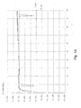
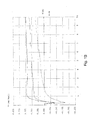
- the appearance of the silver layer can be seen in Fig. 2B.
- the layer is not evenly dense. It has a "cloudy" appearance.
Landscapes
- Chemical & Material Sciences (AREA)
- Engineering & Computer Science (AREA)
- Mechanical Engineering (AREA)
- Organic Chemistry (AREA)
- Chemical Kinetics & Catalysis (AREA)
- Materials Engineering (AREA)
- Metallurgy (AREA)
- Manufacturing & Machinery (AREA)
- General Chemical & Material Sciences (AREA)
- Microelectronics & Electronic Packaging (AREA)
- Chemically Coating (AREA)
- Electroplating Methods And Accessories (AREA)
- Manufacturing Of Printed Wiring (AREA)
- Laminated Bodies (AREA)
- Electrodes Of Semiconductors (AREA)
- Preventing Corrosion Or Incrustation Of Metals (AREA)
- Organic Low-Molecular-Weight Compounds And Preparation Thereof (AREA)
- Electroplating And Plating Baths Therefor (AREA)
Priority Applications (15)
| Application Number | Priority Date | Filing Date | Title |
|---|---|---|---|
| EP02090262A EP1245697A3 (fr) | 2002-07-17 | 2002-07-17 | Procédé de dépôt d'argent sans courant |
| PCT/EP2002/009997 WO2004007798A1 (fr) | 2002-07-17 | 2002-09-06 | Depot d'argent par immersion |
| AU2002368066A AU2002368066A1 (en) | 2002-07-17 | 2002-09-06 | Immersion plating of silver |
| KR1020057000834A KR20050029220A (ko) | 2002-07-17 | 2002-09-06 | 은의 침지도금 |
| US10/521,085 US7479305B2 (en) | 2002-07-17 | 2002-09-06 | Immersion plating of silver |
| AT02807595T ATE364739T1 (de) | 2002-07-17 | 2002-09-06 | Verfahren zum aussenstromlosen abscheiden von silber |
| BR0215769-1A BR0215769A (pt) | 2002-07-17 | 2002-09-06 | Chapeamento por imersão de prata |
| DE60220723T DE60220723T2 (de) | 2002-07-17 | 2002-09-06 | Verfahren zum aussenstromlosen abscheiden von silber |
| CNB028293274A CN100564594C (zh) | 2002-07-17 | 2002-09-06 | 银的浸镀 |
| ES02807595T ES2287363T3 (es) | 2002-07-17 | 2002-09-06 | Revestimiento de plata, por inmersion. |
| EP02807595A EP1521862B1 (fr) | 2002-07-17 | 2002-09-06 | Depot d'argent par immersion |
| JP2004520358A JP4194556B2 (ja) | 2002-07-17 | 2002-09-06 | 銀の浸漬めっき |
| CA002484757A CA2484757A1 (fr) | 2002-07-17 | 2002-09-06 | Depot d'argent par immersion |
| MYPI20023480A MY140935A (en) | 2002-07-17 | 2002-09-19 | Immersion plating of silver |
| TW91121598A TWI291998B (en) | 2002-07-17 | 2002-09-20 | Immersion plating of silver |
Applications Claiming Priority (1)
| Application Number | Priority Date | Filing Date | Title |
|---|---|---|---|
| EP02090262A EP1245697A3 (fr) | 2002-07-17 | 2002-07-17 | Procédé de dépôt d'argent sans courant |
Publications (2)
| Publication Number | Publication Date |
|---|---|
| EP1245697A2 true EP1245697A2 (fr) | 2002-10-02 |
| EP1245697A3 EP1245697A3 (fr) | 2003-02-19 |
Family
ID=8185607
Family Applications (2)
| Application Number | Title | Priority Date | Filing Date |
|---|---|---|---|
| EP02090262A Withdrawn EP1245697A3 (fr) | 2002-07-17 | 2002-07-17 | Procédé de dépôt d'argent sans courant |
| EP02807595A Expired - Lifetime EP1521862B1 (fr) | 2002-07-17 | 2002-09-06 | Depot d'argent par immersion |
Family Applications After (1)
| Application Number | Title | Priority Date | Filing Date |
|---|---|---|---|
| EP02807595A Expired - Lifetime EP1521862B1 (fr) | 2002-07-17 | 2002-09-06 | Depot d'argent par immersion |
Country Status (13)
| Country | Link |
|---|---|
| US (1) | US7479305B2 (fr) |
| EP (2) | EP1245697A3 (fr) |
| JP (1) | JP4194556B2 (fr) |
| KR (1) | KR20050029220A (fr) |
| CN (1) | CN100564594C (fr) |
| AT (1) | ATE364739T1 (fr) |
| AU (1) | AU2002368066A1 (fr) |
| BR (1) | BR0215769A (fr) |
| CA (1) | CA2484757A1 (fr) |
| DE (1) | DE60220723T2 (fr) |
| ES (1) | ES2287363T3 (fr) |
| MY (1) | MY140935A (fr) |
| WO (1) | WO2004007798A1 (fr) |
Cited By (2)
| Publication number | Priority date | Publication date | Assignee | Title |
|---|---|---|---|---|
| WO2003104527A1 (fr) * | 2002-06-11 | 2003-12-18 | Atotech Deutschland Gmbh | Solution acide pour le depot d'argent et procede de depot d'une couche d'argent sur des surfaces metalliques |
| CN113638019A (zh) * | 2021-08-13 | 2021-11-12 | 安徽师范大学 | 一种电镀厚银的铜基工件及其制作方法 |
Families Citing this family (12)
| Publication number | Priority date | Publication date | Assignee | Title |
|---|---|---|---|---|
| US8349393B2 (en) | 2004-07-29 | 2013-01-08 | Enthone Inc. | Silver plating in electronics manufacture |
| WO2006095851A1 (fr) * | 2005-03-11 | 2006-09-14 | Hitachi Chemical Co., Ltd. | Procede de traitement d’une surface de cuivre et cuivre |
| WO2007033188A2 (fr) * | 2005-09-12 | 2007-03-22 | University Of Dayton | Depot autocatalytique active par substrat (seed) de nanoparticules metalliques sur des nanotubes de carbone |
| EP2213766A4 (fr) * | 2007-10-22 | 2014-01-22 | Nat Inst For Materials Science | Procédé de dépôt autocatalytique pour film de revêtement d'alliage et liquide de dépôt |
| EP2453041B1 (fr) * | 2010-11-10 | 2014-02-12 | Atotech Deutschland GmbH | Solution et procédé pour le prétraitement de surfaces de cuivre à l'aide d'un composé N-alcoxylé qui favorise l'adhésion |
| EP2528089B1 (fr) * | 2011-05-23 | 2014-03-05 | Alchimer | Procédé pour la formation d'une connexion électrique verticale dans une structure semi-conductrice stratifiée |
| EP2581470B1 (fr) * | 2011-10-12 | 2016-09-28 | ATOTECH Deutschland GmbH | Composition de bain de placage au palladium anélectrolytique |
| EP2784180B1 (fr) * | 2013-03-25 | 2015-12-30 | ATOTECH Deutschland GmbH | Procédé d'activation d'une surface de cuivre pour dépôt anélectrolytique |
| EP3251825A1 (fr) | 2016-05-31 | 2017-12-06 | Boegli-Gravures S.A. | Procédé et dispositif de gaufrage de matériau plan |
| CN108315725A (zh) * | 2018-01-11 | 2018-07-24 | 广东禾木科技有限公司 | 一种银键合丝表面的杂质的去除方法 |
| JP7285123B2 (ja) * | 2019-04-10 | 2023-06-01 | 上村工業株式会社 | 金めっき方法及びめっき皮膜 |
| CN111778498B (zh) * | 2020-07-02 | 2024-04-26 | 深圳市化讯半导体材料有限公司 | 一种镀膜结构及其制备方法 |
Family Cites Families (18)
| Publication number | Priority date | Publication date | Assignee | Title |
|---|---|---|---|---|
| GB967681A (en) * | 1959-12-31 | 1964-08-26 | Mond Nickel Co Ltd | Improvements relating to the formation of metallic coatings |
| US3917885A (en) * | 1974-04-26 | 1975-11-04 | Engelhard Min & Chem | Electroless gold plating process |
| US4529667A (en) * | 1983-04-06 | 1985-07-16 | The Furukawa Electric Company, Ltd. | Silver-coated electric composite materials |
| JPS60241291A (ja) * | 1984-05-16 | 1985-11-30 | 株式会社東芝 | 印刷配線板の製造方法 |
| US5882802A (en) * | 1988-08-29 | 1999-03-16 | Ostolski; Marian J. | Noble metal coated, seeded bimetallic non-noble metal powders |
| JP2754828B2 (ja) | 1990-02-08 | 1998-05-20 | 松下電器産業株式会社 | プリント配線板の製造方法 |
| JPH06299375A (ja) | 1993-02-18 | 1994-10-25 | Murata:Kk | はんだ、無電解はんだ、銀、ニッケル、亜鉛、銅、銅合金等 の金属の表面処理方法 |
| GB9425031D0 (en) * | 1994-12-09 | 1995-02-08 | Alpha Metals Ltd | Printed circuit board manufacture |
| JP3594724B2 (ja) | 1995-09-29 | 2004-12-02 | 大日本印刷株式会社 | リードフレームの部分貴金属めっき方法 |
| KR100266726B1 (ko) * | 1995-09-29 | 2000-09-15 | 기타지마 요시토시 | 리드프레임과 이 리드프레임을 갖춘 반도체장치 |
| US5733599A (en) * | 1996-03-22 | 1998-03-31 | Macdermid, Incorporated | Method for enhancing the solderability of a surface |
| JP3532046B2 (ja) | 1996-10-25 | 2004-05-31 | 株式会社大和化成研究所 | 非シアン置換銀めっき浴 |
| JP2000505151A (ja) | 1996-11-21 | 2000-04-25 | コーニンクレッカ フィリップス エレクトロニクス エヌ ヴィ | ガラス基板に銀層を設ける方法 |
| JPH10330950A (ja) | 1997-06-02 | 1998-12-15 | Nippon Parkerizing Co Ltd | 改良充填置換析出型めっき金属材料及びその製造方法 |
| JP2000212763A (ja) | 1999-01-19 | 2000-08-02 | Shipley Far East Ltd | 銀合金メッキ浴及びそれを用いる銀合金被膜の形成方法 |
| DE10050862C2 (de) | 2000-10-06 | 2002-08-01 | Atotech Deutschland Gmbh | Bad und Verfahren zum stromlosen Abscheiden von Silber auf Metalloberflächen |
| JP2002180259A (ja) | 2000-12-12 | 2002-06-26 | Shipley Co Llc | めっき液における金属析出促進化合物および該化合物を含むめっき液 |
| US20030000846A1 (en) * | 2001-05-25 | 2003-01-02 | Shipley Company, L.L.C. | Plating method |
-
2002
- 2002-07-17 EP EP02090262A patent/EP1245697A3/fr not_active Withdrawn
- 2002-09-06 CN CNB028293274A patent/CN100564594C/zh not_active Expired - Fee Related
- 2002-09-06 ES ES02807595T patent/ES2287363T3/es not_active Expired - Lifetime
- 2002-09-06 DE DE60220723T patent/DE60220723T2/de not_active Expired - Lifetime
- 2002-09-06 JP JP2004520358A patent/JP4194556B2/ja not_active Expired - Fee Related
- 2002-09-06 US US10/521,085 patent/US7479305B2/en not_active Expired - Fee Related
- 2002-09-06 AU AU2002368066A patent/AU2002368066A1/en not_active Abandoned
- 2002-09-06 CA CA002484757A patent/CA2484757A1/fr not_active Abandoned
- 2002-09-06 BR BR0215769-1A patent/BR0215769A/pt not_active IP Right Cessation
- 2002-09-06 WO PCT/EP2002/009997 patent/WO2004007798A1/fr not_active Ceased
- 2002-09-06 EP EP02807595A patent/EP1521862B1/fr not_active Expired - Lifetime
- 2002-09-06 KR KR1020057000834A patent/KR20050029220A/ko not_active Ceased
- 2002-09-06 AT AT02807595T patent/ATE364739T1/de active
- 2002-09-19 MY MYPI20023480A patent/MY140935A/en unknown
Cited By (2)
| Publication number | Priority date | Publication date | Assignee | Title |
|---|---|---|---|---|
| WO2003104527A1 (fr) * | 2002-06-11 | 2003-12-18 | Atotech Deutschland Gmbh | Solution acide pour le depot d'argent et procede de depot d'une couche d'argent sur des surfaces metalliques |
| CN113638019A (zh) * | 2021-08-13 | 2021-11-12 | 安徽师范大学 | 一种电镀厚银的铜基工件及其制作方法 |
Also Published As
| Publication number | Publication date |
|---|---|
| JP4194556B2 (ja) | 2008-12-10 |
| AU2002368066A1 (en) | 2004-02-02 |
| EP1245697A3 (fr) | 2003-02-19 |
| DE60220723D1 (de) | 2007-07-26 |
| ES2287363T3 (es) | 2007-12-16 |
| JP2005538246A (ja) | 2005-12-15 |
| CN100564594C (zh) | 2009-12-02 |
| US20060165909A1 (en) | 2006-07-27 |
| WO2004007798A1 (fr) | 2004-01-22 |
| KR20050029220A (ko) | 2005-03-24 |
| ATE364739T1 (de) | 2007-07-15 |
| DE60220723T2 (de) | 2008-03-06 |
| US7479305B2 (en) | 2009-01-20 |
| EP1521862A1 (fr) | 2005-04-13 |
| BR0215769A (pt) | 2005-03-15 |
| CA2484757A1 (fr) | 2004-01-22 |
| CN1639385A (zh) | 2005-07-13 |
| MY140935A (en) | 2010-02-12 |
| EP1521862B1 (fr) | 2007-06-13 |
Similar Documents
| Publication | Publication Date | Title |
|---|---|---|
| DE60105305T2 (de) | Bad und verfahren zur stromlosen plattierung von silber auf metallischen oberflächen | |
| DE69511434T2 (de) | Herstellung von gedruckten schaltungen | |
| DE69728812T2 (de) | Verfahren zur Erhöhung der Lötbarkeit einer Oberfläche | |
| DE69509116T2 (de) | Beschichtung mit silber | |
| DE10165046B4 (de) | Verfahren zum Herstellen einer Schaltungsplatte unter Anwendung einer Zusammensetzung zum Mikroätzen | |
| DE102009037855B4 (de) | Verfahren zur Oberflächenbehandlung von Aluminium oder Aluminiumlegierungen | |
| DE69218892T2 (de) | Komplexierungsmittel für das Zinnplattieren nach der Austauschmethode | |
| DE69518166T2 (de) | Beschichten von kupfer | |
| DE10313517B4 (de) | Lösung zum Ätzen von Kupfer, Verfahren zum Vorbehandeln einer Schicht aus Kupfer sowie Anwendung des Verfahrens | |
| DE60220723T2 (de) | Verfahren zum aussenstromlosen abscheiden von silber | |
| DE3750282T2 (de) | Verfahren zur Metallplattierung. | |
| EP1615484A1 (fr) | Article avec une couche d'un polymère électroconducteur et procédé de sa production | |
| DE69215014T2 (de) | Bad und Verfahren zur stromlosen Beschichtung mit Zinn oder Zinn-Blei-Legierung | |
| DE3242899A1 (de) | Chemische entmetallisierungszusammensetzung zur entfernung von zinn und zinn-blei-legierungen vin einem metallisierten substrat und ein verfahren zur entfernung von loten aus zinn oder zinn-blei-legierungen von einem metallisierten substrat mit dieser zusammensetzung | |
| DE19740431C1 (de) | Verfahren zum Metallisieren eines elektrisch nichtleitende Oberflächenbereiche aufweisenden Substrats | |
| DE69217183T2 (de) | Verfahren zur Verlängerung der Benutzbarkeit eines Metallisierungsbades nach der Austauschmethode | |
| DE69635203T2 (de) | Beschichtungen und Verfahren, insbesondere für Leiterplatten | |
| KR101616731B1 (ko) | 금속 표면 처리 수용액 및 금속 표면상의 휘스커 억제방법 | |
| DE10226328B3 (de) | Saure Lösung zur Silberabscheidung und Verfahren zum Abscheiden von Silberschichten auf Metalloberflächen | |
| EP1082471A1 (fr) | Procede pour recouvrir des surfaces de cuivre ou d'alliage de cuivre avec une couche d'etain ou d'alliage d'etain | |
| WO2001076334A1 (fr) | Procede pour realiser des surfaces aptes au brasage et fonctionnelles sur des support de circuits | |
| DE102010011269B4 (de) | Verfahren zum Abscheiden einer für das Drahtbonden geeigneten Palladiumschicht auf Leiterbahnen einer Schaltungsträgerplatte und Verwendung eines Palladiumbades in dem Verfahren | |
| DE202005010364U1 (de) | Zinnbeschichtete flexible Leiterplatten mit geringer Neigung zur Whiskerbildung | |
| DE102005041533B3 (de) | Lösung und Verfahren zum Entfernen von ionischen Verunreinigungen von einem Werkstück | |
| DE69012454T2 (de) | Verfahren mit abgekürztem Zyklus zur Herstellung von gedruckten Leiterplatten und Zusammensetzung für die Anwendung. |
Legal Events
| Date | Code | Title | Description |
|---|---|---|---|
| PUAI | Public reference made under article 153(3) epc to a published international application that has entered the european phase |
Free format text: ORIGINAL CODE: 0009012 |
|
| AK | Designated contracting states |
Kind code of ref document: A2 Designated state(s): AT BE BG CH CY CZ DE DK EE ES FI FR GB GR IE IT LI LU MC NL PT SE SK TR |
|
| AX | Request for extension of the european patent |
Free format text: AL;LT;LV;MK;RO;SI |
|
| PUAL | Search report despatched |
Free format text: ORIGINAL CODE: 0009013 |
|
| RIC1 | Information provided on ipc code assigned before grant |
Ipc: 7C 23C 18/42 A |
|
| AK | Designated contracting states |
Designated state(s): AT BE BG CH CY CZ DE DK EE ES FI FR GB GR IE IT LI LU MC NL PT SE SK TR |
|
| AX | Request for extension of the european patent |
Extension state: AL LT LV MK RO SI |
|
| RTI1 | Title (correction) |
Free format text: PROCESS FOR ELECTROLESS SILVER PLATING |
|
| 17P | Request for examination filed |
Effective date: 20030122 |
|
| AKX | Designation fees paid |
Designated state(s): AT BE BG CH CY CZ DE DK EE ES FI FR GB GR IE IT LI LU MC NL PT SE SK TR |
|
| STAA | Information on the status of an ep patent application or granted ep patent |
Free format text: STATUS: THE APPLICATION HAS BEEN WITHDRAWN |
|
| 18W | Application withdrawn |
Effective date: 20041119 |
|
| REG | Reference to a national code |
Ref country code: HK Ref legal event code: WD Ref document number: 1047458 Country of ref document: HK |