EP1254517B2 - Frequenzteilung/vervielfachung mit minimierung des jitters - Google Patents
Frequenzteilung/vervielfachung mit minimierung des jitters Download PDFInfo
- Publication number
- EP1254517B2 EP1254517B2 EP00984376A EP00984376A EP1254517B2 EP 1254517 B2 EP1254517 B2 EP 1254517B2 EP 00984376 A EP00984376 A EP 00984376A EP 00984376 A EP00984376 A EP 00984376A EP 1254517 B2 EP1254517 B2 EP 1254517B2
- Authority
- EP
- European Patent Office
- Prior art keywords
- mux
- pll
- phase
- frequency
- output
- Prior art date
- Legal status (The legal status is an assumption and is not a legal conclusion. Google has not performed a legal analysis and makes no representation as to the accuracy of the status listed.)
- Expired - Lifetime
Links
- 238000000034 method Methods 0.000 abstract description 8
- 238000010586 diagram Methods 0.000 description 20
- 238000004891 communication Methods 0.000 description 4
- 230000010363 phase shift Effects 0.000 description 3
- 238000007493 shaping process Methods 0.000 description 3
- 238000001228 spectrum Methods 0.000 description 3
- 238000013459 approach Methods 0.000 description 2
- 230000008901 benefit Effects 0.000 description 2
- 238000013139 quantization Methods 0.000 description 2
- 230000002411 adverse Effects 0.000 description 1
- 230000002457 bidirectional effect Effects 0.000 description 1
- 230000007423 decrease Effects 0.000 description 1
- 230000003247 decreasing effect Effects 0.000 description 1
- 239000000835 fiber Substances 0.000 description 1
- 230000007274 generation of a signal involved in cell-cell signaling Effects 0.000 description 1
- 230000006872 improvement Effects 0.000 description 1
- 230000000737 periodic effect Effects 0.000 description 1
- 229920000729 poly(L-lysine) polymer Polymers 0.000 description 1
- 238000011084 recovery Methods 0.000 description 1
- 230000009467 reduction Effects 0.000 description 1
- 230000007704 transition Effects 0.000 description 1
Images


Classifications
-
- H—ELECTRICITY
- H03—ELECTRONIC CIRCUITRY
- H03L—AUTOMATIC CONTROL, STARTING, SYNCHRONISATION OR STABILISATION OF GENERATORS OF ELECTRONIC OSCILLATIONS OR PULSES
- H03L7/00—Automatic control of frequency or phase; Synchronisation
- H03L7/06—Automatic control of frequency or phase; Synchronisation using a reference signal applied to a frequency- or phase-locked loop
- H03L7/08—Details of the phase-locked loop
- H03L7/081—Details of the phase-locked loop provided with an additional controlled phase shifter
-
- H—ELECTRICITY
- H03—ELECTRONIC CIRCUITRY
- H03K—PULSE TECHNIQUE
- H03K23/00—Pulse counters comprising counting chains; Frequency dividers comprising counting chains
- H03K23/64—Pulse counters comprising counting chains; Frequency dividers comprising counting chains with a base or radix other than a power of two
- H03K23/68—Pulse counters comprising counting chains; Frequency dividers comprising counting chains with a base or radix other than a power of two with a base which is a non-integer
-
- H—ELECTRICITY
- H03—ELECTRONIC CIRCUITRY
- H03L—AUTOMATIC CONTROL, STARTING, SYNCHRONISATION OR STABILISATION OF GENERATORS OF ELECTRONIC OSCILLATIONS OR PULSES
- H03L7/00—Automatic control of frequency or phase; Synchronisation
- H03L7/06—Automatic control of frequency or phase; Synchronisation using a reference signal applied to a frequency- or phase-locked loop
- H03L7/08—Details of the phase-locked loop
- H03L7/099—Details of the phase-locked loop concerning mainly the controlled oscillator of the loop
- H03L7/0995—Details of the phase-locked loop concerning mainly the controlled oscillator of the loop the oscillator comprising a ring oscillator
- H03L7/0996—Selecting a signal among the plurality of phase-shifted signals produced by the ring oscillator
-
- H—ELECTRICITY
- H03—ELECTRONIC CIRCUITRY
- H03L—AUTOMATIC CONTROL, STARTING, SYNCHRONISATION OR STABILISATION OF GENERATORS OF ELECTRONIC OSCILLATIONS OR PULSES
- H03L7/00—Automatic control of frequency or phase; Synchronisation
- H03L7/06—Automatic control of frequency or phase; Synchronisation using a reference signal applied to a frequency- or phase-locked loop
- H03L7/16—Indirect frequency synthesis, i.e. generating a desired one of a number of predetermined frequencies using a frequency- or phase-locked loop
- H03L7/18—Indirect frequency synthesis, i.e. generating a desired one of a number of predetermined frequencies using a frequency- or phase-locked loop using a frequency divider or counter in the loop
Definitions
- the present invention is directed to a system for dividing or multiplying a reference frequency signal by a non-integer number while minimizing the introduction of timing jitter to the resultant output frequency signal.
- Such systems may range anywhere from broadcast or cablecast HDTV systems, local area and wide area network (LAN, WAN) systems, fiber to the home (FTTH) applications and board-to-board interconnections in exchange systems and computers.
- LAN local area and wide area network
- FTTH fiber to the home
- bidirectional data communication is in digital form and, accordingly, clock and data recovery circuitry is a key component of the efficient functioning of modern data communications systems.
- the ability to regenerate binary data is an inherent advantage of transmitting information digitally as opposed to transmitting such information in analog form.
- the transmitted binary data must be regenerated with the fewest possible number of bit errors, requiring low noise and timing jitter (phase noise) at the clock generation source.
- low jitters are important for ensuring low error rates.
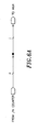
- Clock signal generation is traditionally performed by a Phase-Lock-Loop (PLL) system such as that illustrated in FIG. 1 .
- PLL Phase-Lock-Loop
- a PLL operates to compare the frequency and/or phase of an incoming serial datastream to a periodic reference clock signal generated by an oscillator circuit, and to adjust the operational frequency and phase characteristics of the oscillator until its output stream is "locked” in both frequency and phase to the data signal.
- Frequency division and/or frequency multiplication can be used to generate multiple clock phases from a PLL.
- FIG. 1 shows a typical PLL circuit that is used to perform a frequency signal multiplication (or division) function.
- a reference signal (“IN") is applied to one input of the Phase/Frequency Detector 10 where the phase and frequency of a feedback clock from a divider circuit 19 is compared.
- the Phase/Frequency detector 10 circuit outputs signals 16 & 18 to the charge pump circuit 12 indicating whether the feedback clock from the divider circuit is lower or higher in frequency and ahead or behind in phase.
- the charge pump converts the signals from the Phase/Frequency detector typically into analog current signals that are filtered by the Filter 13.
- the filtered signal is then output to the Voltage Controlled Oscillator (VCO) 14 which produces an output signal which is typically the output of the PLL ("OUT").
- VCO Voltage Controlled Oscillator
- the output signal of the VCO is input to the divider circuit 19, which divides the frequency of the output signal by an integer "N" in this example.
- the output signal of the divider circuit is input to the phase detector circuit completing the PLL. In this case, the output signal of the PLL is limited to integer multiples of the reference signal.
- Non-integer multiply/divide functions can also be implemented by designing the divider circuit 19 of FIG. 1A to appropriately suppress predetermined clock cycles to its input signal at a specific rate defined by a number "K", thereby decreasing its effective divide ratio by K+1/K.
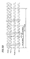
- FIG. 1B is an exemplary timing diagram for a conventional non-integer division.
- FOUT FVCO x K/(K+1), that is dividing FVCO by K+1/K.
- prior art-type PLL circuits do not provide an integrated, low-cost, and simple frequency division/multiplication with low jitter. Accordingly, for high-speed PLLs, there is a demonstrated need for a frequency division/multiplication with low jitter which is designed and constructed such that jitters are substantially minimized.
- US-A-5 889 436 relates to the preamble of claim 1.
- GB-A-2 325 803 relates to a method and an apparatus for digital frequency generation by cyclically selecting the outputs from a multi-phase oscillator.
- WO 90 060 17 relates to a circuit comprising a phase locked loop configured as a frequency multiplier capable of non-integral feedback path division.
- the present invention enables full flexibility to produce frequency multiplication/division by any non-integer output signal frequency (for example, (K+1)/K, or K/(K-1)) relative to a reference signal frequency, while simultaneously maintaining low jitter performance.
- any non-integer output signal frequency for example, (K+1)/K, or K/(K-1)
- the present invention minimizes jitters caused by frequency multiplication/division by a number of jitter reduction schemes and different combinations of those schemes.
- a frequency multiplication by a non-integer number such as K/(K-1) can be achieved by increasing the number of the available clock phases to M and then shifting the output clock in an opposite way by one, every K/M cycle.
- This technique of frequency division/multiplication decreases the jitter from T to T/M, resulting in a jitter improvement by a factor of M, because the discarded cycle is now 1/M of the original cycle.
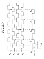
- Exemplary timing diagrams for this technique of frequency division/multiplication are illustrated in FIG. 3A and 3B , respectively.
- the shifting function may be performed by a MUX or any other signal shifter.
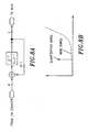
- FIG. 2 shows an exemplary implementation of this scheme.
- VCO 20 is capable of producing M phases of clocks.
- MUX 21 is added to the output of the VCO to implement the phase shifting every K/M cycles.
- Counter 23 controls the select signals for MUX 21 and the feedback clock is divided by N in block 22. Note that, for simplicity reasons, the charge pump 12 of FIG. 1A is included in PD 10 of FIG. 2 .
- FIG. 3A is a simplified timing diagram for the circuit of FIG. 2 for performing frequency division.
- the MUX switches from phase PH0 to phase PH1 and thus the first pulse of OUT signal is extended to the next phase, i.e., phase PH1, producing a phase shift of T/M.
- the MUX next switches from phase PH1 to phase PH2. This repeats every K/M cycles.
- FIG. 3C shows a noise spectrum diagram for the resulting jitter.
- the frequency of noise is related to how often the phase is shifted, that is the value of M.
- the energy of the noise is related to the jitter.
- the MUX next switches from phase PH1 to phase PH2. This repeats every K/4 cycles.
- the MUX goes through all the phases from phase PH0 to phase PH3 and back to phase PH0 resulting in K cycles in (K+1)T seconds. This increases the period from T to T+T/4 and divides the frequency by (K+1)/K. Consequently, the jitter is reduced to T/4.
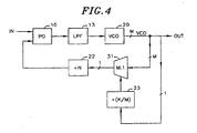
- MUX 21 of FIG. 2 may be placed in the feedback loop of the PLL, i.e. , between VCO 20 and PD 10, as shown by MUX 31 in FIG. 4 .
- the input of the MUX 31 is driven by a divide-by-K/M circuit 23 to select one out of M inputs of the MUX.
- this scheme feeds back the output of the phase shift to PD 10 through the low pass filter 13 and thus smoothes the clock transition when the phase is shifted from phase PH(k) to phase PH(k ⁇ 1), resulting in low jitter generation at the output of the VCO.
- the jitter energy is further reduced by the low pass filter of the PLL.
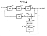
- the above scheme may be enhanced by using various quantizers as illustrated in FIG. 5 .
- the output of the divide-by-Q 43 is quantized by quantizer 44 to drive MUX 31 selector.
- a truncator may be used as a quantizer, as shown in FIG. 6A .
- FIG. 6B is a simplified circuit diagram of the modified PLL using the truncator of FIG. 6A .
- the quantizer is used in combination with the modified PLL of FIG. 2 , where the MUX is not in the feedback loop of the PLL.
- FIG. 7A shows another example of a quantizer used in one embodiment of the present invention.
- a random number generator generates a random number to be added to the value of the counter, resulting in shifting the phase in random.
- the random number is added to the value of the counter at a specific time.
- at random time intervals one is added to or subtracted from the value of the counter. The addition and subtraction of one at random time intervals should average out as zero.
- FIG. 7C is a simplified circuit diagram of the modified PLL using the random number generator of FIG. 7A .
- the random number generator is used in combination with the modified PLL of FIG. 2 , where the MUX is at the output of the VCO.
- FIG. 8C is a simplified circuit diagram of the modified PLL using the integrator of FIG. 8A .
- the noise shaping block is used in combination with the modified PLL of FIG. 2 , where the MUX is at the output of the VCO.
Landscapes
- Stabilization Of Oscillater, Synchronisation, Frequency Synthesizers (AREA)
- Manipulation Of Pulses (AREA)
- Dc Digital Transmission (AREA)
Claims (1)
- Ein integrierter Schaltkreis für Frequenzmultiplikation / Frequenzteilung mit niedrigem Jitter zur Multiplikation / Teilung einer Frequenz eines Referenzsignals, wobei der Schaltkreis aufweist:ein Phase Lock Loop, PLL, zur Generierung einer Anzahl M von Taktphasen aus dem Referenzsignal; undein Signalshifter, welcher als Multiplexer, MUX (31), ausgestaltet ist und welcher elektrisch mit dem PLL gekoppelt ist, um das Referenzsignal jeden K/M Zyklus um ein Phase zu verschieben, wobei der MUX (31) elektrisch an den Ausgang des PLL gekoppelt ist und wobei (K+1)/K eine Teilerzahl und K/(K-1) eine Multiplikatorzahl ist,dadurch gekennzeichnet, dass
der Schaltkreis weiter aufweist:- einen Quantizer (44), der elektrisch mit dem MUX (31) gekoppelt ist, um den Eingang des MUX zu treiben;- eine Teile-durch-Q-Schaltung (43), welche eine der M Taktphasen empfängt und mit ihrem Ausgang an den Quantizer (44) gekoppelt ist; und- eine Teilerschaltung (22), welche an den Ausgang des MUX (31) gekoppelt ist, wobei sich beide in einer Rückführungsschleife des PLL befinden,in welcher die Teilerschaltung (22) die Frequenz des Ausgangssignals des MUX (31) durch eine ganze Zahl teilt.
Applications Claiming Priority (3)
| Application Number | Priority Date | Filing Date | Title |
|---|---|---|---|
| US17062199P | 1999-12-14 | 1999-12-14 | |
| US170621P | 1999-12-14 | ||
| PCT/US2000/033908 WO2001045263A1 (en) | 1999-12-14 | 2000-12-14 | Frequency division/multiplication with jitter minimization |
Publications (3)
| Publication Number | Publication Date |
|---|---|
| EP1254517A1 EP1254517A1 (de) | 2002-11-06 |
| EP1254517B1 EP1254517B1 (de) | 2005-06-08 |
| EP1254517B2 true EP1254517B2 (de) | 2009-02-11 |
Family
ID=22620640
Family Applications (1)
| Application Number | Title | Priority Date | Filing Date |
|---|---|---|---|
| EP00984376A Expired - Lifetime EP1254517B2 (de) | 1999-12-14 | 2000-12-14 | Frequenzteilung/vervielfachung mit minimierung des jitters |
Country Status (6)
| Country | Link |
|---|---|
| US (4) | US6441655B1 (de) |
| EP (1) | EP1254517B2 (de) |
| AT (1) | ATE297607T1 (de) |
| AU (1) | AU2100301A (de) |
| DE (1) | DE60020742T3 (de) |
| WO (1) | WO2001045263A1 (de) |
Families Citing this family (39)
| Publication number | Priority date | Publication date | Assignee | Title |
|---|---|---|---|---|
| US6515526B2 (en) * | 1999-04-26 | 2003-02-04 | Ando Electric Co., Ltd. | Phase fluctuation generation |
| US6748408B1 (en) * | 1999-10-21 | 2004-06-08 | International Buisness Machines Corporation | Programmable non-integer fractional divider |
| EP1254517B2 (de) * | 1999-12-14 | 2009-02-11 | Broadcom Corporation | Frequenzteilung/vervielfachung mit minimierung des jitters |
| US6807552B2 (en) * | 2000-12-20 | 2004-10-19 | International Business Machines Corporation | Programmable non-integer fractional divider |
| US7242229B1 (en) | 2001-05-06 | 2007-07-10 | Altera Corporation | Phase locked loop (PLL) and delay locked loop (DLL) counter and delay element programming in user mode |
| US6992792B2 (en) * | 2001-06-29 | 2006-01-31 | Electronics For Imaging, Inc. | Digital pulse width modulator for use in electrostatic printing mechanisms |
| US7035367B2 (en) * | 2001-09-26 | 2006-04-25 | Nokia Corporation | Fractional multi-modulus prescaler |
| US6542013B1 (en) * | 2002-01-02 | 2003-04-01 | Intel Corporation | Fractional divisors for multiple-phase PLL systems |
| FR2841405B1 (fr) | 2002-06-19 | 2004-08-06 | Commissariat Energie Atomique | Boucle a verrouillage de retard |
| US20040125869A1 (en) * | 2002-12-31 | 2004-07-01 | May Michael R. | Method and apparatus for non-intrusive transceiver property adjustment |
| US7003274B1 (en) * | 2003-03-05 | 2006-02-21 | Cisco Systems Wireless Networking (Australia) Pty Limited | Frequency synthesizer and synthesis method for generating a multiband local oscillator signal |
| US7295077B2 (en) * | 2003-05-02 | 2007-11-13 | Silicon Laboratories Inc. | Multi-frequency clock synthesizer |
| US7288998B2 (en) * | 2003-05-02 | 2007-10-30 | Silicon Laboratories Inc. | Voltage controlled clock synthesizer |
| US7187241B2 (en) * | 2003-05-02 | 2007-03-06 | Silicon Laboratories Inc. | Calibration of oscillator devices |
| US7064617B2 (en) * | 2003-05-02 | 2006-06-20 | Silicon Laboratories Inc. | Method and apparatus for temperature compensation |
| US7436227B2 (en) * | 2003-05-02 | 2008-10-14 | Silicon Laboratories Inc. | Dual loop architecture useful for a programmable clock source and clock multiplier applications |
| US6956793B2 (en) * | 2003-11-20 | 2005-10-18 | International Business Machines Corporation | Phase clock selector for generating a non-integer frequency division |
| CA2453292A1 (en) * | 2004-01-07 | 2005-07-07 | John W. Bogdan | Noise filtering edge detectors |
| US7113009B2 (en) * | 2004-03-24 | 2006-09-26 | Silicon Laboratories Inc. | Programmable frequency divider |
| US7405601B2 (en) * | 2004-05-03 | 2008-07-29 | Silicon Laboratories Inc. | High-speed divider with pulse-width control |
| US7187216B2 (en) * | 2004-05-03 | 2007-03-06 | Silicon Laboratories Inc. | Phase selectable divider circuit |
| US7042260B2 (en) * | 2004-06-14 | 2006-05-09 | Micron Technology, Inc. | Low power and low timing jitter phase-lock loop and method |
| EP1624575B1 (de) * | 2004-08-06 | 2009-01-28 | Stmicroelectronics SA | Frequenzsynthetiser Architektur |
| US20060132200A1 (en) * | 2004-12-22 | 2006-06-22 | Markus Dietl | Fractional-N divider, fractional-N phase locked loop and method of dividing a frequency f of an output signal by N, wherein N is a non-integer |
| US20060215296A1 (en) * | 2005-03-24 | 2006-09-28 | Gennum Corporation | Bidirectional referenceless communication circuit |
| US7873133B2 (en) * | 2005-06-30 | 2011-01-18 | Infinera Corporation | Recovery of client clock without jitter |
| US7417565B2 (en) * | 2005-09-13 | 2008-08-26 | Research In Motion Limited | Keyboard for hand-held devices |
| JP4745127B2 (ja) * | 2006-05-23 | 2011-08-10 | ルネサスエレクトロニクス株式会社 | クロック切替回路 |
| US7551009B2 (en) * | 2007-02-28 | 2009-06-23 | Silicon Laboratories Inc. | High-speed divider with reduced power consumption |
| US7605665B2 (en) * | 2007-05-25 | 2009-10-20 | Broadcom Corporation | Fractional-N phase locked loop |
| EP2238416A1 (de) * | 2008-02-01 | 2010-10-13 | Stichting Voor De Technische Wetenschappen | Synchrone phasenerkennungsschaltung |
| US8086974B2 (en) * | 2008-03-31 | 2011-12-27 | International Business Machines Corporation | Structure for fractional-N phased-lock-loop (PLL) system |
| US7705641B2 (en) * | 2008-04-23 | 2010-04-27 | Ralink Technology Corporation | Fast response phase-locked loop charge-pump driven by low voltage input |
| US7944257B2 (en) * | 2009-05-14 | 2011-05-17 | Ralink Technology (Singapore) Corporation | Method and system of optimizing a control system using low voltage and high-speed switching |
| EP2288031A1 (de) | 2009-07-28 | 2011-02-23 | Nxp B.V. | Frequenzteiler |
| US9110875B2 (en) * | 2010-02-11 | 2015-08-18 | International Business Machines Corporation | XML post-processing hardware acceleration |
| US8710879B2 (en) * | 2012-07-06 | 2014-04-29 | Silicon Integrated System Corp. | Apparatus and method for multiplying frequency of a clock signal |
| JP7367616B2 (ja) * | 2020-06-08 | 2023-10-24 | 株式会社デンソー | 噴射制御装置 |
| CN114726367B (zh) * | 2022-06-02 | 2022-08-23 | 上海泰矽微电子有限公司 | 一种基于门控的低抖动时钟分频电路及控制方法 |
Citations (2)
| Publication number | Priority date | Publication date | Assignee | Title |
|---|---|---|---|---|
| CA2233831A1 (en) † | 1998-03-31 | 1999-09-30 | Tom Riley | Digital-sigma fractional-n synthesizer |
| US5986512A (en) † | 1997-12-12 | 1999-11-16 | Telefonaktiebolaget L M Ericsson (Publ) | Σ-Δ modulator-controlled phase-locked-loop circuit |
Family Cites Families (11)
| Publication number | Priority date | Publication date | Assignee | Title |
|---|---|---|---|---|
| WO1990006017A1 (en) * | 1988-11-07 | 1990-05-31 | Level One Communications, Inc. | Frequency multiplier with non-integer feedback divider |
| CA2001266C (en) * | 1989-10-23 | 1996-08-06 | John Robert Long | Digital phase aligner and method for its operation |
| CA2191967C (en) * | 1994-06-17 | 2000-03-21 | Josef Schneider | High-pressure cleaning appliance with safety insulation |
| US6616996B1 (en) * | 1994-10-28 | 2003-09-09 | Medsource Trenton, Inc. | Variable stiffness microtubing and method of manufacture |
| US6044123A (en) * | 1996-10-17 | 2000-03-28 | Hitachi Micro Systems, Inc. | Method and apparatus for fast clock recovery phase-locked loop with training capability |
| US5889436A (en) * | 1996-11-01 | 1999-03-30 | National Semiconductor Corporation | Phase locked loop fractional pulse swallowing frequency synthesizer |
| GB2325803B (en) * | 1997-05-30 | 1999-09-29 | Lsi Logic Corp | Digital frequency generation method and apparatus |
| US6157694A (en) * | 1998-12-09 | 2000-12-05 | Lucent Technologies, Inc. | Fractional frequency divider |
| US6661863B1 (en) * | 1999-04-16 | 2003-12-09 | Infineon Technologies North America Corp. | Phase mixer |
| US6181213B1 (en) * | 1999-06-14 | 2001-01-30 | Realtek Semiconductor Corp. | Phase-locked loop having a multi-phase voltage controlled oscillator |
| EP1254517B2 (de) | 1999-12-14 | 2009-02-11 | Broadcom Corporation | Frequenzteilung/vervielfachung mit minimierung des jitters |
-
2000
- 2000-12-14 EP EP00984376A patent/EP1254517B2/de not_active Expired - Lifetime
- 2000-12-14 AT AT00984376T patent/ATE297607T1/de not_active IP Right Cessation
- 2000-12-14 DE DE60020742T patent/DE60020742T3/de not_active Expired - Lifetime
- 2000-12-14 AU AU21003/01A patent/AU2100301A/en not_active Abandoned
- 2000-12-14 WO PCT/US2000/033908 patent/WO2001045263A1/en not_active Ceased
- 2000-12-14 US US09/736,612 patent/US6441655B1/en not_active Expired - Lifetime
-
2002
- 2002-08-26 US US10/227,259 patent/US6714056B2/en not_active Expired - Lifetime
-
2004
- 2004-02-23 US US10/782,890 patent/US6930519B2/en not_active Expired - Lifetime
-
2005
- 2005-02-23 US US11/062,495 patent/US7005899B2/en not_active Expired - Lifetime
Patent Citations (2)
| Publication number | Priority date | Publication date | Assignee | Title |
|---|---|---|---|---|
| US5986512A (en) † | 1997-12-12 | 1999-11-16 | Telefonaktiebolaget L M Ericsson (Publ) | Σ-Δ modulator-controlled phase-locked-loop circuit |
| CA2233831A1 (en) † | 1998-03-31 | 1999-09-30 | Tom Riley | Digital-sigma fractional-n synthesizer |
Also Published As
| Publication number | Publication date |
|---|---|
| EP1254517A1 (de) | 2002-11-06 |
| US20040169534A1 (en) | 2004-09-02 |
| DE60020742T3 (de) | 2009-09-17 |
| US20030058009A1 (en) | 2003-03-27 |
| WO2001045263A1 (en) | 2001-06-21 |
| DE60020742D1 (de) | 2005-07-14 |
| US20050140411A1 (en) | 2005-06-30 |
| US6441655B1 (en) | 2002-08-27 |
| EP1254517B1 (de) | 2005-06-08 |
| US6714056B2 (en) | 2004-03-30 |
| AU2100301A (en) | 2001-06-25 |
| ATE297607T1 (de) | 2005-06-15 |
| DE60020742T2 (de) | 2006-03-16 |
| US6930519B2 (en) | 2005-08-16 |
| US20020027459A1 (en) | 2002-03-07 |
| US7005899B2 (en) | 2006-02-28 |
Similar Documents
| Publication | Publication Date | Title |
|---|---|---|
| EP1254517B2 (de) | Frequenzteilung/vervielfachung mit minimierung des jitters | |
| CN1127200C (zh) | 用数字字调整的频率合成电路 | |
| EP1148648B1 (de) | Frequenzsynthetisierer | |
| US7969251B2 (en) | Fractional divider | |
| CN100555874C (zh) | 分数n频率合成器内的数字增量求和调制器 | |
| US8278982B2 (en) | Low noise fractional divider using a multiphase oscillator | |
| US7605665B2 (en) | Fractional-N phase locked loop | |
| US6642800B2 (en) | Spurious-free fractional-N frequency synthesizer with multi-phase network circuit | |
| US6937685B2 (en) | Apparatus and method for counting high-speed early/late pulses from a high speed phase detector using a pulse accumulator | |
| US20070291173A1 (en) | Phase lock loop and digital control oscillator thereof | |
| WO2007130750A2 (en) | Phase-slipping phase-locked loop | |
| US20100283525A1 (en) | Phase control device and data communication system using it | |
| US7212050B2 (en) | System and method for synthesizing a clock at digital wrapper (FEC) and base frequencies using one precision resonator | |
| EP4175180B1 (de) | Schaltung und verfahren zur fraktionierten teilung von hochfrequenztaktsignalen | |
| CN1973438A (zh) | 频率合成器和方法 | |
| WO1998016013A1 (en) | Frequency synthesizer having phase error feedback for waveform selection | |
| US8867696B2 (en) | Fractional frequency divider | |
| JP2003179490A (ja) | フラクショナルn周波数シンセサイザ | |
| CN120165684B (zh) | 展频小数分频控制电路、小数分频锁相环和芯片 | |
| WO2002027938A2 (en) | High resolution, low jitter frequency synthesizer | |
| HK1025685B (en) | Frequency synthesis circuit tuned by digital words |
Legal Events
| Date | Code | Title | Description |
|---|---|---|---|
| PUAI | Public reference made under article 153(3) epc to a published international application that has entered the european phase |
Free format text: ORIGINAL CODE: 0009012 |
|
| 17P | Request for examination filed |
Effective date: 20020715 |
|
| AK | Designated contracting states |
Kind code of ref document: A1 Designated state(s): AT BE CH CY DE DK ES FI FR GB GR IE IT LI LU MC NL PT SE TR |
|
| AX | Request for extension of the european patent |
Free format text: AL;LT;LV;MK;RO;SI |
|
| 17Q | First examination report despatched |
Effective date: 20030728 |
|
| GRAP | Despatch of communication of intention to grant a patent |
Free format text: ORIGINAL CODE: EPIDOSNIGR1 |
|
| GRAS | Grant fee paid |
Free format text: ORIGINAL CODE: EPIDOSNIGR3 |
|
| GRAA | (expected) grant |
Free format text: ORIGINAL CODE: 0009210 |
|
| AK | Designated contracting states |
Kind code of ref document: B1 Designated state(s): AT BE CH CY DE DK ES FI FR GB GR IE IT LI LU MC NL PT SE TR |
|
| PG25 | Lapsed in a contracting state [announced via postgrant information from national office to epo] |
Ref country code: NL Free format text: LAPSE BECAUSE OF FAILURE TO SUBMIT A TRANSLATION OF THE DESCRIPTION OR TO PAY THE FEE WITHIN THE PRESCRIBED TIME-LIMIT Effective date: 20050608 Ref country code: AT Free format text: LAPSE BECAUSE OF FAILURE TO SUBMIT A TRANSLATION OF THE DESCRIPTION OR TO PAY THE FEE WITHIN THE PRESCRIBED TIME-LIMIT Effective date: 20050608 Ref country code: LI Free format text: LAPSE BECAUSE OF FAILURE TO SUBMIT A TRANSLATION OF THE DESCRIPTION OR TO PAY THE FEE WITHIN THE PRESCRIBED TIME-LIMIT Effective date: 20050608 Ref country code: TR Free format text: LAPSE BECAUSE OF FAILURE TO SUBMIT A TRANSLATION OF THE DESCRIPTION OR TO PAY THE FEE WITHIN THE PRESCRIBED TIME-LIMIT Effective date: 20050608 Ref country code: CH Free format text: LAPSE BECAUSE OF FAILURE TO SUBMIT A TRANSLATION OF THE DESCRIPTION OR TO PAY THE FEE WITHIN THE PRESCRIBED TIME-LIMIT Effective date: 20050608 Ref country code: BE Free format text: LAPSE BECAUSE OF FAILURE TO SUBMIT A TRANSLATION OF THE DESCRIPTION OR TO PAY THE FEE WITHIN THE PRESCRIBED TIME-LIMIT Effective date: 20050608 Ref country code: FI Free format text: LAPSE BECAUSE OF FAILURE TO SUBMIT A TRANSLATION OF THE DESCRIPTION OR TO PAY THE FEE WITHIN THE PRESCRIBED TIME-LIMIT Effective date: 20050608 Ref country code: IT Free format text: LAPSE BECAUSE OF FAILURE TO SUBMIT A TRANSLATION OF THE DESCRIPTION OR TO PAY THE FEE WITHIN THE PRESCRIBED TIME-LIMIT;WARNING: LAPSES OF ITALIAN PATENTS WITH EFFECTIVE DATE BEFORE 2007 MAY HAVE OCCURRED AT ANY TIME BEFORE 2007. THE CORRECT EFFECTIVE DATE MAY BE DIFFERENT FROM THE ONE RECORDED. Effective date: 20050608 |
|
| REG | Reference to a national code |
Ref country code: GB Ref legal event code: FG4D |
|
| REG | Reference to a national code |
Ref country code: CH Ref legal event code: EP |
|
| REF | Corresponds to: |
Ref document number: 60020742 Country of ref document: DE Date of ref document: 20050714 Kind code of ref document: P |
|
| REG | Reference to a national code |
Ref country code: IE Ref legal event code: FG4D |
|
| PG25 | Lapsed in a contracting state [announced via postgrant information from national office to epo] |
Ref country code: SE Free format text: LAPSE BECAUSE OF FAILURE TO SUBMIT A TRANSLATION OF THE DESCRIPTION OR TO PAY THE FEE WITHIN THE PRESCRIBED TIME-LIMIT Effective date: 20050908 Ref country code: DK Free format text: LAPSE BECAUSE OF FAILURE TO SUBMIT A TRANSLATION OF THE DESCRIPTION OR TO PAY THE FEE WITHIN THE PRESCRIBED TIME-LIMIT Effective date: 20050908 Ref country code: GR Free format text: LAPSE BECAUSE OF FAILURE TO SUBMIT A TRANSLATION OF THE DESCRIPTION OR TO PAY THE FEE WITHIN THE PRESCRIBED TIME-LIMIT Effective date: 20050908 |
|
| PG25 | Lapsed in a contracting state [announced via postgrant information from national office to epo] |
Ref country code: ES Free format text: LAPSE BECAUSE OF FAILURE TO SUBMIT A TRANSLATION OF THE DESCRIPTION OR TO PAY THE FEE WITHIN THE PRESCRIBED TIME-LIMIT Effective date: 20050919 |
|
| PG25 | Lapsed in a contracting state [announced via postgrant information from national office to epo] |
Ref country code: PT Free format text: LAPSE BECAUSE OF FAILURE TO SUBMIT A TRANSLATION OF THE DESCRIPTION OR TO PAY THE FEE WITHIN THE PRESCRIBED TIME-LIMIT Effective date: 20051114 |
|
| NLV1 | Nl: lapsed or annulled due to failure to fulfill the requirements of art. 29p and 29m of the patents act | ||
| PG25 | Lapsed in a contracting state [announced via postgrant information from national office to epo] |
Ref country code: IE Free format text: LAPSE BECAUSE OF NON-PAYMENT OF DUE FEES Effective date: 20051214 Ref country code: CY Free format text: LAPSE BECAUSE OF FAILURE TO SUBMIT A TRANSLATION OF THE DESCRIPTION OR TO PAY THE FEE WITHIN THE PRESCRIBED TIME-LIMIT Effective date: 20051214 |
|
| REG | Reference to a national code |
Ref country code: CH Ref legal event code: PL |
|
| PG25 | Lapsed in a contracting state [announced via postgrant information from national office to epo] |
Ref country code: MC Free format text: LAPSE BECAUSE OF NON-PAYMENT OF DUE FEES Effective date: 20051231 Ref country code: LU Free format text: LAPSE BECAUSE OF NON-PAYMENT OF DUE FEES Effective date: 20051231 |
|
| PLBI | Opposition filed |
Free format text: ORIGINAL CODE: 0009260 |
|
| ET | Fr: translation filed | ||
| PLAX | Notice of opposition and request to file observation + time limit sent |
Free format text: ORIGINAL CODE: EPIDOSNOBS2 |
|
| 26 | Opposition filed |
Opponent name: QUALCOMM INCORPORATED Effective date: 20060308 |
|
| PLAF | Information modified related to communication of a notice of opposition and request to file observations + time limit |
Free format text: ORIGINAL CODE: EPIDOSCOBS2 |
|
| REG | Reference to a national code |
Ref country code: IE Ref legal event code: MM4A |
|
| PLBB | Reply of patent proprietor to notice(s) of opposition received |
Free format text: ORIGINAL CODE: EPIDOSNOBS3 |
|
| RAP2 | Party data changed (patent owner data changed or rights of a patent transferred) |
Owner name: BROADCOM CORPORATION |
|
| REG | Reference to a national code |
Ref country code: FR Ref legal event code: CA |
|
| PLAY | Examination report in opposition despatched + time limit |
Free format text: ORIGINAL CODE: EPIDOSNORE2 |
|
| PLBC | Reply to examination report in opposition received |
Free format text: ORIGINAL CODE: EPIDOSNORE3 |
|
| PLAB | Opposition data, opponent's data or that of the opponent's representative modified |
Free format text: ORIGINAL CODE: 0009299OPPO |
|
| PUAH | Patent maintained in amended form |
Free format text: ORIGINAL CODE: 0009272 |
|
| STAA | Information on the status of an ep patent application or granted ep patent |
Free format text: STATUS: PATENT MAINTAINED AS AMENDED |
|
| 27A | Patent maintained in amended form |
Effective date: 20090211 |
|
| AK | Designated contracting states |
Kind code of ref document: B2 Designated state(s): AT BE CH CY DE DK ES FI FR GB GR IE IT LI LU MC NL PT SE TR |
|
| REG | Reference to a national code |
Ref country code: ES Ref legal event code: FD2A Effective date: 20051215 |
|
| REG | Reference to a national code |
Ref country code: FR Ref legal event code: PLFP Year of fee payment: 16 |
|
| PGFP | Annual fee paid to national office [announced via postgrant information from national office to epo] |
Ref country code: GB Payment date: 20151221 Year of fee payment: 16 |
|
| PGFP | Annual fee paid to national office [announced via postgrant information from national office to epo] |
Ref country code: FR Payment date: 20151218 Year of fee payment: 16 |
|
| REG | Reference to a national code |
Ref country code: DE Ref legal event code: R082 Ref document number: 60020742 Country of ref document: DE Representative=s name: BOSCH JEHLE PATENTANWALTSGESELLSCHAFT MBH, DE Ref country code: DE Ref legal event code: R081 Ref document number: 60020742 Country of ref document: DE Owner name: AVAGO TECHNOLOGIES INTERNATIONAL SALES PTE. LT, SG Free format text: FORMER OWNER: BROADCOM CORP., IRVINE, CALIF., US Ref country code: DE Ref legal event code: R081 Ref document number: 60020742 Country of ref document: DE Owner name: AVAGO TECHNOLOGIES GENERAL IP (SINGAPORE) PTE., SG Free format text: FORMER OWNER: BROADCOM CORP., IRVINE, CALIF., US |
|
| GBPC | Gb: european patent ceased through non-payment of renewal fee |
Effective date: 20161214 |
|
| REG | Reference to a national code |
Ref country code: FR Ref legal event code: ST Effective date: 20170831 |
|
| PG25 | Lapsed in a contracting state [announced via postgrant information from national office to epo] |
Ref country code: FR Free format text: LAPSE BECAUSE OF NON-PAYMENT OF DUE FEES Effective date: 20170102 |
|
| PG25 | Lapsed in a contracting state [announced via postgrant information from national office to epo] |
Ref country code: GB Free format text: LAPSE BECAUSE OF NON-PAYMENT OF DUE FEES Effective date: 20161214 |
|
| REG | Reference to a national code |
Ref country code: DE Ref legal event code: R082 Ref document number: 60020742 Country of ref document: DE Representative=s name: BOSCH JEHLE PATENTANWALTSGESELLSCHAFT MBH, DE Ref country code: DE Ref legal event code: R081 Ref document number: 60020742 Country of ref document: DE Owner name: AVAGO TECHNOLOGIES INTERNATIONAL SALES PTE. LT, SG Free format text: FORMER OWNER: AVAGO TECHNOLOGIES GENERAL IP (SINGAPORE) PTE. LTD., SINGAPORE, SG |
|
| PGFP | Annual fee paid to national office [announced via postgrant information from national office to epo] |
Ref country code: DE Payment date: 20191231 Year of fee payment: 20 |
|
| REG | Reference to a national code |
Ref country code: DE Ref legal event code: R071 Ref document number: 60020742 Country of ref document: DE |