EP1259060A2 - Dispositif d'imagerie pour générer un nombre de points d'image dans une ligne de projection - Google Patents
Dispositif d'imagerie pour générer un nombre de points d'image dans une ligne de projection Download PDFInfo
- Publication number
- EP1259060A2 EP1259060A2 EP02009280A EP02009280A EP1259060A2 EP 1259060 A2 EP1259060 A2 EP 1259060A2 EP 02009280 A EP02009280 A EP 02009280A EP 02009280 A EP02009280 A EP 02009280A EP 1259060 A2 EP1259060 A2 EP 1259060A2
- Authority
- EP
- European Patent Office
- Prior art keywords
- line
- light source
- projection
- light sources
- printing
- Prior art date
- Legal status (The legal status is an assumption and is not a legal conclusion. Google has not performed a legal analysis and makes no representation as to the accuracy of the status listed.)
- Granted
Links
Images



Classifications
-
- B—PERFORMING OPERATIONS; TRANSPORTING
- B41—PRINTING; LINING MACHINES; TYPEWRITERS; STAMPS
- B41J—TYPEWRITERS; SELECTIVE PRINTING MECHANISMS, i.e. MECHANISMS PRINTING OTHERWISE THAN FROM A FORME; CORRECTION OF TYPOGRAPHICAL ERRORS
- B41J2/00—Typewriters or selective printing mechanisms characterised by the printing or marking process for which they are designed
- B41J2/435—Typewriters or selective printing mechanisms characterised by the printing or marking process for which they are designed characterised by selective application of radiation to a printing material or impression-transfer material
- B41J2/447—Typewriters or selective printing mechanisms characterised by the printing or marking process for which they are designed characterised by selective application of radiation to a printing material or impression-transfer material using arrays of radiation sources
- B41J2/45—Typewriters or selective printing mechanisms characterised by the printing or marking process for which they are designed characterised by selective application of radiation to a printing material or impression-transfer material using arrays of radiation sources using light-emitting diode [LED] or laser arrays
-
- B—PERFORMING OPERATIONS; TRANSPORTING
- B41—PRINTING; LINING MACHINES; TYPEWRITERS; STAMPS
- B41C—PROCESSES FOR THE MANUFACTURE OR REPRODUCTION OF PRINTING SURFACES
- B41C1/00—Forme preparation
-
- B—PERFORMING OPERATIONS; TRANSPORTING
- B41—PRINTING; LINING MACHINES; TYPEWRITERS; STAMPS
- B41J—TYPEWRITERS; SELECTIVE PRINTING MECHANISMS, i.e. MECHANISMS PRINTING OTHERWISE THAN FROM A FORME; CORRECTION OF TYPOGRAPHICAL ERRORS
- B41J2/00—Typewriters or selective printing mechanisms characterised by the printing or marking process for which they are designed
- B41J2/435—Typewriters or selective printing mechanisms characterised by the printing or marking process for which they are designed characterised by selective application of radiation to a printing material or impression-transfer material
- B41J2/47—Typewriters or selective printing mechanisms characterised by the printing or marking process for which they are designed characterised by selective application of radiation to a printing material or impression-transfer material using the combination of scanning and modulation of light
- B41J2/471—Typewriters or selective printing mechanisms characterised by the printing or marking process for which they are designed characterised by selective application of radiation to a printing material or impression-transfer material using the combination of scanning and modulation of light using dot sequential main scanning by means of a light deflector, e.g. a rotating polygonal mirror
- B41J2/473—Typewriters or selective printing mechanisms characterised by the printing or marking process for which they are designed characterised by selective application of radiation to a printing material or impression-transfer material using the combination of scanning and modulation of light using dot sequential main scanning by means of a light deflector, e.g. a rotating polygonal mirror using multiple light beams, wavelengths or colours
-
- H—ELECTRICITY
- H04—ELECTRIC COMMUNICATION TECHNIQUE
- H04N—PICTORIAL COMMUNICATION, e.g. TELEVISION
- H04N1/00—Scanning, transmission or reproduction of documents or the like, e.g. facsimile transmission; Details thereof
- H04N1/04—Scanning arrangements, i.e. arrangements for the displacement of active reading or reproducing elements relative to the original or reproducing medium, or vice versa
- H04N1/047—Detection, control or error compensation of scanning velocity or position
- H04N1/053—Detection, control or error compensation of scanning velocity or position in main scanning direction, e.g. synchronisation of line start or picture elements in a line
-
- B—PERFORMING OPERATIONS; TRANSPORTING
- B41—PRINTING; LINING MACHINES; TYPEWRITERS; STAMPS
- B41C—PROCESSES FOR THE MANUFACTURE OR REPRODUCTION OF PRINTING SURFACES
- B41C1/00—Forme preparation
- B41C1/10—Forme preparation for lithographic printing; Master sheets for transferring a lithographic image to the forme
- B41C1/1075—Mechanical aspects of on-press plate preparation
-
- H—ELECTRICITY
- H04—ELECTRIC COMMUNICATION TECHNIQUE
- H04N—PICTORIAL COMMUNICATION, e.g. TELEVISION
- H04N1/00—Scanning, transmission or reproduction of documents or the like, e.g. facsimile transmission; Details thereof
- H04N1/04—Scanning arrangements, i.e. arrangements for the displacement of active reading or reproducing elements relative to the original or reproducing medium, or vice versa
- H04N1/06—Scanning arrangements, i.e. arrangements for the displacement of active reading or reproducing elements relative to the original or reproducing medium, or vice versa using cylindrical picture-bearing surfaces, i.e. scanning a main-scanning line substantially perpendicular to the axis and lying in a curved cylindrical surface
-
- H—ELECTRICITY
- H04—ELECTRIC COMMUNICATION TECHNIQUE
- H04N—PICTORIAL COMMUNICATION, e.g. TELEVISION
- H04N1/00—Scanning, transmission or reproduction of documents or the like, e.g. facsimile transmission; Details thereof
- H04N1/04—Scanning arrangements, i.e. arrangements for the displacement of active reading or reproducing elements relative to the original or reproducing medium, or vice versa
- H04N1/19—Scanning arrangements, i.e. arrangements for the displacement of active reading or reproducing elements relative to the original or reproducing medium, or vice versa using multi-element arrays
- H04N1/191—Scanning arrangements, i.e. arrangements for the displacement of active reading or reproducing elements relative to the original or reproducing medium, or vice versa using multi-element arrays the array comprising a one-dimensional [1D] array
- H04N1/1911—Simultaneously or substantially simultaneously scanning picture elements on more than one main scanning line, e.g. scanning in swaths
-
- H—ELECTRICITY
- H04—ELECTRIC COMMUNICATION TECHNIQUE
- H04N—PICTORIAL COMMUNICATION, e.g. TELEVISION
- H04N2201/00—Indexing scheme relating to scanning, transmission or reproduction of documents or the like, and to details thereof
- H04N2201/04—Scanning arrangements
- H04N2201/047—Detection, control or error compensation of scanning velocity or position
- H04N2201/04753—Control or error compensation of scanning position or velocity
- H04N2201/04758—Control or error compensation of scanning position or velocity by controlling the position of the scanned image area
- H04N2201/04767—Control or error compensation of scanning position or velocity by controlling the position of the scanned image area by controlling the timing of the signals, e.g. by controlling the frequency o phase of the pixel clock
- H04N2201/04781—Controlling the phase of the signals
- H04N2201/04786—Controlling a start time, e.g. for output of a line of data
Definitions
- the invention relates to an imaging device with a number of light sources, each having a distance s i , the index i counting the light sources, from an object line, for generating pixels of the light sources in a projection line of the object line on a printing form, which at least coincides with a speed component v perpendicular to the direction defined by the projection line and tangential to the surface of the printing form, and with a control device for switching each individual light source.
- Imaging optics for projecting the image are often optional Light sources emitted light on the printing form, often changing the Direction of propagation of the light or under beam shaping provided.
- the pixels of the light sources on the Printing form in a projection line typically when the printing form is on a So-called printing plate cylinder or plate cylinder is added, parallel to Cylinder axis. If the pixels are not on a projection line or in particular not parallel to the cylinder axis, image errors can occur on the printing form arise.
- the image points of the light sources lie with sufficient precision in an object plane, but are not arranged on an object line in this.
- the object line lies in the object plane.
- the object line can be a curve in the object plane with curved and straight sections; without restricting the generality, a straight object line is considered below.
- the individual light sources or emitters are each at a distance s i from an object line, i counting the individual emitters, at least two light sources being at a different distance from the object line. Typically, within the desired or required precision, this distance is not zero or cannot be neglected.
- an optical element In the direction of the slow axis, an optical element focuses the emitted Light on a spatial light modulator such that the light is any point Light source irradiates the entire active area of the spatial light modulator. It is a Another optical element is provided, which the light in the direction of the fast axis focused so that the desired spot size creates in the direction of the fast axis becomes.
- the optical system disclosed in document US 5,900,981 uses natural ones and / or artificially introduced aberrations to reduce the sensitivity to the smile effect, which occurs with most laser diode bars.
- a disadvantage of The optical system disclosed in this document is the high effort for the Adjustment of the arrangement of microlenses.
- US Pat. No. 6,044,096 describes a compact laser diode array with reduced asymmetry disclosed. It is intended to reduce the smile effect of the laser diode bar, by providing a plurality of thermal load elements for the majority of the individual Diode light sources are assigned.
- the thermal load elements are similar to that individual laser diode light sources with the exception that their output power is blocked. Every thermal load element is in direct contact with it assigned individual laser diodes, so that an efficient heat transfer can take place.
- the Operating temperature of the individual laser light source can be changed or set. Consequently, the position of two laser light sources relative to one another can be different Currents can be reached through the heat load elements assigned to them.
- a disadvantage of influencing the temperature of the smile effect is, for example, that the Wavelength of the radiation emitted by the laser light source is changed. Of Furthermore, fluctuations in the temperature control lead to shifts in the Position of the laser diode compared to the array axis.
- the light sources are switched on and after a switched off again after a certain time.
- the emitters are triggered by a trigger or trigger signal triggered at a certain trigger time.
- the pixel of a light source depending on Trigger time on the printing form is at a position with coordinates, which one Function of the trigger time.
- the Document US B 1 5,174,205 described device for the control of a Imaging device for a printing form, which during the Imaging process moved relative to the imaging device, exploited.
- the Image information is stored in a first memory, while correction data for the Control of the light sources are located in a second memory.
- the correction data are used to determine the time intervals between imaging shots of the light sources to change to deviations between the measured position of the printing form in the Compared to the imaging head and the actual position.
- US B1 5,163,368 discloses how a correction for each pixel can be made using its coordinates on the printing form. These coordinate values are stored in a table. With those in these documents Correction devices described can in particular change the size of the Printing form in their coordinate directions are taken into account and compensated.
- document DE 26 53 539 should also be mentioned, in which the delayed activation of an imaging device with a number of Light sources whose pixels meet a printing form at an angle, i.e. not parallel the coordinate lines of the geometry corresponding to the printing form Coordinate system.
- the one caused by the inclined position of the imaging device Offset compared to a coordinate axis with all being switched on at the same time Light sources are made by changing the recording data accordingly compensated.
- the original recording data assigned raster calculator to compensate for the offset even with several different delayed clock pulses, i.e. trigger signals or Control signals are applied.
- the object of the present invention is to provide an imaging device for a Print form to create which is a number of pixels on a projection line are arranged with a number of light sources, wherein at least two light sources a different distance from the object line exhibit.
- Imaging device with the features according to Claim 1 and by a method for generating pixels according to claim 9 solved.
- Advantageous embodiments and developments of the invention Imaging device and the inventive method are in the Characterized sub-claims.
- the imaging device comprises a number of light sources for generating pixels of the light sources in a projection line on a printing form.
- the light sources are each at a distance s i , the index i counting the light sources, from an object line in the object plane, which is defined by the light sources.
- the end mirrors of the laser resonators lie essentially in one plane on a substrate and can thus define an object plane.
- an object level can also be a level spatially behind an imaging optics arranged downstream of the light sources.
- the projection line comprises the points of the printing form on which the image of the object line comes to lie on the printing form at a first point in time.
- the projection line and the object line have a projection ratio k.
- a projection point of a light source is to be understood as the point on the printing form to which the light emitted by the light source would fall at a specific point in time if it was switched on at the said point in time.
- An image point of a light source is to be understood as the point on the printing form which the light emitted by the light source strikes at a specific point in time while the light source is actually switched on.
- the printing form moves at least with a speed component v perpendicular to the direction defined by the object line and tangential to Surface of the printing form, at least in the vicinity of the projection points of the light sources.
- the projection line defined as described above moves with the Printing form.
- the imaging device is a control device for switching everyone assigned to individual light sources. Switching includes switching everyone on individual light source, which then with a certain intensity in a certain Time interval emits light and the light source is switched off. Under trigger is in understood in this context that at least switching on is carried out. Intensity and exposure time for a pixel are a function of the imaging data. By means of the pixel passed over the printing form, a Pressure point generated.
- the device according to the invention is characterized in that the control device of the light sources is assigned a time delay device which shifts the triggering time of the control device for each light source depending on the respective distance s i of the light source from the object line.
- an advantageous subject line is a straight line Line in the object plane, in particular, is advantageous if the light sources in one Half-plane of the object line, which means by means of the object line straight line is limited.
- the invention is distinguished Imaging device characterized in that the control device a temporal Delay device is assigned, which is relative to the trigger time, that is Time of switching on, a first light source whose projection point on the Projection line of the object line comes to lie, so that by triggering the a pixel is generated on the projection line by the first light source, each other Light source of the number of light sources switches or triggers differently in time, that the corresponding or associated pixel on the projection line of the Item line is generated when the corresponding or associated one Projection point of the other light source lies on the projection line.
- the triggering time of the first light source at or after the first point in time the position of the projection line on the printing form is defined.
- a first light source in the invention Imaging device with a number of light sources is triggered when you Projection point comes to lie on the projection line of the object line, so that the corresponding or associated pixel lies on the projection line.
- the simultaneous triggering of any other light source in the imaging device would general cause that every pixel of every other light source is not on the Projection line lies because generally the projection points at the time of triggering the first light source do not lie on the projection line of the object line.
- every projection point of every other light source changes its position on the Printing form, also its position relative to that through the pixel of the first light source printing point set on the printing form or at the first defined point in time Line of projection of the object line on the printing form. After a certain amount of time every projection point of every other light source passes the projection line so that the Triggering this light source for imaging by a pixel on the Line of projection of the object line leads.
- Imaging device is considered to be delayed without limitation of generality Triggering described at the time of triggering a first light source.
- This representation is based on the idea that the first light source is the one whose Projection point due to the relative movement between the imaging device and Printing form is the first to reach the projection line of the object line. Is preferred chosen an object line for which it applies that all light sources in one half-plane of the object plane, which is through the plane passing through the object line Is just limited. It is clear to the person skilled in the art that if a Light source is called, its pixel on the projection line of the object line to lie only after pixels of several other light sources of the imaging device comes, for the several other light sources a premature release is required is.
- each trigger signal or Control signal to trigger imaging for each individual emitter via a Delay device or a delay circuit shifted in time so that the Deviation of the position of the individual light sources to an object line in the the light sources defined level is compensated.
- the light sources in the invention are preferred Imaging device around lasers, typically an array of diode lasers, in particular a one-dimensional array of diode lasers, for example arranged on a diode laser bar.
- diode laser bars is a major cause for an uneven position of the emitters to an object line, the so-called smile effect, as described in more detail above.
- the smile effect can be compensated in a simple way.
- the imaging device according to the invention can have imaging optics include.
- This imaging optics are preferably objects with a projection ratio map k. It can also be provided that beam-shaping elements, Light deflecting elements or light guiding elements, such as mirrors, optical fibers or the like, or elements for polarization rotation of the light are provided.
- the imaging optics typically comprise elements for divergence or Astigmatism correction of the light sources and / or elements for aberration correction.
- the printing form can be clamped on a cylinder or be included.
- the line of projection of the object line preferably runs essentially parallel to the cylinder axis about which the printing form is rotated can.
- the imaging device in the Can can be moved essentially parallel to the cylinder axis.
- the printing form moves uniformly with a speed component v perpendicular to the direction defined by the object line and tangential to the surface of the printing form.
- the speed component v is essentially constant.
- the imaging device can be used to generate a field of printing dots by rows of pixels, in particular for a field in which adjacent printing dots to be generated are spaced apart by a distance h. If the distance s i of a light source is greater than n times the distance h / k of adjacent pressure points, where n is a natural number and k is the projection ratio, the control of the light source in question can be carried out with the image information of the generating pressure point which is the smallest distance from Has projection line of the object line take place.
- the control device then switches the light source in such a way that in the delay time interval, points on the printing form have essentially covered the distance (ks i -nh), where k is the projection ratio between the object line and the projection line and n is Int (s i k / h), that is the largest natural multiple of h, for which nh is less than s i k.
- the method according to the invention for generating pixels from a number of light sources, each having a distance s i , the index i counting the light sources, from an object line in the plane defined by the light sources, in a projection line of the object line on a printing form, which at least with a speed component v perpendicular to the direction defined by the object line and tangential to the printing form surface, comprises the following steps.
- the exposure is triggered by a first light source when its projection point comes to lie on the projection line of the object line.
- a second light source is triggered with a time delay in order to trigger the first light source in such a way that the corresponding image point of the second light source also lies on the projection line of the object line, that is to say when the corresponding projection point of the second light source passes the projection line.
- An analogous procedure is provided for each additional light source in the imaging device with a number of light sources.
- One method for generating pixels from a number of light sources is one easy compensation of the smile effect of diode laser arrays possible without one To accept a reduction in the beam quality.
- the Delay device in the form of programmable logic is also great for one Number of emitters, for example greater than 20 individual light sources, a structure in a very compact design possible.
- the number of emitters or is advantageous Light sources have a prime or a prime power and the spacing of the Emitter projection points is a multiple of h, where the multiple is one is prime to the stated prime number or prime power.
- a printing press according to the invention with a feeder, at least one printing unit and one delivery includes at least one printing unit, which has an imaging device according to the invention.
- FIG. 1 shows the position of a number of light sources to an object line.
- FIG. 1 shows an example and without restricting the Generality seven light sources 12 and a subject line 14. For each light source 12 at the distance s the perpendicular from the center 18 of the light source 12 to the Item line 14 understood. In most cases, the item line 14 is in the Essentially parallel to a boundary line of the emitter surface of the light source 12 run, in Figure 1, however, is the general case in which also the distances s of the individual light sources are of different sizes.
- FIG 2 shows schematically a preferred embodiment of the invention Imaging device with a time delay device for deviating Circuit of individual light sources.
- the imaging module 10 consists of a individually controllable array of a number of light sources 12 typically Laser light sources, especially diode laser arrays.
- the light sources are generally located 12 not on an object line 14, but each have an individual Distance to this object line 14.
- the general example is shown in FIG Case shown that not all light sources 12 in a half-plane of the subject line lie, which is limited by the straight line running through the object line.
- the Light beams 24 emitted by the light sources 12 are generated by means of imaging optics 26 mapped onto pixels 210 on a printing form 28.
- the Pixels 210 to a projection line 16 which is the image of the object line 14 corresponds to an individual by the imaging optics 26 at a first point in time Distance on.
- the distance of a certain pixel 210 from the projection line 16 becomes with exclusion of imaging errors of the imaging optics 26 proportional to the distance of the light source 12 generating the pixel 210 to the object line 14 with the Proportionality factor of the projection ratio k of the imaging optics 26.
- the light sources 12 in the imaging module 10 can be in continuous laser operation be used. To generate individual light packets, the laser emission is for one certain time interval suppressed or interrupted accordingly. Since the printing form 28 relative to a speed component v to the imaging device Moved at least tangentially to the surface of the printing form 28, the image points 210 lie of the light sources 12 when the light sources 12 are all triggered simultaneously different trigger times at different coordinate positions on the Surface of the printing form 28. The projection line 16 of the object line 14 also moves the printing form 28.
- the imaging optics 26 can be reflective, transmitting, refractive or have similar optical components. These are preferably micro-optical components, i.e. components that are individual Light source 12 affect light emitted while the light from the others Light sources 12 remains unaffected by this component. Especially in the event that the light sources 12 are lasers, in particular diode lasers, can be achieved by the imaging optics 26 both an enlarging and reducing as well as in the two directions Different imaging scales parallel and perpendicular to the active zone of the laser have, which is particularly advantageous for divergence and / or aberration correction is.
- the surface of the printing form 28 is in its physical and / or chemical Properties changed by the laser radiation, so that by exposure to a certain intensity and during a certain time interval image information for a pressure point is written.
- the imaging module 10 is located on a Cooling element 212, for example a copper heat sink with cooling water flow.
- the Imaging module 10 is by means of a line for power supply and control 214 connected to a control device 216.
- the control device 216 has individual components with which it is possible to use the individual light sources 12 of the Control or regulate arrays separately from each other.
- Using a line to Control of the cooling element 218 is the cooling element 212 with the temperature control 220 connected.
- a delay device 222 which in a compact design with the imaging module 10 is integrated.
- the delay device 222 is via the Connection 224 is linked to the control device 216, so this is assigned.
- the delay device 222 preferably comprises one programmable logic or an ASIC, an application-specific integrated Circuit.
- a Counter device with counter start values for each other light source 12 in Imaging module 10 started. It can be provided that in the Delay device 222 receives the imaging data for individual light sources 12 in are stored in a memory.
- the counting device counts 12 for each light source Start value back to zero. By reaching the zero value, the Corresponding light source 12 switched and the transfer of the corresponding data triggered at this emitter.
- FIG. 3 shows an embodiment of the imaging device according to the invention with a time delay device for imaging a printing form, which on a rotatable cylinder is accommodated.
- the imaging module 30 has examples three light sources, so that three light beams 32 are generated, which by means of the Imaging optics 34 are imaged on three pixels 310 on the printing form 38.
- the three pixels have an individual distance from a projection line 18. Without Limitation of generality, a projection line 18 is shown, for which applies that the three pixels 310 lie in a half-plane of the projection plane, which is indicated by the straight line is limited by the projection line 18.
- the printing form 38 is located on a cylinder 36 which is rotatable about its axis of symmetry 35. This Rotation is indicated by the arrow R.
- the imaging module 30 is essentially parallel to the Axis of symmetry 35 of the cylinder 36 can be moved in essentially linear ways can, which is marked with the double arrow T.
- For continuous Imaging rotates the cylinder 36 with the printing form 38 received on it according to the Rotational movement R, and the imaging module 30 translates along the cylinder 36 according to the direction of movement T.
- the way of Projection points or pixels 310 are indicated by lines 312.
- FIGS. 4, 5, 6 and 7 serve to explain using an example without restricting the generality, such as with the imaging device according to the invention with a number of light sources, each having a distance s i , the index i counting the light sources, to an object line in of the plane defined by the light sources, for generating pixels of the light sources in a projection line of the object line on a printing form, which moves at least with a speed component v perpendicular to that through the object line and tangential to the surface of the printing form, printing points by pixels on the projection line or a field of pressure points is generated by rows.
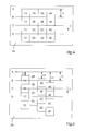
- FIG. 4 is an exemplary sketch to explain the notation used with regard to the position of printing dots to be imaged on a printing form 28.
- FIG. 4 is used without restriction of the generality of four emitters or Light sources, which exemplify a field of 4 x 4 pressure points Generate pixels of the light sources on the printing form. It is exemplified here assumed that a regular Cartesian field is to be described. However, there are other patterns of pressure points to be imaged are also conceivable.
- the extension of a Pressure point or the distance of adjacent pressure points to each other, measured by a center point to the next center point is denoted by h.
- Pressure points shown as squares are simplified Pressure points shown as squares; the actual shape is due to the shape of the Imaging light beam with its process parameters such as intensity, exposure time, Relative speed between printing form and imaging light beam and the like, certainly.
- the pressure points in the field are with a number-letter combination denotes: The number corresponds to the index, which the individual light sources, especially lasers, while the letter counts the order of the alphabet Imaging steps lying one after the other.
- Figure 4 shows a first Projection line A, a second projection line B, a third projection line C and one fourth projection line D, which is the projection points of the four not shown here Emitters or light sources happen one after the other when the printing form coincides with a speed component v in the direction of the arrow relative to the light sources comprehensive imaging module moves. If the projection point is a first Light source or a first emitter comes to lie on the first projection line A, becomes a trigger or switching signal to trigger the imaging by the pixel generated so that a pressure point is set.
- FIG. 5 is a schematic illustration of an exemplary position of pixels without compensation on the printing form 28 by the time delay device Imaging device according to the invention shown.
- An example happens here without Limitation of the generality of the projection point of the second light source as time first the first projection line A. If all light sources are controlled at the same time due to the individual distance between each light source Object line in the plane defined by the light sources the pixels of the other light sources compared to the start edge of the pixel 2A or added.
- the pixels generated by the first light source have one as an example first offset L1, the pixels generated by the third light source a third Offset L3 and the pixels generated by the fourth light source a fourth offset L4 on.
- FIG. 5 shows that the pixels of the fourth light source by more than a pressure point length h from the corresponding projection line lie.
- FIG. 6 is a schematic illustration of the exemplary position of pixels without compensation on the printing form 28 by changing the control of the light sources with those projection points or pixels whose distance is greater than that Pressure point distance is.
- FIG. 7 is a schematic representation of the position of pixels with compensation by delayed activation of the light sources after a triggering time of a first light source considered in time, here the second light source as an example.
- the data transfer and the triggering of the light sources can be delayed after a triggering time of a first light source.
- the trigger signal corresponding to the passage of the first projection line A through the projection point of the second light source defines delayed triggering times individually for each light source in such a way that the pixels of the light sources come to lie on the first projection line A in order to generate pressure points.
- the desired field of pressure points is generated for each additional projection line by means of iteration.
- the delay device should be operated with a signal frequency which is a multiple of the frequency of the original control signal.
- the shift is implemented by means of delayed activation by the delay device, which has, for example, programmable logic, an ASIC, discrete electronics or the like.
- the distances s i , the index i counts the light sources, and the projection ratio k between the object line and the projection line are made available to the delay electronics in a suitable form, for example by storage in a storage unit. From this information, the speed component v of the relative movement between printing form and imaging device with known speed profile of the printing form, for example a uniform movement, the delay device can determine start values for counters, which are each assigned to a light source.
- the distances s i can be determined in the context of an object line in the object plane as part of a calibration or measurement. It is clear in this context that the distances s i of the light sources to a first object line can be converted to distances to a second object line using simple arithmetic.
Landscapes
- Engineering & Computer Science (AREA)
- Health & Medical Sciences (AREA)
- Signal Processing (AREA)
- Manufacturing & Machinery (AREA)
- Physics & Mathematics (AREA)
- Optics & Photonics (AREA)
- Multimedia (AREA)
- General Health & Medical Sciences (AREA)
- Toxicology (AREA)
- Exposure And Positioning Against Photoresist Photosensitive Materials (AREA)
- Manufacture Or Reproduction Of Printing Formes (AREA)
- Printers Or Recording Devices Using Electromagnetic And Radiation Means (AREA)
- Editing Of Facsimile Originals (AREA)
- Studio Devices (AREA)
Applications Claiming Priority (2)
| Application Number | Priority Date | Filing Date | Title |
|---|---|---|---|
| DE10124215 | 2001-05-18 | ||
| DE10124215A DE10124215A1 (de) | 2001-05-18 | 2001-05-18 | Bebilderungseinrichtung zur Erzeugung einer Anzahl von Bildpunkten in einer Projektionslinie |
Publications (3)
| Publication Number | Publication Date |
|---|---|
| EP1259060A2 true EP1259060A2 (fr) | 2002-11-20 |
| EP1259060A3 EP1259060A3 (fr) | 2005-05-18 |
| EP1259060B1 EP1259060B1 (fr) | 2012-03-07 |
Family
ID=7685246
Family Applications (1)
| Application Number | Title | Priority Date | Filing Date |
|---|---|---|---|
| EP02009280A Expired - Lifetime EP1259060B1 (fr) | 2001-05-18 | 2002-04-29 | Dispositif d'imagerie pour générer un nombre de points d'image dans une ligne de projection |
Country Status (9)
| Country | Link |
|---|---|
| US (1) | US7843480B2 (fr) |
| EP (1) | EP1259060B1 (fr) |
| JP (1) | JP2003035958A (fr) |
| CN (1) | CN1268983C (fr) |
| AT (1) | ATE548196T1 (fr) |
| CA (1) | CA2380985A1 (fr) |
| CZ (1) | CZ20021103A3 (fr) |
| DE (1) | DE10124215A1 (fr) |
| IL (1) | IL149615A0 (fr) |
Families Citing this family (6)
| Publication number | Priority date | Publication date | Assignee | Title |
|---|---|---|---|---|
| JP4505250B2 (ja) | 2003-06-16 | 2010-07-21 | ハイデルベルガー ドルツクマシーネン アクチエンゲゼルシヤフト | 版のための描画装置および光学要素を描画装置に配置する方法 |
| JP5095946B2 (ja) * | 2005-02-18 | 2012-12-12 | ハイデルベルガー ドルツクマシーネン アクチエンゲゼルシヤフト | 少なくとも1つのレーザダイオードバーを備える版の画像付け装置 |
| DE202008004285U1 (de) | 2008-03-28 | 2008-07-03 | Man Roland Druckmaschinen Ag | Bebilderungseinrichtung |
| DE102013102599A1 (de) * | 2013-03-14 | 2014-09-18 | Limo Patentverwaltung Gmbh & Co. Kg | Beleuchtungsvorrichtung |
| JP7543982B2 (ja) * | 2021-05-27 | 2024-09-03 | 市光工業株式会社 | 車両用投影装置、その動作方法、及び車両用灯具 |
| CN119668036B (zh) * | 2023-09-19 | 2025-11-21 | 深圳市先地图像科技有限公司 | 一种激光直写图像检测方法、系统及相关设备 |
Citations (5)
| Publication number | Priority date | Publication date | Assignee | Title |
|---|---|---|---|---|
| DE2653539A1 (de) | 1976-11-25 | 1978-06-01 | Hell Rudolf Dr Ing Gmbh | Anordnung zur aufzeichnung von gerasterten halbtonbildern |
| US5163368A (en) | 1988-08-19 | 1992-11-17 | Presst, Inc. | Printing apparatus with image error correction and ink regulation control |
| US5174205A (en) | 1991-01-09 | 1992-12-29 | Kline John F | Controller for spark discharge imaging |
| US5900981A (en) | 1997-04-15 | 1999-05-04 | Scitex Corporation Ltd. | Optical system for illuminating a spatial light modulator |
| US6044096A (en) | 1997-11-03 | 2000-03-28 | Sdl, Inc. | Packaged laser diode array system and method with reduced asymmetry |
Family Cites Families (19)
| Publication number | Priority date | Publication date | Assignee | Title |
|---|---|---|---|---|
| JPS6031417B2 (ja) * | 1980-01-30 | 1985-07-22 | 沖電気工業株式会社 | 光走査装置 |
| DE3376727D1 (en) * | 1983-11-01 | 1988-06-23 | Agfa Gevaert Nv | Recording apparatus |
| DE9219213U1 (de) * | 1991-01-09 | 2000-08-03 | Presstek, Inc., Hudson, N.H. | Steuerungsgerät für Funkenentladungsbilderzeugung |
| US5274394A (en) * | 1991-05-22 | 1993-12-28 | Xerox Corporation | Electronic adjustment of slow scan image registration in an image recording apparatus |
| US5379698A (en) * | 1992-07-20 | 1995-01-10 | Presstek, Inc. | Lithographic printing members for use with laser-discharge imaging |
| DE9302494U1 (de) * | 1993-02-20 | 1993-04-22 | Man Roland Druckmaschinen Ag, 63069 Offenbach | Anordnung zum Bebildern einer Schicht auf der Oberfläche eines Formzylinders |
| JPH07333938A (ja) * | 1994-06-09 | 1995-12-22 | Canon Inc | カラ−画像形成装置 |
| DE19602307A1 (de) * | 1996-01-23 | 1997-07-24 | Roland Man Druckmasch | Druckmaschine |
| US5854651A (en) * | 1996-05-31 | 1998-12-29 | Eastman Kodak Company | Optically correcting deviations from straightness of laser emitter arrays |
| US6141030A (en) * | 1997-04-24 | 2000-10-31 | Konica Corporation | Laser exposure unit including plural laser beam sources differing in wavelength |
| US6091891A (en) * | 1997-05-09 | 2000-07-18 | Lexmark International, Inc. | Method and apparatus for calibrating delay lines to create gray levels in continuous tone printing |
| JP3381582B2 (ja) * | 1997-06-27 | 2003-03-04 | カシオ電子工業株式会社 | 光書き込みヘッド駆動装置、及びその装置を使用する光書き込みヘッド駆動方法 |
| JPH1110949A (ja) * | 1997-06-27 | 1999-01-19 | Ricoh Co Ltd | マルチビーム画像形成装置 |
| JPH11138898A (ja) * | 1997-11-11 | 1999-05-25 | Fuji Photo Film Co Ltd | 露光装置及び露光方法 |
| EP1020304B1 (fr) * | 1999-01-18 | 2006-04-05 | Fuji Photo Film Co., Ltd. | Procédé d'impression lithographique et imprimante l'utilisant |
| US6390579B1 (en) * | 1999-04-15 | 2002-05-21 | Hewlett-Packard Company | Pulse width modulator using delay-line technology with automatic calibration of delays to desired operating frequency |
| US6532029B1 (en) * | 2000-11-21 | 2003-03-11 | Aetas Technology Incorporated | Imaging-offset compensation methods and systems |
| US6603498B1 (en) * | 2000-11-28 | 2003-08-05 | Coherent, Inc. | Printer head with linear array of individually addressable diode-lasers |
| US6819351B2 (en) * | 2001-05-30 | 2004-11-16 | Nexpress Solutions Llc | Coarse and fine electronic bow correction for a writer |
-
2001
- 2001-05-18 DE DE10124215A patent/DE10124215A1/de not_active Ceased
-
2002
- 2002-03-28 CZ CZ20021103A patent/CZ20021103A3/cs unknown
- 2002-04-09 CA CA002380985A patent/CA2380985A1/fr not_active Abandoned
- 2002-04-29 AT AT02009280T patent/ATE548196T1/de active
- 2002-04-29 EP EP02009280A patent/EP1259060B1/fr not_active Expired - Lifetime
- 2002-05-13 IL IL14961502A patent/IL149615A0/xx not_active IP Right Cessation
- 2002-05-15 US US10/146,245 patent/US7843480B2/en not_active Expired - Fee Related
- 2002-05-17 JP JP2002142924A patent/JP2003035958A/ja active Pending
- 2002-05-17 CN CN02120274.5A patent/CN1268983C/zh not_active Expired - Fee Related
Patent Citations (7)
| Publication number | Priority date | Publication date | Assignee | Title |
|---|---|---|---|---|
| DE2653539A1 (de) | 1976-11-25 | 1978-06-01 | Hell Rudolf Dr Ing Gmbh | Anordnung zur aufzeichnung von gerasterten halbtonbildern |
| US5163368A (en) | 1988-08-19 | 1992-11-17 | Presst, Inc. | Printing apparatus with image error correction and ink regulation control |
| US5163368B1 (en) | 1988-08-19 | 1999-08-24 | Presstek Inc | Printing apparatus with image error correction and ink regulation control |
| US5174205A (en) | 1991-01-09 | 1992-12-29 | Kline John F | Controller for spark discharge imaging |
| US5174205B1 (en) | 1991-01-09 | 1999-10-05 | Presstek Inc | Controller for spark discharge imaging |
| US5900981A (en) | 1997-04-15 | 1999-05-04 | Scitex Corporation Ltd. | Optical system for illuminating a spatial light modulator |
| US6044096A (en) | 1997-11-03 | 2000-03-28 | Sdl, Inc. | Packaged laser diode array system and method with reduced asymmetry |
Also Published As
| Publication number | Publication date |
|---|---|
| US7843480B2 (en) | 2010-11-30 |
| CN1386635A (zh) | 2002-12-25 |
| HK1051837A1 (en) | 2003-08-22 |
| CN1268983C (zh) | 2006-08-09 |
| EP1259060A3 (fr) | 2005-05-18 |
| EP1259060B1 (fr) | 2012-03-07 |
| DE10124215A1 (de) | 2002-11-21 |
| CZ20021103A3 (cs) | 2003-01-15 |
| IL149615A0 (en) | 2002-11-10 |
| JP2003035958A (ja) | 2003-02-07 |
| ATE548196T1 (de) | 2012-03-15 |
| US20030026176A1 (en) | 2003-02-06 |
| CA2380985A1 (fr) | 2002-11-18 |
Similar Documents
| Publication | Publication Date | Title |
|---|---|---|
| EP1168813B1 (fr) | Source laser d'illumination à plusieurs faisceaux et procédé d'entrelacement de lignes de balayage à trame pour l'exposition de plaques d'impression | |
| DE69811861T2 (de) | Optisches herstellungsverfahren und - gerät | |
| EP1241013B1 (fr) | Dispositif de formation d'image pour une plaque d'impression avec une matrice de sources lumineuses VCSEL | |
| EP0984312B1 (fr) | Ensemble diode laser | |
| EP0907906B1 (fr) | Dispositif d'exposition pour lithographie | |
| DE102018203352B4 (de) | Sendeeinheit und LIDAR-Vorrichtung zum Abtasten eines Abtastbereichs | |
| DE19632460C1 (de) | Optische Vorrichtung zum Homogenisieren von Laserstrahlung und Erzeugen von mehreren Beleuchtungsfeldern | |
| WO2018087218A1 (fr) | Dispositif et procédé pour la fabrication additive de pièces présentant plusieurs guides de rayon séparés dans l'espace | |
| DE69805913T2 (de) | Druckkopf mit individuell adressierbarem Laser-Diodenarray | |
| DE69836672T2 (de) | Gerät und verfahren zur optischen übertragung in freien raum | |
| DE102018205270A1 (de) | Laserstrahlpositioniersystem, Laserbearbeitungsvorrichtung und Steuerungsverfahren | |
| EP1235111A2 (fr) | Réduction de la formation de bandes lors de la formation d'image sur une forme d'impression | |
| DE19813127A1 (de) | Laservorrichtung | |
| WO2021144250A1 (fr) | Dispositif, système de laser et procédé pour combiner des faisceaux laser cohérents | |
| EP1617275A1 (fr) | Dispositif pour illuminer une surface comprenant une barre de diodes laser et des moyens de transformation de faisceau optique | |
| DE69921739T2 (de) | Bildaufzeichnungsgerät | |
| WO2005085934A1 (fr) | Dispositif pour generer une zone de focalisation lineaire pour une source de lumiere laser | |
| WO2012032116A1 (fr) | Dispositif laser pour la production d'une répartition linéaire d'intensité dans un plan de travail | |
| EP1259060B1 (fr) | Dispositif d'imagerie pour générer un nombre de points d'image dans une ligne de projection | |
| EP3559724B1 (fr) | Dispositif et procédé d'exposition d'une couche photosensible | |
| DE10239003A1 (de) | Mehrstrahllaserlichtquelle mit variablem Laserlichtquellenabstand zur Bebilderung von Druckformen | |
| EP1176545A2 (fr) | Former des images par laser avec point de dimension variable | |
| DE10233491B4 (de) | Kompakte Einrichtung zur Bebilderung einer Druckform | |
| EP2356518B1 (fr) | Procede et dispositif d'imagerie d'un substrat sensible au rayonnement | |
| DE102021126377B4 (de) | Diodenlaseroptik und zugehöriges Diodenlasersystem |
Legal Events
| Date | Code | Title | Description |
|---|---|---|---|
| PUAI | Public reference made under article 153(3) epc to a published international application that has entered the european phase |
Free format text: ORIGINAL CODE: 0009012 |
|
| AK | Designated contracting states |
Kind code of ref document: A2 Designated state(s): AT BE CH CY DE DK ES FI FR GB GR IE IT LI LU MC NL PT SE TR |
|
| AX | Request for extension of the european patent |
Free format text: AL;LT;LV;MK;RO;SI |
|
| PUAL | Search report despatched |
Free format text: ORIGINAL CODE: 0009013 |
|
| AK | Designated contracting states |
Kind code of ref document: A3 Designated state(s): AT BE CH CY DE DK ES FI FR GB GR IE IT LI LU MC NL PT SE TR |
|
| AX | Request for extension of the european patent |
Extension state: AL LT LV MK RO SI |
|
| RIC1 | Information provided on ipc code assigned before grant |
Ipc: 7B 41J 2/45 B Ipc: 7H 04N 1/053 A |
|
| 17P | Request for examination filed |
Effective date: 20050420 |
|
| AKX | Designation fees paid |
Designated state(s): AT BE CH CY DE DK ES FI FR GB GR IE IT LI LU MC NL PT SE TR |
|
| 17Q | First examination report despatched |
Effective date: 20050829 |
|
| GRAP | Despatch of communication of intention to grant a patent |
Free format text: ORIGINAL CODE: EPIDOSNIGR1 |
|
| RIC1 | Information provided on ipc code assigned before grant |
Ipc: B41J 2/45 20060101AFI20110914BHEP Ipc: H04N 1/053 20060101ALI20110914BHEP |
|
| GRAS | Grant fee paid |
Free format text: ORIGINAL CODE: EPIDOSNIGR3 |
|
| GRAA | (expected) grant |
Free format text: ORIGINAL CODE: 0009210 |
|
| AK | Designated contracting states |
Kind code of ref document: B1 Designated state(s): AT BE CH CY DE DK ES FI FR GB GR IE IT LI LU MC NL PT SE TR |
|
| REG | Reference to a national code |
Ref country code: GB Ref legal event code: FG4D Free format text: NOT ENGLISH |
|
| REG | Reference to a national code |
Ref country code: AT Ref legal event code: REF Ref document number: 548196 Country of ref document: AT Kind code of ref document: T Effective date: 20120315 Ref country code: CH Ref legal event code: EP |
|
| REG | Reference to a national code |
Ref country code: IE Ref legal event code: FG4D Free format text: LANGUAGE OF EP DOCUMENT: GERMAN |
|
| REG | Reference to a national code |
Ref country code: NL Ref legal event code: T3 |
|
| REG | Reference to a national code |
Ref country code: DE Ref legal event code: R096 Ref document number: 50215404 Country of ref document: DE Effective date: 20120503 |
|
| PG25 | Lapsed in a contracting state [announced via postgrant information from national office to epo] |
Ref country code: FI Free format text: LAPSE BECAUSE OF FAILURE TO SUBMIT A TRANSLATION OF THE DESCRIPTION OR TO PAY THE FEE WITHIN THE PRESCRIBED TIME-LIMIT Effective date: 20120307 Ref country code: GR Free format text: LAPSE BECAUSE OF FAILURE TO SUBMIT A TRANSLATION OF THE DESCRIPTION OR TO PAY THE FEE WITHIN THE PRESCRIBED TIME-LIMIT Effective date: 20120608 |
|
| PG25 | Lapsed in a contracting state [announced via postgrant information from national office to epo] |
Ref country code: CY Free format text: LAPSE BECAUSE OF FAILURE TO SUBMIT A TRANSLATION OF THE DESCRIPTION OR TO PAY THE FEE WITHIN THE PRESCRIBED TIME-LIMIT Effective date: 20120307 |
|
| BERE | Be: lapsed |
Owner name: HEIDELBERGER DRUCKMASCHINEN A.G. Effective date: 20120430 |
|
| PG25 | Lapsed in a contracting state [announced via postgrant information from national office to epo] |
Ref country code: SE Free format text: LAPSE BECAUSE OF FAILURE TO SUBMIT A TRANSLATION OF THE DESCRIPTION OR TO PAY THE FEE WITHIN THE PRESCRIBED TIME-LIMIT Effective date: 20120307 |
|
| PG25 | Lapsed in a contracting state [announced via postgrant information from national office to epo] |
Ref country code: MC Free format text: LAPSE BECAUSE OF NON-PAYMENT OF DUE FEES Effective date: 20120430 Ref country code: PT Free format text: LAPSE BECAUSE OF FAILURE TO SUBMIT A TRANSLATION OF THE DESCRIPTION OR TO PAY THE FEE WITHIN THE PRESCRIBED TIME-LIMIT Effective date: 20120709 |
|
| REG | Reference to a national code |
Ref country code: CH Ref legal event code: PL |
|
| PLBE | No opposition filed within time limit |
Free format text: ORIGINAL CODE: 0009261 |
|
| STAA | Information on the status of an ep patent application or granted ep patent |
Free format text: STATUS: NO OPPOSITION FILED WITHIN TIME LIMIT |
|
| PG25 | Lapsed in a contracting state [announced via postgrant information from national office to epo] |
Ref country code: LI Free format text: LAPSE BECAUSE OF NON-PAYMENT OF DUE FEES Effective date: 20120430 Ref country code: DK Free format text: LAPSE BECAUSE OF FAILURE TO SUBMIT A TRANSLATION OF THE DESCRIPTION OR TO PAY THE FEE WITHIN THE PRESCRIBED TIME-LIMIT Effective date: 20120307 Ref country code: CH Free format text: LAPSE BECAUSE OF NON-PAYMENT OF DUE FEES Effective date: 20120430 Ref country code: BE Free format text: LAPSE BECAUSE OF NON-PAYMENT OF DUE FEES Effective date: 20120430 |
|
| 26N | No opposition filed |
Effective date: 20121210 |
|
| GBPC | Gb: european patent ceased through non-payment of renewal fee |
Effective date: 20120607 |
|
| REG | Reference to a national code |
Ref country code: DE Ref legal event code: R097 Ref document number: 50215404 Country of ref document: DE Effective date: 20121210 |
|
| PG25 | Lapsed in a contracting state [announced via postgrant information from national office to epo] |
Ref country code: ES Free format text: LAPSE BECAUSE OF FAILURE TO SUBMIT A TRANSLATION OF THE DESCRIPTION OR TO PAY THE FEE WITHIN THE PRESCRIBED TIME-LIMIT Effective date: 20120618 Ref country code: IE Free format text: LAPSE BECAUSE OF NON-PAYMENT OF DUE FEES Effective date: 20120429 Ref country code: GB Free format text: LAPSE BECAUSE OF NON-PAYMENT OF DUE FEES Effective date: 20120607 |
|
| REG | Reference to a national code |
Ref country code: AT Ref legal event code: MM01 Ref document number: 548196 Country of ref document: AT Kind code of ref document: T Effective date: 20120429 |
|
| PG25 | Lapsed in a contracting state [announced via postgrant information from national office to epo] |
Ref country code: AT Free format text: LAPSE BECAUSE OF NON-PAYMENT OF DUE FEES Effective date: 20120429 |
|
| PGFP | Annual fee paid to national office [announced via postgrant information from national office to epo] |
Ref country code: NL Payment date: 20130427 Year of fee payment: 12 |
|
| PG25 | Lapsed in a contracting state [announced via postgrant information from national office to epo] |
Ref country code: TR Free format text: LAPSE BECAUSE OF FAILURE TO SUBMIT A TRANSLATION OF THE DESCRIPTION OR TO PAY THE FEE WITHIN THE PRESCRIBED TIME-LIMIT Effective date: 20120307 |
|
| PG25 | Lapsed in a contracting state [announced via postgrant information from national office to epo] |
Ref country code: LU Free format text: LAPSE BECAUSE OF NON-PAYMENT OF DUE FEES Effective date: 20120429 |
|
| PGFP | Annual fee paid to national office [announced via postgrant information from national office to epo] |
Ref country code: FR Payment date: 20140424 Year of fee payment: 13 Ref country code: IT Payment date: 20140419 Year of fee payment: 13 Ref country code: DE Payment date: 20140430 Year of fee payment: 13 |
|
| REG | Reference to a national code |
Ref country code: NL Ref legal event code: V1 Effective date: 20141101 |
|
| PG25 | Lapsed in a contracting state [announced via postgrant information from national office to epo] |
Ref country code: NL Free format text: LAPSE BECAUSE OF NON-PAYMENT OF DUE FEES Effective date: 20141101 |
|
| REG | Reference to a national code |
Ref country code: DE Ref legal event code: R119 Ref document number: 50215404 Country of ref document: DE |
|
| PG25 | Lapsed in a contracting state [announced via postgrant information from national office to epo] |
Ref country code: DE Free format text: LAPSE BECAUSE OF NON-PAYMENT OF DUE FEES Effective date: 20151103 Ref country code: IT Free format text: LAPSE BECAUSE OF NON-PAYMENT OF DUE FEES Effective date: 20150429 |
|
| REG | Reference to a national code |
Ref country code: FR Ref legal event code: ST Effective date: 20151231 |
|
| PG25 | Lapsed in a contracting state [announced via postgrant information from national office to epo] |
Ref country code: FR Free format text: LAPSE BECAUSE OF NON-PAYMENT OF DUE FEES Effective date: 20150430 |