EP1265106A2 - Lithographischer Apparat und Verfahren zur Herstellung eines Artikels - Google Patents
Lithographischer Apparat und Verfahren zur Herstellung eines Artikels Download PDFInfo
- Publication number
- EP1265106A2 EP1265106A2 EP02253926A EP02253926A EP1265106A2 EP 1265106 A2 EP1265106 A2 EP 1265106A2 EP 02253926 A EP02253926 A EP 02253926A EP 02253926 A EP02253926 A EP 02253926A EP 1265106 A2 EP1265106 A2 EP 1265106A2
- Authority
- EP
- European Patent Office
- Prior art keywords
- substrate table
- substrate
- radiation
- position error
- mask
- Prior art date
- Legal status (The legal status is an assumption and is not a legal conclusion. Google has not performed a legal analysis and makes no representation as to the accuracy of the status listed.)
- Withdrawn
Links
Images



Classifications
-
- G—PHYSICS
- G03—PHOTOGRAPHY; CINEMATOGRAPHY; ANALOGOUS TECHNIQUES USING WAVES OTHER THAN OPTICAL WAVES; ELECTROGRAPHY; HOLOGRAPHY
- G03F—PHOTOMECHANICAL PRODUCTION OF TEXTURED OR PATTERNED SURFACES, e.g. FOR PRINTING, FOR PROCESSING OF SEMICONDUCTOR DEVICES; MATERIALS THEREFOR; ORIGINALS THEREFOR; APPARATUS SPECIALLY ADAPTED THEREFOR
- G03F7/00—Photomechanical, e.g. photolithographic, production of textured or patterned surfaces, e.g. printing surfaces; Materials therefor, e.g. comprising photoresists; Apparatus specially adapted therefor
- G03F7/70—Microphotolithographic exposure; Apparatus therefor
- G03F7/70216—Mask projection systems
- G03F7/70358—Scanning exposure, i.e. relative movement of patterned beam and workpiece during imaging
-
- G—PHYSICS
- G03—PHOTOGRAPHY; CINEMATOGRAPHY; ANALOGOUS TECHNIQUES USING WAVES OTHER THAN OPTICAL WAVES; ELECTROGRAPHY; HOLOGRAPHY
- G03F—PHOTOMECHANICAL PRODUCTION OF TEXTURED OR PATTERNED SURFACES, e.g. FOR PRINTING, FOR PROCESSING OF SEMICONDUCTOR DEVICES; MATERIALS THEREFOR; ORIGINALS THEREFOR; APPARATUS SPECIALLY ADAPTED THEREFOR
- G03F7/00—Photomechanical, e.g. photolithographic, production of textured or patterned surfaces, e.g. printing surfaces; Materials therefor, e.g. comprising photoresists; Apparatus specially adapted therefor
- G03F7/70—Microphotolithographic exposure; Apparatus therefor
- G03F7/70691—Handling of masks or workpieces
- G03F7/70716—Stages
- G03F7/70725—Stages control
Definitions
- the present invention relates to a lithographic projection apparatus comprising:
- patterning means as here employed should be broadly interpreted as referring to means that can be used to endow an incoming radiation beam with a patterned cross-section, corresponding to a pattern that is to be created in a target portion of the substrate; the term “light valve” can also be used in this context.
- the said pattern will correspond to a particular functional layer in a device being created in the target portion, such as an integrated circuit or other device (see below). Examples of such patterning means include:
- Lithographic projection apparatus can be used, for example, in the manufacture of integrated circuits (ICs).
- the patterning means may generate a circuit pattern corresponding to an individual layer of the IC, and this pattern can be imaged onto a target portion (e.g. comprising one or more dies) on a substrate (silicon wafer) that has been coated with a layer of radiation-sensitive material (resist).
- a target portion e.g. comprising one or more dies
- a substrate silicon wafer
- a layer of radiation-sensitive material resist
- a single wafer will contain a whole network of adjacent target portions that are successively irradiated via the projection system, one at a time.
- employing patterning by a mask on a mask table a distinction can be made between two different types of machine.
- each target portion is irradiated by exposing the entire mask pattern onto the target portion in one go; such an apparatus is commonly referred to as a wafer stepper.
- each target portion is irradiated by progressively scanning the mask pattern under the projection beam in a given reference direction (the "scanning" direction) while synchronously scanning the substrate table parallel or anti-parallel to this direction; since, in general, the projection system will have a magnification factor M (generally ⁇ 1), the speed V at which the substrate table is scanned will be a factor M times that at which the mask table is scanned.
- M magnification factor
- a pattern (e.g. in a mask) is imaged onto a substrate that is at least partially covered by a layer of radiation-sensitive material (resist).
- the substrate Prior to this imaging step, the substrate may undergo various procedures, such as priming, resist coating and a soft bake. After exposure, the substrate may be subjected to other procedures, such as a post-exposure bake (PEB), development, a hard bake and measurement/inspection of the imaged features.
- PEB post-exposure bake
- This array of procedures is used as a basis to pattern an individual layer of a device, e.g. an IC.
- Such a patterned layer may then undergo various processes such as etching, ion-implantation (doping), metallization, oxidation, chemo-mechanical polishing, etc., all intended to finish off an individual layer. If several layers are required, then the whole procedure, or a variant thereof, will have to be repeated for each new layer. Eventually, an array of devices will be present on the substrate (wafer). These devices are then separated from one another by a technique such as dicing or sawing, whence the individual devices can be mounted on a carrier, connected to pins, etc.
- the projection system may hereinafter be referred to as the "lens"; however, this term should be broadly interpreted as encompassing various types of projection system, including refractive optics, reflective optics, and catadioptric systems, for example.
- the radiation system may also include components operating according to any of these design types for directing, shaping or controlling the projection beam of radiation, and such components may also be referred to below, collectively or singularly, as a "lens”.
- the lithographic apparatus may be of a type having two or more substrate tables (and/or two or more mask tables). In such "multiple stage” devices the additional tables may be used in parallel, or preparatory steps may be carried out on one or more tables while one or more other tables are being used for exposures. Twin stage lithographic apparatus are described, for example, in US 5,969,441 and WO 98/40791, incorporated herein by reference.
- EP-0 967 525-A it has been proposed in EP-0 967 525-A to provide a control system for the substrate and mask tables of a lithographic apparatus in which errors in the position of the substrate table are compensated for by their inclusion as a feed-forward control in the mask table control loop.
- the substrate table error is lowpass filtered, the output of the filter is then added to the mask table setpoint, and also twice differentiated, multiplied by the mask table mass and the resultant force applied to the mask table.
- This proposal is based on the realization that the absolute positions of the mask and substrate tables are less important than their relative position and allows the correction of substrate table errors beyond the mask table bandwidth.
- this control system has performance limits, in part caused by the inevitable time delay in processing the substrate table error.
- a lithographic apparatus comprising:
- the prediction is a sine-based prediction which can be readily be adapted to predict the second derivative of the position error signal thereby directly providing the basis for an acceleration error signal.
- a sine-based prediction can advantageously be implemented using one or more finite impulse response (FIR) filters.
- a device manufacturing method comprising the steps of:
- the terms "radiation” and “beam” are used to encompass all types of electromagnetic radiation, including ultraviolet radiation (e.g. with a wavelength of 365, 248, 193, 157 or 126 nm) and EUV (extreme ultra-violet radiation, e.g. having a wavelength in the range 5-20 nm), as well as particle beams, such as ion beams or electron beams.
- ultraviolet radiation e.g. with a wavelength of 365, 248, 193, 157 or 126 nm
- EUV extreme ultra-violet radiation, e.g. having a wavelength in the range 5-20 nm
- particle beams such as ion beams or electron beams.
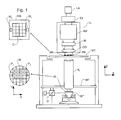
- Figure 1 schematically depicts a lithographic projection apparatus according to a particular embodiment of the invention.
- the apparatus comprises:
- the source LA e.g. an Hg lamp or excimer laser
- the source LA produces a beam of radiation.
- This beam is fed into an illumination system (illuminator) IL, either directly or after having traversed conditioning means, such as a beam expander Ex, for example.
- the illuminator IL may comprise adjusting means AM for setting the outer and/or inner radial extent (commonly referred to as ⁇ -outer and ⁇ -inner, respectively) of the intensity distribution in the beam.
- ⁇ -outer and ⁇ -inner commonly referred to as ⁇ -outer and ⁇ -inner, respectively
- it will generally comprise various other components, such as an integrator IN and a condenser CO.
- the beam PB impinging on the mask MA has a desired intensity distribution in its cross-section.
- the source LA may be within the housing of the lithographic projection apparatus (as is often the case when the source LA is a mercury lamp, for example), but that it may also be remote from the lithographic projection apparatus, the radiation beam which it produces being led into the apparatus (e.g. with the aid of suitable directing mirrors); this latter scenario is often the case when the source LA is an excimer laser.
- the current invention and Claims encompass both of these scenarios.
- the beam PB subsequently intercepts the mask MA, which is held on a mask table MT. Having traversed the mask MA, the beam PB passes through the lens PL, which focuses the beam PB onto a target portion C of the substrate W. With the aid of the second positioning means (and interferometric measuring means IF), the substrate table WT can be moved accurately, e.g . so as to position different target portions C in the path of the beam PB. Similarly, the first positioning means can be used to accurately position the mask MA with respect to the path of the beam PB, e.g . after mechanical retrieval of the mask MA from a mask library, or during a scan.
- the mask table MT may just be connected to a short stroke actuator, or may be fixed.
- the depicted apparatus can be used in two different modes:
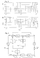
- Figure 2 depicts a control theory diagram of a control system used in an apparatus according to a first embodiment of the invention.
- the top loop represents the mask table (or reticle stage: RS), consisting of the mechanical transfer H RS and controller G RS .
- the bottom loop is the substrate table (or wafer stage: WS), consisting of the mechanical transfer H WS and controller G WS .
- the substrate table error e WS is added to the mask table setpoint SPR, and a WS acceleration error is generated.
- This error is combined with the output of the mask table controller G RS so that an extra force is generated which, when applied to the mask stage, should give it four times the acceleration of the WS.
- the mask table controller G RS would consider this force a disturbance, and would react and try to diminish the effect of the feedforward.
- the mask stage error e RS remains zero and hence the mask stage controller is left "unaware" of any extra force injection.
- the predictor 10 employs a prediction by sine-fit method which assumes a limited number of dominant frequencies in the signal to be predicted. Assume that the substrate table position error e WS consists of m sinusoids with unknown amplitude and phase, but with known frequencies:
- n 4
- a 1 , a 2 , b 1 , b 2 can be solved.
- every sample the above 4 ⁇ 4 matrix must be generated, inverted, and multiplied with the y-vector containing the last 4 samples of the data to be predicted.
- y ( t 0 ) a 1 sin(2 ⁇ f 1 t 0 ) + b 1 cos(2 ⁇ f 1 t 0 )+ a 2 sin(2 ⁇ f 2 t 0 )+ b 2 cos(2 ⁇ f 2 t 0 )
- a computationally more efficient way for the case that the matrix is square ( n 2m ), lies in a better choice of the time scale.
- the time scale is shifted such that at the prediction target time instant, t is defined as 0.
- the time scale hence shifts each sample.
- There is no reason to keep the time scale absolute, and in this case it is advantageous to shift it each sample such that the time instant of the predicted value coincides with t 0 on the time scale. In that case:
- Figures 3A and B show the magnitude and phase respectively of the frequency response of this predictor for various values of n.
- the chosen prediction frequencies f 1 and f 2 , amplitude and phase are always correct (prediction is exact).
- n 4 (minimum) the result is still good.
- the DC gain can be forced to 1 by adding a column vector containing 1's at the right side of the matrix A, and adding one offset coefficient c to the vector containing a and b coefficients.
- the signal y is then supposed to include a DC component: n must then be 2m+1 , minimum.
- the prediction horizon can have any value and is not restricted to whole number of samples. This is achieved by shifting the time scale.
- the predictor receives the substrate table position error and predicts its value one sample in the future based on the chosen prediction frequencies.
- the predictor is implemented as a 4 th -order FIR filter (two prediction frequencies + a DC component).
- the predictor output is refined in the frequency domain by one or more conventional filters depicted by the block 'H Filter '.
- the output of H Filter is filtered by low-pass filter 14, with a gain of -4, and added to the mask table setpoint SPR.
- the output of H Filter is double-differentiated, multiplied by the mask table mass m, filtered by a low-pass filter 16 which has the same characteristics as low-pass filter 14, and added to the mask table controller output.
- the predictor is used to predict the second derivative of y by evaluating: Hence, the only difference is the determination of the FIR filter parameters.
- Figures 7A and B show the response of the double-derivative predictor when making use of the same base frequencies as in the first embodiment: 107 and 185 Hz. It can be seen that below 107 Hz, the magnitude becomes flat, while a +2 slope is required. To repair this behavior, a very low frequency of 1 rad/s is included in the base frequencies, forcing a proper response for lower frequencies as also shown in Figures 7A and B. Introducing a DC gain of 0 does not help here, because this can also be obtained by a +1 slope. A low, nonzero extra base frequency is therefore required. The cost is, again, a larger high-frequency gain.
- Figure 8 shows the discrete poles and zeros of the FIR filter that results from this design technique.
- the sine-fit predictor creates three pole/zero pairs at strategic locations. Note that this filter has no continuous-time counterpart.
- the substrate table position error is fed through the block 'H Filter ', which refines the phase at specific frequencies present in the substrate table position error.
- the output of H Filter is filtered by low-pass filter 14, with a gain of -4, and added to the mask table setpoint SPR.
- the output of H Filter is fed to the acceleration error predictor, which predicts the substrate table acceleration error in the future.
- the predictor is implemented as a 5 th -order FIR filter (three prediction frequencies, of which one is kept very low to force a correct low-frequency behaviour).
- the predictor output is multiplied by the mask table mass m, filtered by a low-pass filter 16 which has the same characteristics as low-pass filter 14, and added to the mask table controller output.
- Figures 5A, 5B and 6 illustrate the improvement obtained with the predictor of the present invention.
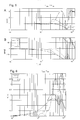
- Figures 5A and B show the magnitude and phase of the transfer function y rs /e ws for the prior art arrangement a) without optimal conventional filters (solid line), b) the prior art with optimal conventional filters (long dashed line) and c) the present embodiment (short dashed line).
- the feedthrough factor e WRS /e WS is shown in Figure 6.
- 0 is ideal whilst values below 1 denote improvement and values above 1 denote degradation.
- introduction of the prediction of the present invention improves the feedthrough factor at frequencies up to about 350 Hz compared to the prior art at the cost of some increase at higher frequencies, which are less important.
- results for moving average (MA) and moving standard deviation (MSD) are shown in the table, which also includes the best-obtained results using lead-lag filters only.
- MA-X [nm] MA-Y [nm]
- MSD-X [nm] MSD-Y [nm] e WS 8.7 20.2 20.9 31.3 e WRS , original 2.2 2.9 11.6 9.4 e WRS , lead-lag filters 1.9 2.3 8.1 7.5 e WRS , acc. predictor 1.5 1.9 6.8 6.3
- the sine-based predictor is replaced by a predictor based on a polynomial extrapolation of previous data points.
- n samples On the last n samples a polynomial can be fitted (having a maximum order of (n-1)), that can be used for extrapolation to the next sample.
- a basic example is shown in Figure 9.
- the last four samples are used to fit a straight line through, that is used to predict the next sample.
- FIGS. 10A and B show the frequency response for various values of n . It is seen that the 3rd-order polynomial is flat up to around 300 Hz, above which a large gain occurs. The larger the polynomial order, the better the phase advantage, but also the larger the high-frequency gain. This is true in general: a large phase advantage is combined with unfavorable high-frequency gain.
Landscapes
- Physics & Mathematics (AREA)
- General Physics & Mathematics (AREA)
- Exposure And Positioning Against Photoresist Photosensitive Materials (AREA)
- Exposure Of Semiconductors, Excluding Electron Or Ion Beam Exposure (AREA)
Priority Applications (1)
| Application Number | Priority Date | Filing Date | Title |
|---|---|---|---|
| EP02253926A EP1265106A3 (de) | 2001-06-06 | 2002-06-06 | Lithographischer Apparat und Verfahren zur Herstellung eines Artikels |
Applications Claiming Priority (3)
| Application Number | Priority Date | Filing Date | Title |
|---|---|---|---|
| EP01304950 | 2001-06-06 | ||
| EP01304950A EP1265104A1 (de) | 2001-06-06 | 2001-06-06 | Lithographischer Apparat, Verfahren zur Herstellung eines Artikels und dabei erzeugter Artikel |
| EP02253926A EP1265106A3 (de) | 2001-06-06 | 2002-06-06 | Lithographischer Apparat und Verfahren zur Herstellung eines Artikels |
Publications (2)
| Publication Number | Publication Date |
|---|---|
| EP1265106A2 true EP1265106A2 (de) | 2002-12-11 |
| EP1265106A3 EP1265106A3 (de) | 2005-01-05 |
Family
ID=26077136
Family Applications (1)
| Application Number | Title | Priority Date | Filing Date |
|---|---|---|---|
| EP02253926A Withdrawn EP1265106A3 (de) | 2001-06-06 | 2002-06-06 | Lithographischer Apparat und Verfahren zur Herstellung eines Artikels |
Country Status (1)
| Country | Link |
|---|---|
| EP (1) | EP1265106A3 (de) |
Cited By (2)
| Publication number | Priority date | Publication date | Assignee | Title |
|---|---|---|---|---|
| US7818073B2 (en) * | 2006-04-20 | 2010-10-19 | Asml Netherlands B.V. | Method for obtaining improved feedforward data, a lithographic apparatus for carrying out the method and a device manufacturing method |
| CN102087482A (zh) * | 2010-12-27 | 2011-06-08 | 中国科学院光电技术研究所 | 光刻机工件台同步运动误差校正控制系统 |
Family Cites Families (5)
| Publication number | Priority date | Publication date | Assignee | Title |
|---|---|---|---|---|
| JPH08293459A (ja) * | 1995-04-21 | 1996-11-05 | Nikon Corp | ステージ駆動制御方法及びその装置 |
| JP3352286B2 (ja) * | 1995-07-13 | 2002-12-03 | キヤノン株式会社 | 位置制御方法及び装置並びにそれを使用した半導体製造装置 |
| US5907392A (en) * | 1995-07-20 | 1999-05-25 | Nikon Corporation | Exposure apparatus |
| US5940789A (en) * | 1996-05-17 | 1999-08-17 | Nikon Corporation | Stage control method and apparatus with varying stage controller parameter |
| EP0967525B1 (de) * | 1998-06-23 | 2005-11-16 | ASML Netherlands B.V. | Lithographischer Projektionsapparat |
-
2002
- 2002-06-06 EP EP02253926A patent/EP1265106A3/de not_active Withdrawn
Cited By (3)
| Publication number | Priority date | Publication date | Assignee | Title |
|---|---|---|---|---|
| US7818073B2 (en) * | 2006-04-20 | 2010-10-19 | Asml Netherlands B.V. | Method for obtaining improved feedforward data, a lithographic apparatus for carrying out the method and a device manufacturing method |
| CN102087482A (zh) * | 2010-12-27 | 2011-06-08 | 中国科学院光电技术研究所 | 光刻机工件台同步运动误差校正控制系统 |
| CN102087482B (zh) * | 2010-12-27 | 2012-10-03 | 中国科学院光电技术研究所 | 光刻机工件台同步运动误差校正控制系统 |
Also Published As
| Publication number | Publication date |
|---|---|
| EP1265106A3 (de) | 2005-01-05 |
Similar Documents
| Publication | Publication Date | Title |
|---|---|---|
| US6727977B2 (en) | Lithographic apparatus, device manufacturing method, and device manufactured thereby | |
| EP1321822A1 (de) | Lithographischer Apparat und Verfahren zur Herstellung einer Vorrichtung | |
| US7126671B2 (en) | Lithographic apparatus and device manufacturing method | |
| US20020149754A1 (en) | Lithographic apparatus, device manufacturing method, and device manufacturing thereby | |
| US7209219B2 (en) | System for controlling a position of a mass | |
| EP2045664A2 (de) | Lithografische Vorrichtung, Projektionsanordnung und aktive Dämpfung | |
| US8384881B2 (en) | Lithographic apparatus, stage apparatus and device manufacturing method | |
| CN100507718C (zh) | 投影系统及利用该投影系统的方法 | |
| US7061587B2 (en) | Control system, lithographic apparatus, device manufacturing method, and device manufactured thereby | |
| JP3955837B2 (ja) | リソグラフィ機器およびデバイスの製造方法 | |
| US7256866B2 (en) | Lithographic apparatus and device manufacturing method | |
| EP1469348A1 (de) | Projektionssystem und Verfahren zu dessen Verwendung | |
| JP2007513503A (ja) | リソグラフィ装置及びデバイス製造方法 | |
| EP1383007A1 (de) | Lithographischer Apparat und Verfahren zur Herstellung einer Vorrichtung | |
| US7136148B2 (en) | Lithographic apparatus and device manufacturing method | |
| EP1265106A2 (de) | Lithographischer Apparat und Verfahren zur Herstellung eines Artikels | |
| EP1225482A1 (de) | Lithographischer Apparat und Verfahren zur Herstellung einer Vorrichtung | |
| US7847919B2 (en) | Lithographic apparatus having feedthrough control system | |
| US7352436B2 (en) | Lithographic apparatus, projection apparatus and device manufacturing method | |
| EP1465015A1 (de) | Lithographischer Apparat und Verfahren zur Herstellung einer Vorrichtung | |
| EP1380899B1 (de) | Lithographischer Apparat und Verfahren zur Herstellung einer Vorrichtung | |
| EP1271248A1 (de) | Lithographischer Apparat | |
| EP1480093A1 (de) | Steuerungssystem, lithographisches Gerät, Verfahren zur Herstellung eines Gerätes und hiermit hergestelltes Gerät | |
| EP1385058A1 (de) | Lithographischer Apparat und Verfahren zur Herstellung einer Vorrichtung | |
| EP1318431A1 (de) | Lithographischer Apparat, Verfahren zur Herstellung einer Vorrichtung, und Verfahren zur Herstellung eines optischen Elementes |
Legal Events
| Date | Code | Title | Description |
|---|---|---|---|
| PUAI | Public reference made under article 153(3) epc to a published international application that has entered the european phase |
Free format text: ORIGINAL CODE: 0009012 |
|
| AK | Designated contracting states |
Kind code of ref document: A2 Designated state(s): AT BE CH CY DE DK ES FI FR GB GR IE IT LI LU MC NL PT SE TR |
|
| AX | Request for extension of the european patent |
Free format text: AL;LT;LV;MK;RO;SI |
|
| RAP1 | Party data changed (applicant data changed or rights of an application transferred) |
Owner name: ASML NETHERLANDS B.V. |
|
| PUAL | Search report despatched |
Free format text: ORIGINAL CODE: 0009013 |
|
| AK | Designated contracting states |
Kind code of ref document: A3 Designated state(s): AT BE CH CY DE DK ES FI FR GB GR IE IT LI LU MC NL PT SE TR |
|
| AX | Request for extension of the european patent |
Extension state: AL LT LV MK RO SI |
|
| 17P | Request for examination filed |
Effective date: 20050217 |
|
| 17Q | First examination report despatched |
Effective date: 20050502 |
|
| AKX | Designation fees paid |
Designated state(s): DE FR GB IT NL |
|
| 17Q | First examination report despatched |
Effective date: 20050502 |
|
| STAA | Information on the status of an ep patent application or granted ep patent |
Free format text: STATUS: THE APPLICATION IS DEEMED TO BE WITHDRAWN |
|
| 18D | Application deemed to be withdrawn |
Effective date: 20091016 |