EP1265362A1 - Tristate-Multiplexer - Google Patents
Tristate-Multiplexer Download PDFInfo
- Publication number
- EP1265362A1 EP1265362A1 EP02253334A EP02253334A EP1265362A1 EP 1265362 A1 EP1265362 A1 EP 1265362A1 EP 02253334 A EP02253334 A EP 02253334A EP 02253334 A EP02253334 A EP 02253334A EP 1265362 A1 EP1265362 A1 EP 1265362A1
- Authority
- EP
- European Patent Office
- Prior art keywords
- select signal
- terminal
- data input
- circuit
- channel transistor
- Prior art date
- Legal status (The legal status is an assumption and is not a legal conclusion. Google has not performed a legal analysis and makes no representation as to the accuracy of the status listed.)
- Granted
Links
- 238000000034 method Methods 0.000 claims description 5
- 238000010586 diagram Methods 0.000 description 6
- 230000003068 static effect Effects 0.000 description 6
- 238000012986 modification Methods 0.000 description 5
- 230000004048 modification Effects 0.000 description 5
- 238000007599 discharging Methods 0.000 description 4
- 238000007792 addition Methods 0.000 description 2
- 230000003213 activating effect Effects 0.000 description 1
- 238000013459 approach Methods 0.000 description 1
- 230000001419 dependent effect Effects 0.000 description 1
- 238000005516 engineering process Methods 0.000 description 1
- 229910044991 metal oxide Inorganic materials 0.000 description 1
- 150000004706 metal oxides Chemical class 0.000 description 1
- 239000004065 semiconductor Substances 0.000 description 1
- 230000001360 synchronised effect Effects 0.000 description 1
Images


Classifications
-
- H—ELECTRICITY
- H03—ELECTRONIC CIRCUITRY
- H03K—PULSE TECHNIQUE
- H03K17/00—Electronic switching or gating, i.e. not by contact-making and –breaking
- H03K17/51—Electronic switching or gating, i.e. not by contact-making and –breaking characterised by the components used
- H03K17/56—Electronic switching or gating, i.e. not by contact-making and –breaking characterised by the components used by the use, as active elements, of semiconductor devices
- H03K17/687—Electronic switching or gating, i.e. not by contact-making and –breaking characterised by the components used by the use, as active elements, of semiconductor devices the devices being field-effect transistors
- H03K17/693—Switching arrangements with several input- or output-terminals, e.g. multiplexers, distributors
-
- H—ELECTRICITY
- H03—ELECTRONIC CIRCUITRY
- H03K—PULSE TECHNIQUE
- H03K17/00—Electronic switching or gating, i.e. not by contact-making and –breaking
- H03K17/002—Switching arrangements with several input- or output terminals
- H03K17/005—Switching arrangements with several input- or output terminals with several inputs only
Definitions
- This invention relates to complimentary metal oxide semiconductor (CMOS) circuit designs, and more particularly, but not exclusively, to multiplexer designs.
- CMOS complimentary metal oxide semiconductor
- CMOS multiplexer functions may typically be implemented using two or more stages of logic (e.g. a complex gate such as an and / or function). Each stage represents a gate delay to the input data. This means that the traditional static CMOS multiplexer may be slow. This may be especially true for multiple input multiplexers.
- stages of logic e.g. a complex gate such as an and / or function.
- pre-charge logic is typically used to charge an output node to a binary one, and then if the output data is a binary zero, evaluating logic pulls the output node low.
- the pre-charging circuitry reduces the need for multiple logic stages used in static CMOS designs. Thus pre-charging may allow for a faster output response time.
- some CMOS multiplexer designs may require a large P-Channel load device per stage, which may have a large capacitance associated with it.
- CMOS multiplexer may be the only choice. Accordingly, it is desirable to have a faster multiple input static CMOS multiplexer design.
- a multiplexer circuit may be configured to receive at least a first data input and a second data input, which are selected by at least a first select signal and a second select signal, respectively.
- a first circuit is configured to provide an output to an output node responsive to the data input that is selected by the corresponding select signal being active.
- the multiplexer circuit may further use a tristate circuit, which is also coupled to receive the first select signal and the second select signal. If neither the first select signal nor the second select signal are active, then the tristate circuit is configured to prevent the first circuit from providing an output to the output node.
- the multiplexer circuit may be used to build larger multiplexers by instantiating the multiplexer circuit multiple times.
- a multiplexer circuit comprising a first circuit coupled to receive at least a first data input and a second data input.
- the first circuit is also coupled to receive at least a first select signal and a second select signal corresponding to the first data input and the second data input, respectively.
- the first circuit is coupled to an output node and is configured to provide an output on the output node responsive to a corresponding one of the first select signal or the second select signal being active.
- the multiplexer circuit may also include a tristate circuit coupled to receive the first select signal and the second select signal.
- the tristate circuit is also coupled to the first circuit.
- the tristate circuit is configured to prevent the first circuit from providing an output on the output node responsive to the first select signal and the second select signal being inactive.
- a multiplexer circuit comprising a first multiplexer circuit is coupled to a first data input and a second data input.
- the first multiplexer circuit is also coupled to a first select signal and a second select signal corresponding to the first data input and the second data input, respectively.
- the first multiplexer circuit is configured to provide an output on an output node responsive to a corresponding one of the first select signal or the second select signal being active and to provide no output on the output node responsive to the first select signal and the second select signal being inactive.
- the multiplexer circuit may also include a second multiplexer circuit coupled to a third data input and a fourth data input.
- the second multiplexer circuit is also coupled to a third select signal and a fourth select signal corresponding to the third data input and the fourth data input, respectively.
- the second multiplexer circuit is configured to provide an output on the output node responsive to a corresponding one of the third select signal or the fourth select signal being active and to provide no output on the output node responsive to the first select signal and the second select signal being inactive.
- a method of operating a multiplexer circuit is contemplated.
- at least a first data input and a second data input are received by the multiplexer circuit.
- at least a first select signal corresponding to the first data input and a second select signal corresponding to the second data input are also received by the multiplexer circuit.
- the multiplexer circuit provides an output on an output node responsive to a corresponding one of the first select signal or the second select signal being active.
- the multiplexer provides no output on the output node responsive to the first select signal and the second select signal being inactive.
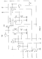
- FIG. 1 a circuit diagram of one embodiment of a two input multiplexer is shown.
- the multiplexer circuit illustrated in FIG. 1 includes ten transistors, four of which are P-channel CMOS transistors and six are N-channel CMOS transistors.
- a P-channel transistor T1 is connected in series with another P-channel transistor T2.
- One end of the series connection is connected to a positive power supply voltage VDD.
- the other end of the series connection is connected to the gate terminal of a P-channel transistor T10.
- the gate terminal of transistor T1 is connected to select signal s0 and the gate of transistor T2 is connected to select signal s1.
- the select signals s0 and s1 are also connected to the gates of an N-channel transistor T4 and an N-channel transistor T3, respectively.
- Transistors T3 and T4 are connected in parallel such that their output terminals are connected together.
- the input terminal of transistor T4 is connected to a data input signal d0 and the input terminal of transistor T3 is connected to a data input signal d1.
- An N-channel transistor T5 is connected in series with an N-channel transistor T6.
- An N-channel transistor T7 is connected in series with an N-channel transistor T8.
- the two series pairs of transistors are connected in parallel such that the output of transistor T5 and the output of transistor T7 are connected together. This connection is an output node 10.
- the other ends of the series connections are both connected to a circuit ground GND.
- the gate terminal of transistor T5 is connected to select signal s0 and the gate terminal of transistor T7 is connected to select signal s1.
- the gate terminal of transistor T6 is connected to data input signal d0 and the gate terminal of transistor T8 is connected to data input signal d1.
- One terminal of transistor T10 is connected to VDD, while the other terminal is connected to output node 10.
- Output node 10 is also connected to the gate terminal of a P-channel transistor T9.
- One terminal of transistor T9 is connected to VDD while the other terminal is connected to the gate of transistor T10.
- Output node 10 may also be connected to a data bus d_bus 50.
- the multiplexer circuit may be thought of as having two main sub-circuits: a charge and discharge circuit 15 and a tristate circuit 5.
- Charge and discharge circuit 15 is configured to charge or discharge output node 10 (thus providing a binary one or binary zero output, respectively) responsive to an active select signal and the data on the corresponding data signal. More particularly, charge and discharge circuit 15 may charge the output node 10 (providing a binary one) responsive to a selected data input being binary zero, and may discharge the output node 10 (providing a binary zero) responsive to a selected data input being a binary one.
- charge and discharge circuit 15 may provide an inverting multiplexing function. Other embodiments may provide a non-inverting multiplexing function.
- charge and discharge circuit 15 may include two subcircuits: A charging circuit 25 that includes transistors T3, T4, T9 and T10 and a discharging circuit 35 that includes transistors T5, T6, T7 and T8.
- Charging circuit 25 charges output node 10 to VDD (a binary one) responsive to data present on the data input if the corresponding select signal is active. More particularly, charging circuit 25 charges output node 10 responsive to a binary zero on the selected data input.
- Discharging circuit 35 discharges output node 10 to GND (a binary zero) responsive to data present on the data input if the corresponding select signal is active. More particularly, discharging circuit 35 discharges output node 10 responsive to a binary one on the selected data input.
- Tristate circuit 5 includes transistor T1 and transistor T2. Tristate circuit 5 prevents charge and discharge circuit 15 from providing on output on output node 10 if neither of the select signals are active. More particularly in the illustrated embodiment, tristate circuit 5 causes VDD to be applied to the gate of transistor T10 when neither of the select signals are active. Thus, transistor T10 is off. When neither select signal is active, the series transistor connections T5/T6 and T7/T8 are off as well, preventing discharge of the output node 10. Accordingly, output node 10 may be floating when neither of the select signals are active.
- FIG. 1 is shown using CMOS transistors. It is contemplated that other embodiments may use any suitable set of transistors that may be manufactured in technologies other than CMOS.
- this embodiment illustrates a two input multiplexer.
- This particular embodiment has two select signals s0 and s1 that control which data input is selected as the output. One of the data input signals is selected by activating the corresponding select line.
- an active signal refers to a binary one
- an inactive signal refers to a binary zero.
- an active signal may be a binary zero
- an inactive signal may be a binary one.
- this embodiment illustrates a two input multiplexer, it is contemplated that other embodiments may be N input multiplexers. For example, a four input multiplexer is illustrated below.
- the binary zero on data input d0 is applied to the gate of transistor T6, which is therefore off. Accordingly, the series connection of transistors T5 and T6 does not discharge output node 10. Since transistor T4 is on, the binary zero on data input d0 is passed through transistor T4 to the gate of transistor T10, causing it to turn on. Transistor T10 charges output node 10 (and therefore d_bus 50) to VDD. Thus the binary zero input on data input d0 is inverted and a binary one is present at output node 10.
- the multiplexer is an inverting multiplexer. Other embodiments may be non-inverting, (e.g. by adding an inverting stage at output node 10).
- the binary one on output node 10 is also applied to the gate of transistor T9, which is therefore off.
- FIG. 2 a circuit diagram of one embodiment of a four input multiplexer circuit is illustrated.
- the four input multiplexer shown in FIG. 2 includes a first two input multiplexer circuit, multiplexer 1 and a second two input multiplexer, multiplexer 2.
- the output nodes of multiplexer 1 and multiplexer 2 are connected in parallel such that an output node 10 of multiplexer 1 and an output node 20 of multiplexer 2 are both connected to d_bus 50.
- the four data input signals are d0, d1, d2, d3 and the four corresponding select signals are s0, s1, s2, s3, respectively.
- Both multiplexer 1 and multiplexer 2 are instantiations of the multiplexer circuit of FIG.1.
- the tristate circuit described above in the description of FIG. 1 enables multiple two input multiplexers to be connected to a common output node by causing each multiplexer output node to be placed in a high impedance state when neither of the respective multiplexer select lines is active. For example, in FIG. 2, if select signal s2 is active, then s0, s1 and s3 are inactive. This places output node 10 of multiplexer 1 in a high impedance state allowing multiplexer 2 to drive data onto d_bus 50 without bus contention.
- the high impedance state of the inactive multiplexer allows the basic two input multiplexer of FIG. 1 to be instantiated N times to produce a 2N input multiplexer.
- the ability to instantiate the basic multiplexer may also provide circuit layout efficiency.
- FIG. 3 a circuit diagram of an alternative embodiment of a four input multiplexer circuit is shown.
- the four input multiplexer circuit of FIG. 3 is similar in operation to that of the two input multiplexer circuit described in FIG. 1 with the addition of two select signals s2 and s3, two data input signals d2 and d3 and some additional transistors to accommodate the additional input signals.
- P-channel transistors T1, T2 are connected in series and turn off P-channel transistor T10 in the event that neither input signal s0 nor s1 is active.
- P-channel transistors T3 and T4 are added in series with transistors T1 and T2.
- the four series transistors turn off P-channel transistor T18 when none of the four select signals s0, s1, s2 or s3 is active.
- Transistor T17 performs the same function as transistor T9 in FIG. 1.
- N-channel Transistors T5 and T6 of FIG. 3 perform the same operation as transistors N-channel T3 and T4 in FIG. 1.
- N-channel transistors T7, T8, T9 and T10 of FIG. 3 perform the same operation as N-channel transistors T5-T8 of FIG. 1.
- N-channel transistors T11-T14 of FIG. 3 perform a similar operation to that of transistors T7-T9, but they are responsive to data input signals d2 and d3 and select signals s2 and s3.
- N-channel transistors T15 and T16 perform a similar operation to that of transistors T5 and T6, but they are responsive to data input signals d2 and d3 and select signals s2 and s3.
- the four input multiplexer of FIG. 3 may also be instantiated N times to construct a 4N input multiplexer circuit by connecting the output nodes of each of the four input multiplexers together.
Landscapes
- Electronic Switches (AREA)
Applications Claiming Priority (2)
| Application Number | Priority Date | Filing Date | Title |
|---|---|---|---|
| US859194 | 2001-05-15 | ||
| US09/859,194 US6943589B2 (en) | 2001-05-15 | 2001-05-15 | Combination multiplexer and tristate driver circuit |
Publications (2)
| Publication Number | Publication Date |
|---|---|
| EP1265362A1 true EP1265362A1 (de) | 2002-12-11 |
| EP1265362B1 EP1265362B1 (de) | 2006-04-26 |
Family
ID=25330313
Family Applications (1)
| Application Number | Title | Priority Date | Filing Date |
|---|---|---|---|
| EP02253334A Expired - Lifetime EP1265362B1 (de) | 2001-05-15 | 2002-05-14 | Tristate-Multiplexer |
Country Status (3)
| Country | Link |
|---|---|
| US (1) | US6943589B2 (de) |
| EP (1) | EP1265362B1 (de) |
| DE (1) | DE60210865T2 (de) |
Families Citing this family (6)
| Publication number | Priority date | Publication date | Assignee | Title |
|---|---|---|---|---|
| US7230856B1 (en) * | 2004-12-22 | 2007-06-12 | Cypress Semiconductor Corporation | High-speed multiplexer latch |
| US7365569B1 (en) | 2005-05-26 | 2008-04-29 | Cypress Semiconductor Corporation | High-speed level shifter |
| US7710153B1 (en) * | 2006-06-30 | 2010-05-04 | Masleid Robert P | Cross point switch |
| US20140247720A1 (en) * | 2013-03-01 | 2014-09-04 | Nxp B.V. | Signal path isolation for conductive circuit paths and multipurpose interfaces |
| US9705504B1 (en) | 2016-01-13 | 2017-07-11 | Altera Corporation | Power gated lookup table circuitry |
| CN111984575B (zh) * | 2019-05-24 | 2021-12-17 | 瑞昱半导体股份有限公司 | 信号传输电路与方法 |
Citations (5)
| Publication number | Priority date | Publication date | Assignee | Title |
|---|---|---|---|---|
| JPH03125207A (ja) * | 1989-10-11 | 1991-05-28 | Seiko Epson Corp | クロック切り替え装置 |
| JPH04178011A (ja) * | 1990-11-13 | 1992-06-25 | Nec Corp | セレクタ |
| JPH0594549A (ja) * | 1991-09-30 | 1993-04-16 | Mitsubishi Electric Corp | 入出力回路 |
| US5438295A (en) * | 1993-06-11 | 1995-08-01 | Altera Corporation | Look-up table using multi-level decode |
| US6239646B1 (en) * | 1998-10-29 | 2001-05-29 | Cypress Semiconductor Corp. | High-speed, multiple-input multiplexer scheme |
Family Cites Families (15)
| Publication number | Priority date | Publication date | Assignee | Title |
|---|---|---|---|---|
| US3654394A (en) | 1969-07-08 | 1972-04-04 | Gordon Eng Co | Field effect transistor switch, particularly for multiplexing |
| US5012126A (en) * | 1990-06-04 | 1991-04-30 | Motorola, Inc. | High speed CMOS multiplexer having reduced propagation delay |
| US5243599A (en) | 1991-06-05 | 1993-09-07 | International Business Machines Corporation | Tree-type multiplexers and methods for configuring the same |
| US5646558A (en) | 1995-09-27 | 1997-07-08 | Intel Corporation | Plurality of distinct multiplexers that operate as a single multiplexer |
| US5789966A (en) | 1996-09-18 | 1998-08-04 | International Business Machines Corporation | Distributed multiplexer |
| US5920202A (en) | 1997-02-26 | 1999-07-06 | Xilinx, Inc. | Configurable logic element with ability to evaluate five and six input functions |
| JP3396720B2 (ja) | 1997-11-06 | 2003-04-14 | 株式会社リコー | 部分積生成回路 |
| US6081135A (en) | 1998-05-07 | 2000-06-27 | International Business Machines Corporation | Device and method to reduce power consumption in integrated semiconductor devices |
| US6087855A (en) * | 1998-06-15 | 2000-07-11 | International Business Machines Corporation | High performance dynamic multiplexers without clocked NFET |
| US6118300A (en) | 1998-11-24 | 2000-09-12 | Xilinx, Inc. | Method for implementing large multiplexers with FPGA lookup tables |
| US6819141B1 (en) * | 2000-03-14 | 2004-11-16 | International Business Machines Corporation | High speed, static digital multiplexer |
| US6522189B1 (en) | 2000-10-02 | 2003-02-18 | Broadcom Corporation | High-speed bank select multiplexer latch |
| US6388466B1 (en) | 2001-04-27 | 2002-05-14 | Xilinx, Inc. | FPGA logic element with variable-length shift register capability |
| US6556042B1 (en) | 2002-02-20 | 2003-04-29 | Xilinx, Inc. | FPGA with improved structure for implementing large multiplexers |
| US6674671B1 (en) | 2002-08-14 | 2004-01-06 | Broadcom Corp. | Circuit for lines with multiple drivers |
-
2001
- 2001-05-15 US US09/859,194 patent/US6943589B2/en not_active Expired - Fee Related
-
2002
- 2002-05-14 DE DE60210865T patent/DE60210865T2/de not_active Expired - Lifetime
- 2002-05-14 EP EP02253334A patent/EP1265362B1/de not_active Expired - Lifetime
Patent Citations (5)
| Publication number | Priority date | Publication date | Assignee | Title |
|---|---|---|---|---|
| JPH03125207A (ja) * | 1989-10-11 | 1991-05-28 | Seiko Epson Corp | クロック切り替え装置 |
| JPH04178011A (ja) * | 1990-11-13 | 1992-06-25 | Nec Corp | セレクタ |
| JPH0594549A (ja) * | 1991-09-30 | 1993-04-16 | Mitsubishi Electric Corp | 入出力回路 |
| US5438295A (en) * | 1993-06-11 | 1995-08-01 | Altera Corporation | Look-up table using multi-level decode |
| US6239646B1 (en) * | 1998-10-29 | 2001-05-29 | Cypress Semiconductor Corp. | High-speed, multiple-input multiplexer scheme |
Non-Patent Citations (3)
| Title |
|---|
| PATENT ABSTRACTS OF JAPAN vol. 015, no. 338 (P - 1243) 27 August 1991 (1991-08-27) * |
| PATENT ABSTRACTS OF JAPAN vol. 016, no. 486 (E - 1276) 8 October 1992 (1992-10-08) * |
| PATENT ABSTRACTS OF JAPAN vol. 017, no. 445 (P - 1593) 16 August 1993 (1993-08-16) * |
Also Published As
| Publication number | Publication date |
|---|---|
| EP1265362B1 (de) | 2006-04-26 |
| DE60210865T2 (de) | 2006-11-09 |
| US6943589B2 (en) | 2005-09-13 |
| DE60210865D1 (de) | 2006-06-01 |
| US20020172232A1 (en) | 2002-11-21 |
Similar Documents
| Publication | Publication Date | Title |
|---|---|---|
| US6972599B2 (en) | Pseudo CMOS dynamic logic with delayed clocks | |
| CN1143434C (zh) | 用于脉冲输入的高速率的cmos逻辑结构 | |
| US20040257115A1 (en) | N-domino output latch with accelerated evaluate path | |
| US8030969B2 (en) | Semiconductor integrated circuit | |
| JP3555080B2 (ja) | 汎用ロジックモジュール及びこれを用いたセル | |
| US5986466A (en) | Programmable gate array | |
| US6094072A (en) | Methods and apparatus for bipolar elimination in silicon-on-insulator (SOI) domino circuits | |
| US5546035A (en) | Latch circuit having a logical operation function | |
| US6943589B2 (en) | Combination multiplexer and tristate driver circuit | |
| US5663669A (en) | Circuitry and method for latching information | |
| US6407585B1 (en) | Method and apparatus for a family of self clocked dynamic circuits | |
| US6437602B1 (en) | Fully dynamic logic network circuits | |
| US6211702B1 (en) | Input circuit | |
| US5818264A (en) | Dynamic circuit having improved noise immunity and method therefor | |
| EP0846372B1 (de) | Schnelle cmos pufferschaltung | |
| US6005418A (en) | Low power consuming logic circuit | |
| US5894227A (en) | Level restoration circuit for pass logic devices | |
| JPH06224730A (ja) | 出力バッファ回路 | |
| WO2009063527A2 (en) | Logic gate with a reduced number of switches, especially for applications in integrated circuits | |
| US6040717A (en) | FRCPG: Forecasted restoration complementary pass gates | |
| US5936427A (en) | Three-input exclusive NOR circuit | |
| US20030001622A1 (en) | Symmetric differential domino "AND gate" | |
| US6731137B1 (en) | Programmable, staged, bus hold and weak pull-up for bi-directional I/O | |
| US6794903B2 (en) | CMOS parallel dynamic logic and speed enhanced static logic | |
| EP0821484B1 (de) | Hohen Spannungen widerstehende Ausgangsstufe |
Legal Events
| Date | Code | Title | Description |
|---|---|---|---|
| PUAI | Public reference made under article 153(3) epc to a published international application that has entered the european phase |
Free format text: ORIGINAL CODE: 0009012 |
|
| 17P | Request for examination filed |
Effective date: 20020611 |
|
| AK | Designated contracting states |
Kind code of ref document: A1 Designated state(s): AT BE CH CY DE DK ES FI FR GB GR IE IT LI LU MC NL PT SE TR |
|
| AX | Request for extension of the european patent |
Free format text: AL;LT;LV;MK;RO;SI |
|
| AKX | Designation fees paid |
Designated state(s): DE FR GB |
|
| 17Q | First examination report despatched |
Effective date: 20040617 |
|
| GRAP | Despatch of communication of intention to grant a patent |
Free format text: ORIGINAL CODE: EPIDOSNIGR1 |
|
| GRAS | Grant fee paid |
Free format text: ORIGINAL CODE: EPIDOSNIGR3 |
|
| GRAA | (expected) grant |
Free format text: ORIGINAL CODE: 0009210 |
|
| AK | Designated contracting states |
Kind code of ref document: B1 Designated state(s): DE FR GB |
|
| REG | Reference to a national code |
Ref country code: GB Ref legal event code: FG4D |
|
| REF | Corresponds to: |
Ref document number: 60210865 Country of ref document: DE Date of ref document: 20060601 Kind code of ref document: P |
|
| ET | Fr: translation filed | ||
| PLBE | No opposition filed within time limit |
Free format text: ORIGINAL CODE: 0009261 |
|
| STAA | Information on the status of an ep patent application or granted ep patent |
Free format text: STATUS: NO OPPOSITION FILED WITHIN TIME LIMIT |
|
| 26N | No opposition filed |
Effective date: 20070129 |
|
| REG | Reference to a national code |
Ref country code: FR Ref legal event code: CA |
|
| PGFP | Annual fee paid to national office [announced via postgrant information from national office to epo] |
Ref country code: GB Payment date: 20130522 Year of fee payment: 12 |
|
| PGFP | Annual fee paid to national office [announced via postgrant information from national office to epo] |
Ref country code: FR Payment date: 20130604 Year of fee payment: 12 |
|
| PGFP | Annual fee paid to national office [announced via postgrant information from national office to epo] |
Ref country code: DE Payment date: 20140531 Year of fee payment: 13 |
|
| REG | Reference to a national code |
Ref country code: DE Ref legal event code: R119 Ref document number: 60210865 Country of ref document: DE |
|
| GBPC | Gb: european patent ceased through non-payment of renewal fee |
Effective date: 20140514 |
|
| REG | Reference to a national code |
Ref country code: FR Ref legal event code: ST Effective date: 20150130 |
|
| PG25 | Lapsed in a contracting state [announced via postgrant information from national office to epo] |
Ref country code: FR Free format text: LAPSE BECAUSE OF NON-PAYMENT OF DUE FEES Effective date: 20140602 Ref country code: GB Free format text: LAPSE BECAUSE OF NON-PAYMENT OF DUE FEES Effective date: 20140514 |
|
| PG25 | Lapsed in a contracting state [announced via postgrant information from national office to epo] |
Ref country code: DE Free format text: LAPSE BECAUSE OF NON-PAYMENT OF DUE FEES Effective date: 20141202 |