EP1280205A2 - Halbleiter-Speicherbauteil - Google Patents
Halbleiter-Speicherbauteil Download PDFInfo
- Publication number
- EP1280205A2 EP1280205A2 EP01123208A EP01123208A EP1280205A2 EP 1280205 A2 EP1280205 A2 EP 1280205A2 EP 01123208 A EP01123208 A EP 01123208A EP 01123208 A EP01123208 A EP 01123208A EP 1280205 A2 EP1280205 A2 EP 1280205A2
- Authority
- EP
- European Patent Office
- Prior art keywords
- channel body
- memory device
- gate
- semiconductor memory
- semiconductor
- Prior art date
- Legal status (The legal status is an assumption and is not a legal conclusion. Google has not performed a legal analysis and makes no representation as to the accuracy of the status listed.)
- Withdrawn
Links
Images


Classifications
-
- H—ELECTRICITY
- H10—SEMICONDUCTOR DEVICES; ELECTRIC SOLID-STATE DEVICES NOT OTHERWISE PROVIDED FOR
- H10B—ELECTRONIC MEMORY DEVICES
- H10B12/00—Dynamic random access memory [DRAM] devices
- H10B12/20—DRAM devices comprising floating-body transistors, e.g. floating-body cells
-
- G—PHYSICS
- G11—INFORMATION STORAGE
- G11C—STATIC STORES
- G11C29/00—Checking stores for correct operation ; Subsequent repair; Testing stores during standby or offline operation
- G11C29/02—Detection or location of defective auxiliary circuits, e.g. defective refresh counters
-
- G—PHYSICS
- G11—INFORMATION STORAGE
- G11C—STATIC STORES
- G11C29/00—Checking stores for correct operation ; Subsequent repair; Testing stores during standby or offline operation
- G11C29/02—Detection or location of defective auxiliary circuits, e.g. defective refresh counters
- G11C29/021—Detection or location of defective auxiliary circuits, e.g. defective refresh counters in voltage or current generators
-
- G—PHYSICS
- G11—INFORMATION STORAGE
- G11C—STATIC STORES
- G11C29/00—Checking stores for correct operation ; Subsequent repair; Testing stores during standby or offline operation
- G11C29/02—Detection or location of defective auxiliary circuits, e.g. defective refresh counters
- G11C29/028—Detection or location of defective auxiliary circuits, e.g. defective refresh counters with adaption or trimming of parameters
-
- H—ELECTRICITY
- H10—SEMICONDUCTOR DEVICES; ELECTRIC SOLID-STATE DEVICES NOT OTHERWISE PROVIDED FOR
- H10B—ELECTRONIC MEMORY DEVICES
- H10B12/00—Dynamic random access memory [DRAM] devices
-
- H—ELECTRICITY
- H10—SEMICONDUCTOR DEVICES; ELECTRIC SOLID-STATE DEVICES NOT OTHERWISE PROVIDED FOR
- H10B—ELECTRONIC MEMORY DEVICES
- H10B12/00—Dynamic random access memory [DRAM] devices
- H10B12/30—DRAM devices comprising one-transistor - one-capacitor [1T-1C] memory cells
- H10B12/33—DRAM devices comprising one-transistor - one-capacitor [1T-1C] memory cells the capacitor extending under the transistor
-
- H—ELECTRICITY
- H10—SEMICONDUCTOR DEVICES; ELECTRIC SOLID-STATE DEVICES NOT OTHERWISE PROVIDED FOR
- H10B—ELECTRONIC MEMORY DEVICES
- H10B12/00—Dynamic random access memory [DRAM] devices
- H10B12/30—DRAM devices comprising one-transistor - one-capacitor [1T-1C] memory cells
- H10B12/34—DRAM devices comprising one-transistor - one-capacitor [1T-1C] memory cells the transistor being at least partially in a trench in the substrate
-
- H—ELECTRICITY
- H10—SEMICONDUCTOR DEVICES; ELECTRIC SOLID-STATE DEVICES NOT OTHERWISE PROVIDED FOR
- H10B—ELECTRONIC MEMORY DEVICES
- H10B12/00—Dynamic random access memory [DRAM] devices
- H10B12/50—Peripheral circuit region structures
-
- H—ELECTRICITY
- H10—SEMICONDUCTOR DEVICES; ELECTRIC SOLID-STATE DEVICES NOT OTHERWISE PROVIDED FOR
- H10D—INORGANIC ELECTRIC SEMICONDUCTOR DEVICES
- H10D30/00—Field-effect transistors [FET]
- H10D30/60—Insulated-gate field-effect transistors [IGFET]
- H10D30/711—Insulated-gate field-effect transistors [IGFET] having floating bodies
-
- H—ELECTRICITY
- H10—SEMICONDUCTOR DEVICES; ELECTRIC SOLID-STATE DEVICES NOT OTHERWISE PROVIDED FOR
- H10D—INORGANIC ELECTRIC SEMICONDUCTOR DEVICES
- H10D86/00—Integrated devices formed in or on insulating or conducting substrates, e.g. formed in silicon-on-insulator [SOI] substrates or on stainless steel or glass substrates
- H10D86/201—Integrated devices formed in or on insulating or conducting substrates, e.g. formed in silicon-on-insulator [SOI] substrates or on stainless steel or glass substrates the substrates comprising an insulating layer on a semiconductor body, e.g. SOI
-
- G—PHYSICS
- G11—INFORMATION STORAGE
- G11C—STATIC STORES
- G11C29/00—Checking stores for correct operation ; Subsequent repair; Testing stores during standby or offline operation
- G11C29/04—Detection or location of defective memory elements, e.g. cell constructio details, timing of test signals
- G11C29/08—Functional testing, e.g. testing during refresh, power-on self testing [POST] or distributed testing
- G11C29/12—Built-in arrangements for testing, e.g. built-in self testing [BIST] or interconnection details
- G11C2029/1202—Word line control
Definitions
- the present invention relates to a semiconductor memory device, specifically, to a semiconductor memory device having full depletion type MISFETs.
- a memory cell is composed of an MOS transistor and a capacitor.
- the scale-down of the DRAM has been remarkably advanced by the adoption of a trench capacitor structure and a stacked capacitor structure.
- F is a minimum feature size.
- the minimum feature size F decreases with the advance of generation, and when the cell size is generally taken to be ⁇ F 2 , a coefficient ⁇ also decreases with the advance of generation.
- a memory cell in the document (1) is composed of MOS transistors, each of which has a buried channel structure. Charge and discharge to/from a surface inversion layer is performed using a parasitic transistor formed at a taper portion of an element isolation insulating film to perform binary storage.
- a memory cell in the document (2) uses MOS transistors which are well-isolated from each other and uses a threshold voltage of the MOS transistor fixed by a well potential as binary data.
- a memory cell in the document (3) is composed of MOS transistors on an SOI substrate.
- a large negative voltage is applied from the SOI substrate side, and by utilizing accumulation of holes in an oxide film of a silicon layer and an interface, binary storage is performed by emitting and injecting these holes.
- a memory cell in the document (4) is composed of MOS transistors on an SOI substrate.
- the MOS transistor is one in terms of structure, but here a structure, in which a reverse conduction-type layer is formed on top of the surface of a drain diffusion region, whereby a P-MOS transistor for write and an N-MOS transistor for read are substantially combined integrally, is adopted. With a substrate region of the N-MOS transistor as a floating node, binary data are stored by its potential.
- the structure is complicated and the parasitic transistor is used, whereby there is a disadvantage in the controllability of its characteristic.
- the structure is simple, but it is necessary to control potential by connecting both a drain and a source of the transistor to a signal line.
- the cell size is large and rewrite bit by bit is impossible because of the well isolation.
- a potential control from the SOI substrate side is needed, and hence the rewrite bit by bit is impossible, whereby there is a difficulty in controllability.
- a special transistor structure is needed, and the memory cell requires a word line, a write bit line, a read bit line, and a purge line, whereby the number of signal lines increases.
- a partial depletion type MISFET when a voltage is applied to a gate to form a channel, a channel body is partially depleted and an electric neutral region remains therein.
- a MISFET is referred to as a PD-type MISFET hereinafter.
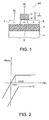
- Fig. 1 shows the sectional structure of such a memory cell MC.
- the memory cell MC has an SOI substrate in which an insulating film 2 like a silicon oxide film is formed on a silicon substrate 1 and a p-type silicon layer 3 is formed on the insulating film 2.
- the silicon layer 3 is used as the channel body, a gate insulating film 4 is formed thereon, and source and drain diffusion regions 6 and 7 are formed in the silicon layer 3 deep to reach the insulating film 2, so that an n-channel MISFET is composed.
- Each memory cell MC composed of the n-channel MISFET has the channel body which is also element-isolated in a cross direction in a floating state, and the memory cells MC are arranged in the form of a matrix to constitute a cell array.
- the drain region 7 is connected to a bit line BL, the gate 5 is connected to a word line WL and the source region 6 is connected to a fixed potential line.
- the operational principle of the memory cell MC utilizes the accumulation of holes which are majority carriers in the channel body (the p-type silicon layer 3) of the MISFET. Specifically, a large electric current is sent from the drain region 7 by a pentode operating in the MISFET to generate impact ionization near the drain junction. Excessive holes which are majority carriers (holes) produced by this impact ionization are held by the channel body, and this state is defined, for example, as data "1". The state in which a forward current is sent between the drain region 7 and the channel body to emit the excessive holes in the channel body to the drain region 7 is defined as data "0".
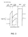
- the data "0" and “1” are stored as potential difference in the channel body, that is, as difference in a threshold voltage of the MISFET. Namely, as shown in Fig. 2, a threshold voltage Vth1 in a data "1" state in which the channel body potential Vbody is high due to hole accumulation is lower than a threshold voltage Vth0 in a data "0" state. In order to maintain the "1" data state in which the holes are accumulated in the channel body, it is preferable that a voltage VWL applied to the word line WL is kept in the negative. This data holding state is not changed even when a read operation is performed as long as the read operation is performed in a linear region and a write operation of inverted data is not performed. Namely, unlike the DRAM in which each memory cell has one transistor and one capacitor and which utilizes charge storage by the capacitor, non-destructive read-out is possible.
- reading data is performed to detect a difference of a conductivity of the memory cell MC. Since the relation between the word line voltage VWL and the channel body potential Vbody is shown in Fig. 2, for example, the word line WL is given a read voltage, which has an intermediate value between the threshold voltages Vth0 and Vth1 of the data "0" and "1", to detect whether or not a current is passed through the memory cell MC, whereby the data can be detected. Or, the word line voltage VWL in excess of the threshold voltages Vth0 and Vth1 is given to the word line WL to detect whether the current of the memory cell MC is large or small, whereby the data can be detected.
- the memory cell MC shown in Fig. 1 has the so-called PD-type MISFET in which the electric neutral region exists in the channel body region.
- PD-type MISFET in which the electric neutral region exists in the channel body region.
- Vfg the voltage for forming the channel
- a depletion layer extends to the intermediate point of the channel body, the electric neutral region remains near the bottom of the channel body.
- an impurity concentration of the channel body also has to increase.
- a leak current in a pn junction increases exponentially with the impurity concentration of the channel body.
- a diffusion current a generation and recombination current and a thermal field emission current (G. Vincent, A. Chantre and D. Bois, "Electric Field Effect on the Thermal Emission of Traps in Semiconductor Junctions," J.Appl.Phys.,50, pp.5484-5487, 1979) in components of the leak current in the pn junction.
- the two formers of them that is, the diffusion current and the generation and recombination current are components which decrease if the impurity concentration NA increases.
- the diffusion current decreases due to a reducibility of a concentration of minority carriers in the electric neutral region if the impurity concentration NA increases, and the generation and recombination current decreases due to a reduction of the depletion layer width if the impurity concentration NA increases.
- the last components is observed as the leak current because electrons in a deep level of the silicon band gap is emitted by thermal energy and then probability of contribution to conduction is increased by strong electric field in the depletion layer. Namely, it is due to a tunnel effect. According to this theory, since the leak current exponentially depends on the strength of the electric field, the leak current exponentially increases depending on the increase of impurity concentration NA.
- a signal amount ⁇ Vth
- which is a difference between the threshold voltage Vth0 in the "0" data cell and the threshold voltage Vth1 in the “1" data cell, is defined by substrate bias effect.
- the substrate bias effect becomes weaker. Therefore, it is necessary that the impurity concentration of the channel body is increased to secure the enough signal amount ⁇ Vth. In conclusion, securing the large signal amount is incompatible with improving characteristics of data holding.
- the memory cell is composed of a full depletion type MISFET so as to suppress the leak current in a scale-down and secure good characteristics of data holding.
- the impurity concentration and the thickness of the channel body is set such that the channel body is fully depleted when a voltage is applied to the gate to form the channel.
- Such a MISFET is referred to as an FD-type MISFET hereinafter.
- Figs. 4A and 4B show a memory cell structure according to a first embodiment using the FD-type MISFET.
- the memory cell MC has an SOI substrate in which an insulating film 12 like a silicon oxide film is formed on a silicon substrate 11 and a p-type silicon layer 13 is formed on the insulating film 11. Since the insulating film 12 is buried under the silicon layer 13, the insulating film 12 is referred to as a BOX (buried oxide) layer hereinafter.
- BOX buried oxide
- the memory cell MC is an n-channel MISFET and it has a main gate 15 formed on the p-type silicon layer 13 via a gate insulating film 14 and source and drain diffusion regions 16 and 17 which are formed with a self-aligned process using the main gate 15 and reach to the bottom of the silicon layer 13.
- the p-type silicon layer 13 has an acceptor concentration NA and a thickness such that it is fully depleted when a gate voltage is applied to the main gate 15 to form a channel in its surface. More specifically, the thickness of the depletion layer extended from the surface of the p-type silicon layer 13 can be expressed as (4 ⁇ Si ⁇ ⁇ F /q ⁇ NA) 1/2 , where the ⁇ f is Fermi-potential and the ⁇ Si is a dielectric constant of silicon.
- condition of the full depletion type MISFET is (4 ⁇ Si ⁇ ⁇ F /q ⁇ NA) 1/2 > tSi.
- the silicon substrate 11 is p-type and an n + -type diffusion layer 18 is formed between the silicon substrate 11 and the BOX layer 12.
- the n + -type diffusion layer 18 is an auxiliary gate to apply a predetermined electric field to the back face of the channel body composed of the p-type silicon layer 13 by capacitive coupling.
- the n + -type diffusion layer 18 is formed as a common gate (back plate) at least throughout the cell array region.
- the case where a negative bias voltage is applied to the channel body from its back face is considered herein, so that the n + -type diffusion layer 18 is formed as the auxiliary gate.
- the n + -type diffusion layer 18 is not formed, but the silicon substrate 11 may be used as the auxiliary gate in itself.
- a p + -type diffusion layer may be formed as the auxiliary gate.
- the memory cells MC are arranged in the form of a matrix so as to isolate each channel body from one another in a width direction in a floating state, too.
- the n + -type diffusion layer 18 being the auxiliary gate is formed throughout the cell array region. In a peripheral region of the cell array region, the n + -type diffusion layer 18 is connected to an auxiliary gate terminal thereabove via a contact plug 20, which is a polysilicon or the like and embedded in the BOX layer 12 and an interlayer insulating film 19 formed on the n + -type diffusion layer 18.
- the BOX layer 12 has the thickness of 30 through 50 nm, and it is relatively thin in order to be easy to apply the electric field to the channel body from its back face.
- Fig. 5 shows a band structure when a surface channel is formed by contrast with Fig. 3.
- Vbg bias voltage
- the channel body is fully depleted by the electric field from the main gate and then the bias voltage Vbg is applied to the channel body by the auxiliary gate to realize the state in which a hole accumulating layer (p-type accumulated layer) is formed in the portion of the back side face of the channel body.
- Fig. 6 shows this state by contrast with Fig. 5.
- the voltage Vfg on the main gate and the voltage Vbg on the auxiliary gate fully deplete the channel body to form the state in which holes can be accumulated in the bottom portion of the channel body, and then this state is regarded as the "0" state of the memory cell.
- this "0" state is moved into a thermal equilibirum state in which holes are accumulated in the bottom portion of the channel body, and then it is defined as the "1" data holding state.
- a forward current is sent between the drain region and the channel body to form a state in which the holes in the channel body are emitted (that is, an non-equilibrium state in which the channel body is fully depleted).
- the impact ionization is generated by a pentode operation to form a state in which the holes are accumulated in the bottom of the channel body.
- the ⁇ FB is a flat band voltage between the main gate 15 formed of the n-type polysilicon and the p-type silicon layer 13 (channel body) in the MOS structure
- the ⁇ F is Fermi-potential
- the ⁇ bs is a potential of the back face of the channel body
- Vbgacc is a value of the auxiliary gate voltage Vbg necessary for accumulating the majority carriers in the portion of the back face of the silicon layer 13, and it is expressed by the following equation (3).
- Vbgacc ⁇ FB -Csi/Cbox ⁇ 2 ⁇ F -Qdep/2Cbox+(1+Csi/Cbox) ⁇ ⁇ bs
- the ⁇ bs is a potential of the back face of the silicon layer 13.
- the ⁇ bs is 0 V.
- This state is a stable state obtained by applying the voltage necessary for fully depleting the silicon layer 13 to the main gate and the voltage Vbgacc to the auxiliary gate. In other words, this is also a state in which the "1" data is written with the pentode region operation of the memory cell and the generation of the majority carriers.
- the potential ⁇ bs of the portion of the back face of the silicon layer 13 is not 0 V but negative value.
- the memory cell structure keeps the stable state (full depletion state) in which the non-equilibrium state cannot exist when the Vbg is larger than -3V whereas the memory cell structure is in unstable state in which the non-equilibrium state can exist when the Vbg is more negative than -3V. It can be said that a system including this non-equilibrium state is used as the DRAM cell in this embodiment. That is, the state to hold the "1" data is the thermal equilibrium state.
- the "0" data state (in which threshold voltage Vth is high) is the non-equilibrium state in which at least a part of the accumulated majority carriers is emitted, and this state is the unstable state which will return to the "1" data if it is held for a long time.
- the ⁇ ⁇ bs is a potential difference in back face of the silicon layer 13 between the "0" data state and the "1" data state.
- the ratio of the Csi to the Cox namely tox/tsi may be larger or the ⁇ ⁇ bs may be larger in order to increase the signal amount.
- the former is condition of the device structure and the latter means signal becomes large if the potential of the bit line is negative enough on the "0" data writing operation.
- the signal amount does not depend on the impurity concentration of the channel body, and it is different from the memory cell using the PD-type MISFET.
- the conditions that the signal amount increases as the Cox is smaller namely the thickness tox of the gate oxide film is thicker is the same.
- the PD-type MISFET has a large short channel effect, so that the tox cannot be thickened.
- the tox can be thickened. Furthermore, viewed in the structure, the fact that the signal amount depends on only tox/tsi means that the signal amount can be kept constant if this ratio remains even though the channel length is more shortened in the future. Hence, it indicates that the scale-down is possible.
- the followings are an actual result of the two-dimensional device simulation for verification of the memory operation.
- Fig. 8 shows a diagram in the case where the "0" read operation subsequent to the "0" write operation is performed
- Fig. 9 shows a diagram in the case where the "1" read operation subsequent to the “1” write operation is performed.
- the gate voltage is raised from -4V to 1V, and next, the drain voltage is lowered from 0V to -1.5V, so that the "0" data write operation is performed. Then, the gate voltage is returned to -4V and the drain voltage is returned to approximately 0V at timing of 2.5E-08. This timing indicates the data holding state and then the read operation is performed with raising the gate voltage again.
- the gate voltage is raised from -4V to 1V, and next, the drain voltage is raised from 0V to 1.5V, so that the "1" data write operation is performed. Then, the gate voltage is returned to -4V and the drain voltage is returned to approximately 0V at timing of 2.5E-08. This timing indicates the data holding state and then the read operation is performed with raising the gate voltage again.
- the source voltage (fixed potential line voltage) is 0V in both cases.
- Fig. 10 is a diagram showing characteristics of the drain current Id versus gate voltage Vgs of the "0" data read operation and "1" data read operation, where Ids0 indicates characteristics of the "0" data read operation and Ids1 indicates characteristics of the "1" data read operation.
- the enough signal amount can be secured because the signal amount ⁇ Vth is approximately 500mV in the data read operations.
- Fig. 11 shows a dependency of the auxiliary gate voltage Vbg concerning the Vth0 in the "0" data and the Vth1 in the "1" data, and this is obtained by the same device simulation with the auxiliary gate voltage Vbg changed. This coincides with Fig. 7 of theoretical calculation.
- Figs. 12A and 12B shows a sectional structure of a memory cell MC according to a second embodiment by contrast with Figs. 4A and 4B.
- a p + -type polysilicon layer 21 is buried under the BOX layer 12 as the auxiliary gate instead of the diffusion layer 18.
- the p + -type polysilicon layer 21 is an impurity doping layer between the semiconductor substrate 11 and the silicon layer 13.
- the p + -type polysilicon layer 21 may be formed as a common electrode at least throughout the cell array region.
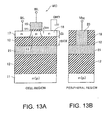
- Figs. 13A and 13B show a memory cell structure according to a third embodiment by contrast with Figs. 12A and 12B.
- the BOX layer 12 is thicker, and the polysilicon layer (impurity doping layer) 21 is buried in the BOX layer 12 as the auxiliary gate.
- the p + -type polysilicon layer 21 may be formed as a common electrode at least throughout the cell array region.
- Figs. 14A and 14B shows a memory cell structure according to a fourth embodiment in which the structure of Figs. 13A and 13B is slightly modified.
- the polysilicon layer 21 buried in the BOX layer 12 is formed as a plate line (auxiliary word line) in the stripe form in parallel with the word line WL composed of the gate electrode 15.
- the polysilicon layer 21 is connected to a supply terminal of the auxiliary gate voltage Vbg via the contact plug at the end portion of the word line direction, for example, at the end portion opposite to the side where a word line driver is arranged.
- Figs. 14A and 14B in which the auxiliary gates are separated from one another can be also applied to the diffusion layer 18 in Figs. 4A and 4B of the first embodiment, the polysilicon layer 21 in Figs. 12A and 12B and Figs. 13A and 13B of the second and third embodiments.
- a lateral transistor in which the channel is formed in parallel with the substrate face is used as the MISFET
- a vertical transistor in which the channel is formed perpendicular to the substrate face may be used.
- a sectional structure of a portion of two memory cells in such a manner is shown in Fig. 15.
- An n-type layer 32 is formed on an entire surface of a p-type silicon substrate 31, pillar shaped p-type silicon portions 33 are patterned and formed in each memory cell region on the n-type silicon layer 32.
- the p-type silicon layer 32 is a common source for all the memory cells.
- a main gate 36 is formed via a gate insulating film 35 on the one vertical side of the silicon portion 33 whereas an auxiliary gate 38 is formed via a gate insulating film 37 on the other vertical side thereof.
- the main gate 36 and the auxiliary gate 38 are continuously formed in one direction in parallel as a word line WL and a plate line PL, respectively.
- a drain diffusion region 34 is formed in the top portion of each p-type silicon portion 33.
- a bit line 41 connected to each drain region 34 is provided on an interlayer insulating film 40.
- the thickness of the p-type silicon portion 33 (width of lateral direction in this drawing) and the impurity concentration is chosen so as to be the FD-type MISFET, thereby the same operation as the above-mentioned embodiments can be realized.
- Figs. 16A and 16B also show sectional views of a vertical MISFET, however, the auxiliary gate for controlling the potential of the portion of the back side face of the channel body is not directly opposite to the back side face thereof, but a pair of auxiliary gates are opposite to each other at the bottom portion of the both side faces.
- the n + -type diffusion layer 18 is formed under the BOX layer 12, but the BOX layer 12 is thicker. Therefore, as shown in Fig. 16B showing the sectional view taken along the word line WL, polysilicon portions 22 are buried in the BOX layer 12 so as to be opposite to each other via gate insulating films 23 in the bottom portion of the p-type silicon layer 13.
- the polysilicon portions 22 are buried on both sides of the p-type silicon layer 13, and the bottom of the polysilicon portions 22 are connected to the n + -type diffusion layer 18.
- the polysilicon portions 22 are auxiliary gates for controlling a potential of the bottom portion of the p-type silicon layer 13 with capacitive coupling.
- the gate length L and gate width W are 0.175 ⁇ m
- the gate oxide film thickness toxf of the main gate 15 side is 6.5 nm
- the acceptor concentration NA of the channel body is 1.0 ⁇ 10 15 cm -3
- both the main gate 15 and the auxiliary gate 22 are the n + -type polysilicon
- the auxiliary gate voltage Vbg is -4V
- the gate oxide film thickness toxb of the auxiliary gate side is 15nm
- the thickness tSi of the silicon layer 13 is 140nm
- the BOX layer thickness is 200nm.
- the polysilicon portions 22 are buried up to the middle height of the channel body.
- Figs. 17 and 18 show operating waveforms of the "0" data write/read and the "1" data write/read and correspond to Figs. 8 and 9 in the first embodiment, respectively.
- n-channel MISFET having the channel body of p-type silicon is used.
- a MISFET having the channel body of an intrinsic silicon which does not substantially include impurity. That way, there is no leak current caused by crystalline unconformity in the channel body because of impurity diffusion and so on, so that data holding characteristics are improved further.
- Vth of the MISFET is positive, it is necessary to use p + -type polysilicon for the main gate. However, even if the threshold voltage is negative, it is enough that the operation is performed in the condition that the word line level is lowered by approximately 1V, so that an n + -type polysilicon may be used for the main gate.
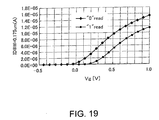
- Fig. 20A shows a calculation result of a relation of the threshold voltages Vth0 and Vth1 in the "0" data and "1" data versus the auxiliary gate voltage Vbg in the case where the intrinsic silicon is used as the channel body in the MISFET, by contrast with the Fig. 11.
- the assumption is made that the p + -type polysilicon is used for the main gate.
- the back face potential of the channel body in the "0" data cell is not lowered by a large amount in a negative direction but the channel body is in the full depletion state in which the majority carriers are not accumulated.
- the auxiliary gate voltage Vbg may be set between the value at which the majority carriers are accumulated in the channel body in the "1" data cell and the value at which the majority carriers are accumulated in the channel body in the "0" data cell. In accordance with the result of Fig. 20A in this embodiment, it is set in the range of -2.0V ⁇ Vbg ⁇ 0.5V. However, if the data holding time is set longer than required specification, it is preferable that the voltage Vbg is set at the value smaller than the value capable of accumulating the majority carriers in the channel body in the "0" data cell and then the signal amount is maximized.
- Table 1 shows characteristic changes owing to fluctuation of various device parameters when the DRAM according to the above-mentioned embodiment is manufactured.
- Table 1 sample No. 0 1 2 3 4 5 6 NA[cm -3 ] 1E+15 1E+15 1E+15 1E+15 1E+15 1E+15 tox[nm] 10 10 10 10 10 8 12 tBOX[nm] 30 30 30 20 40 30 30 tSi[nm] 25 15 35 25 25 25 25 25 25 25 25 25 25 25 25 25 25 25 25 25 25 25 25 25 25 25 Vbg0[V] -5 -7.5 -4 -4 -6.5 -5 -5 Vbg1[V] -3 -4.5 -2.25 -2 -3.5 -3 Vbgs[V] -4.5 -6.75 -3.56 -3.5 -5.75 -4.5 -4.5 Vth0[mV] 1050 1800 710 1100 1050 810 1290 Vth1[mV] 620 1100 410 610 610
- the Vbg0 indicates the maximum auxiliary gate voltage necessary for accumulating the majority carriers (holes) in the channel body in the "0" data cell
- the Vbg1 indicates the maximum auxiliary gate voltage necessary for accumulating the majority carriers (holes) in the channel body in the "1" data cell.
- Vbgs Vbg0+(Vbg1-Vbg0) ⁇ 0.25, under the condition that the channel body is fully depleted on the "0" data holding on the basis of conditions for acquiring large signal amount.
- Table 1 further shows the threshold voltage Vth0 of the "0" data cell, the threshold voltage Vth1 of the "1" data cell and the difference ⁇ Vth therebetween then.
- the optimum setting voltage Vbgs of the auxiliary gate is changed in the range of -3.5V through -6.75V.
- the threshold voltage Vth0 of the "0" data cell is changed in the range of 710mV through 1800mV whereas the threshold voltage Vth1 of the "1" data cell is changed in the range of 410mV through 1100mV
- auxiliary gate voltage Vbgs There are various method for the adjusting of the auxiliary gate voltage Vbgs and the above-mentioned word line potential VWLHW/VWLHR/VWLL.
- a test MISFET having the same structure as the memory cell is provided for each chip.
- the chip selecting test is performed, the "0" data write/read operation and the "1" data write/read operation are performed to/from the test MISFET, and then the threshold voltages Vth0 and Vth1 are measured in a triode region of the test MISFET.
- the same tests are repeated with the auxiliary gate voltage Vbg changed, and the optimum auxiliary gate voltage Vbg is decided.
- Fig. 20B is a diagram showing such a chip structure.
- the chip has a mimic transistor 90 in addition to a memory cell array 80.
- the mimic transistor 90 has the same structure as the memory cells MC in the memory cell array 80. However, there are difference points that its main gate MG, source region S, drain region D and auxiliary gate AG are connected to pads 92, 94, 96 and 98, respectively. That is, the chip has the pads 92, 94, 96 and 98 to test the mimic transistor 90.
- the main gate voltage Vfg can be directly applied to the main gate MG from the pad 92, and the auxiliary gate voltage Vbg can be directly applied to the auxiliary gate AG from the pad 98. Moreover, by measuring a current flowing between the pad 94 and the pad 96, a current flowing between the source region S and the drain region D of the mimic transistor 90 can be directly measured. As a result, it is possible to write the "1" data into the mimic transistor 90 and the "0" data into the mimic transistor 90. Furthermore, it is possible to easily measure the threshold voltage Vth1 of the "1" data write state and the threshold voltage Vth0 of the "0" data write state.
- the chip Since the chip has the mimic transistor 90 of this structure, it is possible to accurately measure what voltage the auxiliary gate Vbg, what voltage the high level voltage VWLHW of the word line on the write operation, the voltage VWLHR of the word line on the read operation and the low level voltage VWLL of word line on the holding state should be adjusted.
- a nonvolatile memory circuit like fuses is mounted on the memory chip as an initial setting data memory circuit to initially set operation conditions. Then, in accordance with the result of the above-mentioned test, the fuses are programmed. The programmed data are read when power is turned on, an auxiliary gate voltage setting circuit, a word line voltage generating circuit and so on for VWLHW/VWLHR/VWLL are initially set. In this manner, it is possible to set the optimum operation condition for each memory chip.
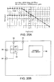
- Fig. 21 shows a layout of a concrete cell array according to the first embodiment
- Figs. 22, 23 and 24 are sectional diagrams taken along the lines I-I', II-II' and III-III' in Fig. 21, respectively.
- the p-type silicon layers 13 of the SOI substrate are defined as element forming regions in the form of stripes extending in the bit line direction by an element isolation insulating film 106, which is the STI (shallow trench isolation).
- the MISFETs are formed and arranged such that the source region 16 and the drain region 17 in the each p-type silicon layer 13 are shared between neighboring MISFETs in the bit line direction, respectively.
- the gate electrodes 15 are continuously formed as word lines WL in the direction intersecting the bit lines BL, specifically, perpendicular to the bit lines BL.
- the top face and both side faces are covered with silicon nitride film 101.
- common source lines 102 SL
- bit lines 105 BL are formed on the interlayer insulating film 103, and each bit line 105 is connected to drain regions 17 of the MISFETs.
- the n + -type layer 18 as the auxiliary gate is formed as a common electrode throughout the whole cell array.
- a unit cell area is 4F 2 indicated by one dotted chain line in Fig. 21.
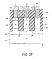
- Fig. 25 shows a layout of a concrete cell array according to the fifth embodiment in which the basic cell structure is shown in Fig. 15, and Figs. 26 and 27 are sectional diagrams taken along the lines I-I' and II-II' in Fig. 25, respectively.
- a silicon wafer having p/n/p structure is used, and grooves whose depth reach the n-type layer 32 are formed, so that pillar type and p-type silicon portions 33 are formed and arranged.
- the insulating film 39 is buried in the grooves.
- main gates 36 and the auxiliary gates 38 are buried at both sides of each silicon portion 33 such that the main gates 36 are opposite to the auxiliary gates 38 via the gate insulating films 35 and 37.
- the main gates 36 and the auxiliary gates 38 are formed and patterned as word lines WL and plate lines (auxiliary word lines) PL in parallel with one another.
- the gate insulating films 35 and 37 are formed with the same process when the thickness of the gate insulating films 35 and 37 are the same, separate processes are needed when they have different thickness.
- the top face and the both side faces of the main gates 36 and the auxiliary gates 38 are covered with silicon nitride films 110.
- the interlayer insulating film 40 is deposited. Contact plugs 112 are buried in the interlayer insulating film 40, the bit lines 41 (BL) are provided on the interlayer insulating film 40, and then the cell array is constituted.
- each plate line PL is arranged between two word lines WL and WL so as to be shared between two neighboring memory cells in the bit line direction.
- a unit cell area is 6F 2 .
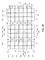
- Fig. 28 shows a layout of a concrete cell array according to the sixth embodiment in which the basic cell structure is shown in Fig. 16, and Figs. 29, 30 and 31 are sectional diagrams taken along the lines I-I', II-II' and III-III' in Fig. 28, respectively.
- the basic cell array structure of Figs. 28 and 29 is the same as that of Figs. 21 and 22.
- the polysilicon portions 22 are buried to constitute auxiliary gates in parallel with the bit lines BL at each position between bit lines BL and BL.
- the polysilicon portions 22 are buried in the BOX layer 12 so as to be opposite to each other at the bottom side faces of each p-type silicon portion 13. In this embodiment, their top faces are located at the middle of thickness of the p-type silicon portions 13, so that they constitute the plate lines (auxiliary word lines) PL.
- the word lines WL are the main gates in the memory cell array 201, and they are selectively driven by a row decoder (including a word line driver) 205.
- the bit lines BL are connected to a sense amplifier 202, and then the data write and the data read is performed between the bit lines of the column selected by a column decoder 203 and an I/O terminal via a data buffer 204.
- An address signal is input to an address buffer 206, a row address is decoded by the row decoder 205 and a column address is decoded by the column decoder 203.
- Various control signals applied to the word lines in the cell array 201 via the row decoder 205 and the auxiliary gate voltage Vbg applied to the auxiliary gate are generated by an internal voltage generating circuit 207 using a booster circuit and so on.
- the various control signals include a high level voltage VWLHW of the word line on the write operation, a voltage VWLHR of the word line on the read operation and a low level voltage VWLL of word line on the holding state.
- An initial setting resistor 209 is provided in order to set an output voltage from the internal voltage generating circuit 207 at the optimum value in each chip.
- a fuse circuit 208 is provided as the nonvolatile memory circuit in order to set various voltages output from the internal voltage generating circuit 207 at the optimum value.
- initial setting values of the various voltages are decided.
- a power-on detecting circuit 210 detects a power-on and the data in the fuse circuit 208 is automatically read into the initial setting resistor 209 based on the output from the power-on detecting circuit 210.
- the internal voltage generating circuit 207 is controlled by the output from the initial setting resistor 209, so that the optimum control voltage VWL, the auxiliary gate voltage Vbg and so on are generated in each chip.
Landscapes
- Semiconductor Memories (AREA)
- Dram (AREA)
- Thin Film Transistor (AREA)
- Non-Volatile Memory (AREA)
Applications Claiming Priority (2)
| Application Number | Priority Date | Filing Date | Title |
|---|---|---|---|
| JP2001220461A JP2003031693A (ja) | 2001-07-19 | 2001-07-19 | 半導体メモリ装置 |
| JP2001220461 | 2001-07-19 |
Publications (2)
| Publication Number | Publication Date |
|---|---|
| EP1280205A2 true EP1280205A2 (de) | 2003-01-29 |
| EP1280205A3 EP1280205A3 (de) | 2009-10-07 |
Family
ID=19054277
Family Applications (1)
| Application Number | Title | Priority Date | Filing Date |
|---|---|---|---|
| EP01123208A Withdrawn EP1280205A3 (de) | 2001-07-19 | 2001-10-01 | Halbleiter-Speicherbauteil |
Country Status (6)
| Country | Link |
|---|---|
| US (2) | US6617651B2 (de) |
| EP (1) | EP1280205A3 (de) |
| JP (1) | JP2003031693A (de) |
| KR (1) | KR100440188B1 (de) |
| CN (1) | CN1217415C (de) |
| TW (1) | TW519751B (de) |
Cited By (61)
| Publication number | Priority date | Publication date | Assignee | Title |
|---|---|---|---|---|
| EP1494287A1 (de) * | 2003-07-01 | 2005-01-05 | STMicroelectronics S.A. | DRAM-Bauteil mit zwei Speicherzellen und Verfahrung zu seiner Herstellung |
| US6873539B1 (en) | 2001-06-18 | 2005-03-29 | Pierre Fazan | Semiconductor device |
| US6912150B2 (en) | 2003-05-13 | 2005-06-28 | Lionel Portman | Reference current generator, and method of programming, adjusting and/or operating same |
| EP1494288A3 (de) * | 2003-06-30 | 2005-12-14 | Kabushiki Kaisha Toshiba | Halbleiterspeicherelement und integrierter Halbleiterschaltkreis |
| US6982918B2 (en) | 2002-04-18 | 2006-01-03 | Pierre Fazan | Data storage device and refreshing method for use with such device |
| US7061050B2 (en) | 2002-04-18 | 2006-06-13 | Innovative Silicon S.A. | Semiconductor device utilizing both fully and partially depleted devices |
| US7085156B2 (en) | 2003-05-13 | 2006-08-01 | Innovative Silicon S.A. | Semiconductor memory device and method of operating same |
| US7085153B2 (en) | 2003-05-13 | 2006-08-01 | Innovative Silicon S.A. | Semiconductor memory cell, array, architecture and device, and method of operating same |
| US7177175B2 (en) | 2003-09-24 | 2007-02-13 | Innovative Silicon S.A. | Low power programming technique for a floating body memory transistor, memory cell, and memory array |
| US7251164B2 (en) | 2004-11-10 | 2007-07-31 | Innovative Silicon S.A. | Circuitry for and method of improving statistical distribution of integrated circuits |
| US7301838B2 (en) | 2004-12-13 | 2007-11-27 | Innovative Silicon S.A. | Sense amplifier circuitry and architecture to write data into and/or read from memory cells |
| US7301803B2 (en) | 2004-12-22 | 2007-11-27 | Innovative Silicon S.A. | Bipolar reading technique for a memory cell having an electrically floating body transistor |
| US7335934B2 (en) | 2003-07-22 | 2008-02-26 | Innovative Silicon S.A. | Integrated circuit device, and method of fabricating same |
| US7355916B2 (en) | 2005-09-19 | 2008-04-08 | Innovative Silicon S.A. | Method and circuitry to generate a reference current for reading a memory cell, and device implementing same |
| US7476939B2 (en) | 2004-11-04 | 2009-01-13 | Innovative Silicon Isi Sa | Memory cell having an electrically floating body transistor and programming technique therefor |
| US7492632B2 (en) | 2006-04-07 | 2009-02-17 | Innovative Silicon Isi Sa | Memory array having a programmable word length, and method of operating same |
| US7542340B2 (en) | 2006-07-11 | 2009-06-02 | Innovative Silicon Isi Sa | Integrated circuit including memory array having a segmented bit line architecture and method of controlling and/or operating same |
| US7542345B2 (en) | 2006-02-16 | 2009-06-02 | Innovative Silicon Isi Sa | Multi-bit memory cell having electrically floating body transistor, and method of programming and reading same |
| US7606066B2 (en) | 2005-09-07 | 2009-10-20 | Innovative Silicon Isi Sa | Memory cell and memory cell array having an electrically floating body transistor, and methods of operating same |
| US7606098B2 (en) | 2006-04-18 | 2009-10-20 | Innovative Silicon Isi Sa | Semiconductor memory array architecture with grouped memory cells, and method of controlling same |
| US7683430B2 (en) | 2005-12-19 | 2010-03-23 | Innovative Silicon Isi Sa | Electrically floating body memory cell and array, and method of operating or controlling same |
| US7924630B2 (en) | 2008-10-15 | 2011-04-12 | Micron Technology, Inc. | Techniques for simultaneously driving a plurality of source lines |
| US7933142B2 (en) | 2006-05-02 | 2011-04-26 | Micron Technology, Inc. | Semiconductor memory cell and array using punch-through to program and read same |
| US7933140B2 (en) | 2008-10-02 | 2011-04-26 | Micron Technology, Inc. | Techniques for reducing a voltage swing |
| US7947543B2 (en) | 2008-09-25 | 2011-05-24 | Micron Technology, Inc. | Recessed gate silicon-on-insulator floating body device with self-aligned lateral isolation |
| US7957206B2 (en) | 2008-04-04 | 2011-06-07 | Micron Technology, Inc. | Read circuitry for an integrated circuit having memory cells and/or a memory cell array, and method of operating same |
| US8014195B2 (en) | 2008-02-06 | 2011-09-06 | Micron Technology, Inc. | Single transistor memory cell |
| US8064274B2 (en) | 2007-05-30 | 2011-11-22 | Micron Technology, Inc. | Integrated circuit having voltage generation circuitry for memory cell array, and method of operating and/or controlling same |
| US8069377B2 (en) | 2006-06-26 | 2011-11-29 | Micron Technology, Inc. | Integrated circuit having memory array including ECC and column redundancy and method of operating the same |
| US8085594B2 (en) | 2007-06-01 | 2011-12-27 | Micron Technology, Inc. | Reading technique for memory cell with electrically floating body transistor |
| US8139418B2 (en) | 2009-04-27 | 2012-03-20 | Micron Technology, Inc. | Techniques for controlling a direct injection semiconductor memory device |
| US8174881B2 (en) | 2009-11-24 | 2012-05-08 | Micron Technology, Inc. | Techniques for reducing disturbance in a semiconductor device |
| US8189376B2 (en) | 2008-02-08 | 2012-05-29 | Micron Technology, Inc. | Integrated circuit having memory cells including gate material having high work function, and method of manufacturing same |
| US8194487B2 (en) | 2007-09-17 | 2012-06-05 | Micron Technology, Inc. | Refreshing data of memory cells with electrically floating body transistors |
| US8199595B2 (en) | 2009-09-04 | 2012-06-12 | Micron Technology, Inc. | Techniques for sensing a semiconductor memory device |
| US8213226B2 (en) | 2008-12-05 | 2012-07-03 | Micron Technology, Inc. | Vertical transistor memory cell and array |
| US8223574B2 (en) | 2008-11-05 | 2012-07-17 | Micron Technology, Inc. | Techniques for block refreshing a semiconductor memory device |
| US8264041B2 (en) | 2007-01-26 | 2012-09-11 | Micron Technology, Inc. | Semiconductor device with electrically floating body |
| US8310893B2 (en) | 2009-12-16 | 2012-11-13 | Micron Technology, Inc. | Techniques for reducing impact of array disturbs in a semiconductor memory device |
| US8315099B2 (en) | 2009-07-27 | 2012-11-20 | Micron Technology, Inc. | Techniques for providing a direct injection semiconductor memory device |
| US8319294B2 (en) | 2009-02-18 | 2012-11-27 | Micron Technology, Inc. | Techniques for providing a source line plane |
| US8349662B2 (en) | 2007-12-11 | 2013-01-08 | Micron Technology, Inc. | Integrated circuit having memory cell array, and method of manufacturing same |
| US8369177B2 (en) | 2010-03-05 | 2013-02-05 | Micron Technology, Inc. | Techniques for reading from and/or writing to a semiconductor memory device |
| US8411513B2 (en) | 2010-03-04 | 2013-04-02 | Micron Technology, Inc. | Techniques for providing a semiconductor memory device having hierarchical bit lines |
| US8411524B2 (en) | 2010-05-06 | 2013-04-02 | Micron Technology, Inc. | Techniques for refreshing a semiconductor memory device |
| US8416636B2 (en) | 2010-02-12 | 2013-04-09 | Micron Technology, Inc. | Techniques for controlling a semiconductor memory device |
| US8498157B2 (en) | 2009-05-22 | 2013-07-30 | Micron Technology, Inc. | Techniques for providing a direct injection semiconductor memory device |
| US8508994B2 (en) | 2009-04-30 | 2013-08-13 | Micron Technology, Inc. | Semiconductor device with floating gate and electrically floating body |
| US8518774B2 (en) | 2007-03-29 | 2013-08-27 | Micron Technology, Inc. | Manufacturing process for zero-capacitor random access memory circuits |
| US8531878B2 (en) | 2011-05-17 | 2013-09-10 | Micron Technology, Inc. | Techniques for providing a semiconductor memory device |
| US8537610B2 (en) | 2009-07-10 | 2013-09-17 | Micron Technology, Inc. | Techniques for providing a semiconductor memory device |
| US8536628B2 (en) | 2007-11-29 | 2013-09-17 | Micron Technology, Inc. | Integrated circuit having memory cell array including barriers, and method of manufacturing same |
| US8547738B2 (en) | 2010-03-15 | 2013-10-01 | Micron Technology, Inc. | Techniques for providing a semiconductor memory device |
| US8576631B2 (en) | 2010-03-04 | 2013-11-05 | Micron Technology, Inc. | Techniques for sensing a semiconductor memory device |
| US8710566B2 (en) | 2009-03-04 | 2014-04-29 | Micron Technology, Inc. | Techniques for forming a contact to a buried diffusion layer in a semiconductor memory device |
| US8748959B2 (en) | 2009-03-31 | 2014-06-10 | Micron Technology, Inc. | Semiconductor memory device |
| US8773933B2 (en) | 2012-03-16 | 2014-07-08 | Micron Technology, Inc. | Techniques for accessing memory cells |
| US9559216B2 (en) | 2011-06-06 | 2017-01-31 | Micron Technology, Inc. | Semiconductor memory device and method for biasing same |
| WO2023279420A1 (zh) * | 2021-07-05 | 2023-01-12 | 长鑫存储技术有限公司 | 存储器及其制造方法 |
| US11985808B2 (en) | 2021-07-05 | 2024-05-14 | Changxin Memory Technologies, Inc. | Memory and method for manufacturing same |
| US12108588B2 (en) | 2021-07-05 | 2024-10-01 | Changxin Memory Technologies, Inc. | Memory and method for manufacturing same |
Families Citing this family (85)
| Publication number | Priority date | Publication date | Assignee | Title |
|---|---|---|---|---|
| US6642133B2 (en) * | 2001-12-20 | 2003-11-04 | Intel Corporation | Silicon-on-insulator structure and method of reducing backside drain-induced barrier lowering |
| JP2003309182A (ja) * | 2002-04-17 | 2003-10-31 | Hitachi Ltd | 半導体装置の製造方法及び半導体装置 |
| US6865407B2 (en) * | 2002-07-11 | 2005-03-08 | Optical Sensors, Inc. | Calibration technique for non-invasive medical devices |
| US6888200B2 (en) * | 2002-08-30 | 2005-05-03 | Micron Technology Inc. | One transistor SOI non-volatile random access memory cell |
| US6917078B2 (en) * | 2002-08-30 | 2005-07-12 | Micron Technology Inc. | One transistor SOI non-volatile random access memory cell |
| US7042027B2 (en) * | 2002-08-30 | 2006-05-09 | Micron Technology, Inc. | Gated lateral thyristor-based random access memory cell (GLTRAM) |
| US7710771B2 (en) * | 2002-11-20 | 2010-05-04 | The Regents Of The University Of California | Method and apparatus for capacitorless double-gate storage |
| JP4850387B2 (ja) * | 2002-12-09 | 2012-01-11 | ルネサスエレクトロニクス株式会社 | 半導体装置 |
| JP2004297048A (ja) * | 2003-03-11 | 2004-10-21 | Semiconductor Energy Lab Co Ltd | 集積回路、該集積回路を有する半導体表示装置及び集積回路の駆動方法 |
| US7541614B2 (en) * | 2003-03-11 | 2009-06-02 | Semiconductor Energy Laboratory Co., Ltd. | Integrated circuit, semiconductor device comprising the same, electronic device having the same, and driving method of the same |
| US8125003B2 (en) * | 2003-07-02 | 2012-02-28 | Micron Technology, Inc. | High-performance one-transistor memory cell |
| US7119393B1 (en) * | 2003-07-28 | 2006-10-10 | Actel Corporation | Transistor having fully-depleted junctions to reduce capacitance and increase radiation immunity in an integrated circuit |
| JP4077381B2 (ja) | 2003-08-29 | 2008-04-16 | 株式会社東芝 | 半導体集積回路装置 |
| US7191380B2 (en) * | 2003-09-10 | 2007-03-13 | Hewlett-Packard Development Company, L.P. | Defect-tolerant and fault-tolerant circuit interconnections |
| JP4443886B2 (ja) * | 2003-09-30 | 2010-03-31 | 株式会社東芝 | 半導体記憶装置 |
| JP4044510B2 (ja) | 2003-10-30 | 2008-02-06 | 株式会社東芝 | 半導体集積回路装置 |
| JP4058403B2 (ja) | 2003-11-21 | 2008-03-12 | 株式会社東芝 | 半導体装置 |
| US7002842B2 (en) * | 2003-11-26 | 2006-02-21 | Intel Corporation | Floating-body dynamic random access memory with purge line |
| JP4559728B2 (ja) | 2003-12-26 | 2010-10-13 | 株式会社東芝 | 半導体記憶装置 |
| JP4342970B2 (ja) | 2004-02-02 | 2009-10-14 | 株式会社東芝 | 半導体メモリ装置及びその製造方法 |
| JP4028499B2 (ja) * | 2004-03-01 | 2007-12-26 | 株式会社東芝 | 半導体記憶装置 |
| JP4002900B2 (ja) | 2004-03-02 | 2007-11-07 | 東芝マイクロエレクトロニクス株式会社 | 半導体記憶装置 |
| JP4110115B2 (ja) * | 2004-04-15 | 2008-07-02 | 株式会社東芝 | 半導体記憶装置 |
| JP3962729B2 (ja) | 2004-06-03 | 2007-08-22 | 株式会社東芝 | 半導体装置 |
| US7518182B2 (en) | 2004-07-20 | 2009-04-14 | Micron Technology, Inc. | DRAM layout with vertical FETs and method of formation |
| US7145186B2 (en) | 2004-08-24 | 2006-12-05 | Micron Technology, Inc. | Memory cell with trenched gated thyristor |
| US7158410B2 (en) * | 2004-08-27 | 2007-01-02 | Micron Technology, Inc. | Integrated DRAM-NVRAM multi-level memory |
| US7271433B1 (en) | 2004-09-02 | 2007-09-18 | Micron Technology, Inc. | High-density single transistor vertical memory gain cell |
| US7285812B2 (en) * | 2004-09-02 | 2007-10-23 | Micron Technology, Inc. | Vertical transistors |
| US7259415B1 (en) | 2004-09-02 | 2007-08-21 | Micron Technology, Inc. | Long retention time single transistor vertical memory gain cell |
| US7271052B1 (en) | 2004-09-02 | 2007-09-18 | Micron Technology, Inc. | Long retention time single transistor vertical memory gain cell |
| JP2006073939A (ja) * | 2004-09-06 | 2006-03-16 | Toshiba Corp | 不揮発性半導体記憶装置及び不揮発性半導体記憶装置の製造方法 |
| JP4083160B2 (ja) * | 2004-10-04 | 2008-04-30 | 株式会社東芝 | 半導体記憶装置およびfbcメモリセルの駆動方法 |
| JP4081071B2 (ja) * | 2004-11-26 | 2008-04-23 | 株式会社東芝 | 半導体記憶装置とその製造方法 |
| US7199419B2 (en) * | 2004-12-13 | 2007-04-03 | Micron Technology, Inc. | Memory structure for reduced floating body effect |
| JP4470171B2 (ja) * | 2004-12-15 | 2010-06-02 | エルピーダメモリ株式会社 | 半導体チップ、その製造方法およびその用途 |
| JP4895823B2 (ja) * | 2004-12-28 | 2012-03-14 | スパンション エルエルシー | 半導体装置 |
| JP2006269535A (ja) * | 2005-03-22 | 2006-10-05 | Toshiba Corp | 半導体記憶装置および半導体記憶装置の製造方法 |
| KR100663359B1 (ko) | 2005-03-31 | 2007-01-02 | 삼성전자주식회사 | 리세스 채널 트랜지스터 구조를 갖는 단일 트랜지스터플로팅 바디 디램 셀 및 그 제조방법 |
| US7371627B1 (en) | 2005-05-13 | 2008-05-13 | Micron Technology, Inc. | Memory array with ultra-thin etched pillar surround gate access transistors and buried data/bit lines |
| US7120046B1 (en) | 2005-05-13 | 2006-10-10 | Micron Technology, Inc. | Memory array with surrounding gate access transistors and capacitors with global and staggered local bit lines |
| US7538389B2 (en) * | 2005-06-08 | 2009-05-26 | Micron Technology, Inc. | Capacitorless DRAM on bulk silicon |
| US7517741B2 (en) * | 2005-06-30 | 2009-04-14 | Freescale Semiconductor, Inc. | Single transistor memory cell with reduced recombination rates |
| US7238555B2 (en) * | 2005-06-30 | 2007-07-03 | Freescale Semiconductor, Inc. | Single transistor memory cell with reduced programming voltages |
| JP2007018588A (ja) * | 2005-07-06 | 2007-01-25 | Toshiba Corp | 半導体記憶装置および半導体記憶装置の駆動方法 |
| US7888721B2 (en) | 2005-07-06 | 2011-02-15 | Micron Technology, Inc. | Surround gate access transistors with grown ultra-thin bodies |
| US7768051B2 (en) | 2005-07-25 | 2010-08-03 | Micron Technology, Inc. | DRAM including a vertical surround gate transistor |
| US20070023833A1 (en) * | 2005-07-28 | 2007-02-01 | Serguei Okhonin | Method for reading a memory cell having an electrically floating body transistor, and memory cell and array implementing same |
| US7696567B2 (en) | 2005-08-31 | 2010-04-13 | Micron Technology, Inc | Semiconductor memory device |
| JP4664777B2 (ja) * | 2005-09-07 | 2011-04-06 | 株式会社東芝 | 半導体装置 |
| US20070085140A1 (en) * | 2005-10-19 | 2007-04-19 | Cedric Bassin | One transistor memory cell having strained electrically floating body region, and method of operating same |
| JP2007189017A (ja) * | 2006-01-12 | 2007-07-26 | Toshiba Corp | 半導体装置 |
| JP2007194259A (ja) * | 2006-01-17 | 2007-08-02 | Toshiba Corp | 半導体装置及びその製造方法 |
| JP4373986B2 (ja) * | 2006-02-16 | 2009-11-25 | 株式会社東芝 | 半導体記憶装置 |
| JP2007242950A (ja) * | 2006-03-09 | 2007-09-20 | Toshiba Corp | 半導体記憶装置 |
| US8501581B2 (en) * | 2006-03-29 | 2013-08-06 | Micron Technology, Inc. | Methods of forming semiconductor constructions |
| US7608898B2 (en) * | 2006-10-31 | 2009-10-27 | Freescale Semiconductor, Inc. | One transistor DRAM cell structure |
| JP2008117489A (ja) * | 2006-11-07 | 2008-05-22 | Toshiba Corp | 半導体記憶装置 |
| JP2008124302A (ja) * | 2006-11-14 | 2008-05-29 | Toshiba Corp | 半導体記憶装置およびその製造方法 |
| US8217435B2 (en) | 2006-12-22 | 2012-07-10 | Intel Corporation | Floating body memory cell having gates favoring different conductivity type regions |
| JP2008177273A (ja) * | 2007-01-17 | 2008-07-31 | Toshiba Corp | 半導体記憶装置及び半導体記憶装置の製造方法 |
| JP5019436B2 (ja) * | 2007-02-22 | 2012-09-05 | ルネサスエレクトロニクス株式会社 | 半導体集積回路 |
| US7923373B2 (en) | 2007-06-04 | 2011-04-12 | Micron Technology, Inc. | Pitch multiplication using self-assembling materials |
| JP5130571B2 (ja) * | 2007-06-19 | 2013-01-30 | ルネサスエレクトロニクス株式会社 | 半導体装置 |
| KR100881825B1 (ko) * | 2007-07-27 | 2009-02-03 | 주식회사 하이닉스반도체 | 반도체 소자 및 그 제조 방법 |
| JP2009093708A (ja) * | 2007-10-04 | 2009-04-30 | Toshiba Corp | 半導体記憶装置およびその駆動方法 |
| WO2009087125A1 (en) * | 2008-01-04 | 2009-07-16 | Centre National De La Recherche Scientifique | Double-gate floating-body memory device |
| CN101494222B (zh) | 2008-01-23 | 2010-08-25 | 苏州东微半导体有限公司 | 半导体存储器器件、半导体存储器阵列及写入方法 |
| JP5121475B2 (ja) * | 2008-01-28 | 2013-01-16 | 株式会社東芝 | 半導体記憶装置 |
| KR101505494B1 (ko) | 2008-04-30 | 2015-03-24 | 한양대학교 산학협력단 | 무 커패시터 메모리 소자 |
| JP4751432B2 (ja) * | 2008-09-26 | 2011-08-17 | シャープ株式会社 | 半導体記憶装置 |
| KR20100062212A (ko) * | 2008-12-01 | 2010-06-10 | 삼성전자주식회사 | 반도체 메모리 장치 |
| JP2010157580A (ja) * | 2008-12-26 | 2010-07-15 | Toshiba Corp | 半導体記憶装置 |
| US8148780B2 (en) * | 2009-03-24 | 2012-04-03 | Micron Technology, Inc. | Devices and systems relating to a memory cell having a floating body |
| US7929343B2 (en) * | 2009-04-07 | 2011-04-19 | Micron Technology, Inc. | Methods, devices, and systems relating to memory cells having a floating body |
| US8138541B2 (en) * | 2009-07-02 | 2012-03-20 | Micron Technology, Inc. | Memory cells |
| JP5564918B2 (ja) * | 2009-12-03 | 2014-08-06 | ソニー株式会社 | 撮像素子およびカメラシステム |
| US8421156B2 (en) * | 2010-06-25 | 2013-04-16 | International Business Machines Corporation | FET with self-aligned back gate |
| KR101027702B1 (ko) * | 2010-10-04 | 2011-04-12 | 주식회사 하이닉스반도체 | 플로팅 바디 캐패시터를 구비한 반도체 메모리 소자 및 그 제조방법 |
| DE102011004757B4 (de) * | 2011-02-25 | 2012-12-20 | GLOBALFOUNDRIES Dresden Module One Ltd. Liability Company & Co. KG | Vertikale Speichertransistoren mit einem sich frei einstellenden Körperpotential, die in Vollsubstratbauelementen hergestellt sind und vergrabene Abfrage- und Wortleitungen aufweisen und Verfahren zur Herstellung der Speichertransistoren |
| US8742481B2 (en) | 2011-08-16 | 2014-06-03 | Micron Technology, Inc. | Apparatuses and methods comprising a channel region having different minority carrier lifetimes |
| US9401363B2 (en) | 2011-08-23 | 2016-07-26 | Micron Technology, Inc. | Vertical transistor devices, memory arrays, and methods of forming vertical transistor devices |
| JP2021077831A (ja) * | 2019-11-13 | 2021-05-20 | ルネサスエレクトロニクス株式会社 | 半導体装置 |
| CN116724354A (zh) * | 2020-12-25 | 2023-09-08 | 新加坡优尼山帝斯电子私人有限公司 | 包含半导体元件的存储器装置 |
| CN115099170B (zh) * | 2022-06-24 | 2024-07-26 | 哈尔滨工程大学 | 一种基于流动拟态与寻优及结构反向构建的设计方法 |
Citations (6)
| Publication number | Priority date | Publication date | Assignee | Title |
|---|---|---|---|---|
| JPH03171768A (ja) | 1989-11-30 | 1991-07-25 | Toshiba Corp | 半導体記憶装置 |
| JPH07321332A (ja) | 1994-05-21 | 1995-12-08 | Sony Corp | Mis型半導体装置及びその製造方法 |
| JPH08316337A (ja) | 1995-05-12 | 1996-11-29 | Nec Corp | 半導体記憶装置 |
| US5592077A (en) | 1995-02-13 | 1997-01-07 | Cirrus Logic, Inc. | Circuits, systems and methods for testing ASIC and RAM memory devices |
| US6088260A (en) | 1997-12-30 | 2000-07-11 | Hyundai Electronics Industries Co., Ltd. | Dynamic random access memory cell and method for fabricating the same |
| US6185712B1 (en) | 1998-07-02 | 2001-02-06 | International Business Machines Corporation | Chip performance optimization with self programmed built in self test |
Family Cites Families (9)
| Publication number | Priority date | Publication date | Assignee | Title |
|---|---|---|---|---|
| US34855A (en) * | 1862-04-01 | Improved brake for railroad-cars | ||
| US51378A (en) * | 1865-12-05 | Improved means of raising jrtonitor-turrets by hydraulic pressure | ||
| JPH0799251A (ja) * | 1992-12-10 | 1995-04-11 | Sony Corp | 半導体メモリセル |
| JPH0730001A (ja) * | 1993-07-09 | 1995-01-31 | Mitsubishi Electric Corp | 半導体装置 |
| JP2734962B2 (ja) * | 1993-12-27 | 1998-04-02 | 日本電気株式会社 | 薄膜トランジスタ及びその製造方法 |
| JP2001051292A (ja) * | 1998-06-12 | 2001-02-23 | Semiconductor Energy Lab Co Ltd | 半導体装置および半導体表示装置 |
| US6621725B2 (en) | 2000-08-17 | 2003-09-16 | Kabushiki Kaisha Toshiba | Semiconductor memory device with floating storage bulk region and method of manufacturing the same |
| JP4064607B2 (ja) | 2000-09-08 | 2008-03-19 | 株式会社東芝 | 半導体メモリ装置 |
| US6686630B2 (en) * | 2001-02-07 | 2004-02-03 | International Business Machines Corporation | Damascene double-gate MOSFET structure and its fabrication method |
-
2001
- 2001-07-19 JP JP2001220461A patent/JP2003031693A/ja active Pending
- 2001-09-28 US US09/964,851 patent/US6617651B2/en not_active Expired - Lifetime
- 2001-10-01 EP EP01123208A patent/EP1280205A3/de not_active Withdrawn
- 2001-10-29 TW TW090126711A patent/TW519751B/zh not_active IP Right Cessation
- 2001-11-10 KR KR10-2001-0069942A patent/KR100440188B1/ko not_active Expired - Fee Related
- 2001-12-11 CN CN011435461A patent/CN1217415C/zh not_active Expired - Fee Related
-
2003
- 2003-07-14 US US10/617,737 patent/US6897531B2/en not_active Expired - Fee Related
Patent Citations (6)
| Publication number | Priority date | Publication date | Assignee | Title |
|---|---|---|---|---|
| JPH03171768A (ja) | 1989-11-30 | 1991-07-25 | Toshiba Corp | 半導体記憶装置 |
| JPH07321332A (ja) | 1994-05-21 | 1995-12-08 | Sony Corp | Mis型半導体装置及びその製造方法 |
| US5592077A (en) | 1995-02-13 | 1997-01-07 | Cirrus Logic, Inc. | Circuits, systems and methods for testing ASIC and RAM memory devices |
| JPH08316337A (ja) | 1995-05-12 | 1996-11-29 | Nec Corp | 半導体記憶装置 |
| US6088260A (en) | 1997-12-30 | 2000-07-11 | Hyundai Electronics Industries Co., Ltd. | Dynamic random access memory cell and method for fabricating the same |
| US6185712B1 (en) | 1998-07-02 | 2001-02-06 | International Business Machines Corporation | Chip performance optimization with self programmed built in self test |
Non-Patent Citations (2)
| Title |
|---|
| HSING-JEN WANN ET AL.: "A Capacitorless DRAM Cell on SOI Substrate", IEDM93, pages 635 - 638 |
| MARNIX R. TACK ET AL.: "The Multistable Charge-Controlled Memory Effect in SOI MOS Transistors at Low Temperatures", IEEE TRANSACTIONS ON ELECTRON DEVICES, vol. 37, May 1990 (1990-05-01), pages 1373 - 1382 |
Cited By (137)
| Publication number | Priority date | Publication date | Assignee | Title |
|---|---|---|---|---|
| US6934186B2 (en) | 2001-06-18 | 2005-08-23 | Innovative Silicon S.A. | Semiconductor device |
| US7280399B2 (en) | 2001-06-18 | 2007-10-09 | Innovative Silicon S.A. | Semiconductor device |
| US6873539B1 (en) | 2001-06-18 | 2005-03-29 | Pierre Fazan | Semiconductor device |
| US7239549B2 (en) | 2001-06-18 | 2007-07-03 | Innovative Silicon S.A. | Semiconductor device |
| US6925006B2 (en) | 2001-06-18 | 2005-08-02 | Innovative Silicon S.A. | Semiconductor device |
| US6930918B2 (en) | 2001-06-18 | 2005-08-16 | Innovative Silicon S.A. | Semiconductor device |
| US7732816B2 (en) | 2001-06-18 | 2010-06-08 | Innovative Silicon Isi Sa | Semiconductor device |
| US6969662B2 (en) | 2001-06-18 | 2005-11-29 | Pierre Fazan | Semiconductor device |
| US6937516B2 (en) | 2001-06-18 | 2005-08-30 | Innovative Silicon S.A. | Semiconductor device |
| US7541616B2 (en) | 2001-06-18 | 2009-06-02 | Innovative Silicon Isi Sa | Semiconductor device |
| US7170807B2 (en) | 2002-04-18 | 2007-01-30 | Innovative Silicon S.A. | Data storage device and refreshing method for use with such device |
| US6982918B2 (en) | 2002-04-18 | 2006-01-03 | Pierre Fazan | Data storage device and refreshing method for use with such device |
| US7514748B2 (en) | 2002-04-18 | 2009-04-07 | Innovative Silicon Isi Sa | Semiconductor device |
| US7061050B2 (en) | 2002-04-18 | 2006-06-13 | Innovative Silicon S.A. | Semiconductor device utilizing both fully and partially depleted devices |
| US7342842B2 (en) | 2002-04-18 | 2008-03-11 | Innovative Silicon, S.A. | Data storage device and refreshing method for use with such device |
| US6980461B2 (en) | 2003-05-13 | 2005-12-27 | Innovative Silicon S.A. | Reference current generator, and method of programming, adjusting and/or operating same |
| US7085153B2 (en) | 2003-05-13 | 2006-08-01 | Innovative Silicon S.A. | Semiconductor memory cell, array, architecture and device, and method of operating same |
| US7733693B2 (en) | 2003-05-13 | 2010-06-08 | Innovative Silicon Isi Sa | Semiconductor memory device and method of operating same |
| US7359229B2 (en) | 2003-05-13 | 2008-04-15 | Innovative Silicon S.A. | Semiconductor memory device and method of operating same |
| US7187581B2 (en) | 2003-05-13 | 2007-03-06 | Innovative Silicon S.A. | Semiconductor memory device and method of operating same |
| US7085156B2 (en) | 2003-05-13 | 2006-08-01 | Innovative Silicon S.A. | Semiconductor memory device and method of operating same |
| US6912150B2 (en) | 2003-05-13 | 2005-06-28 | Lionel Portman | Reference current generator, and method of programming, adjusting and/or operating same |
| EP1494288A3 (de) * | 2003-06-30 | 2005-12-14 | Kabushiki Kaisha Toshiba | Halbleiterspeicherelement und integrierter Halbleiterschaltkreis |
| US7425746B2 (en) | 2003-06-30 | 2008-09-16 | Kabushiki Kaisha Toshiba | Semiconductor storage device and semiconductor integrated circuit |
| US7638840B2 (en) | 2003-06-30 | 2009-12-29 | Kabushiki Kaisha Toshiba | Semiconductor storage device and semiconductor integrated circuit |
| US7023054B2 (en) | 2003-06-30 | 2006-04-04 | Kabushiki Kaisha Toshiba | Semiconductor storage device and semiconductor integrated circuit |
| FR2857150A1 (fr) * | 2003-07-01 | 2005-01-07 | St Microelectronics Sa | Element integre de memoire dynamique a acces aleatoire, matrice et procede de fabrication de tels elements |
| US7202518B2 (en) | 2003-07-01 | 2007-04-10 | Stmicroelectronics S.A. | Integrated dynamic random access memory element, array and process for fabricating such elements |
| EP1494287A1 (de) * | 2003-07-01 | 2005-01-05 | STMicroelectronics S.A. | DRAM-Bauteil mit zwei Speicherzellen und Verfahrung zu seiner Herstellung |
| US7335934B2 (en) | 2003-07-22 | 2008-02-26 | Innovative Silicon S.A. | Integrated circuit device, and method of fabricating same |
| US7184298B2 (en) | 2003-09-24 | 2007-02-27 | Innovative Silicon S.A. | Low power programming technique for a floating body memory transistor, memory cell, and memory array |
| US7177175B2 (en) | 2003-09-24 | 2007-02-13 | Innovative Silicon S.A. | Low power programming technique for a floating body memory transistor, memory cell, and memory array |
| US7476939B2 (en) | 2004-11-04 | 2009-01-13 | Innovative Silicon Isi Sa | Memory cell having an electrically floating body transistor and programming technique therefor |
| US7251164B2 (en) | 2004-11-10 | 2007-07-31 | Innovative Silicon S.A. | Circuitry for and method of improving statistical distribution of integrated circuits |
| US7486563B2 (en) | 2004-12-13 | 2009-02-03 | Innovative Silicon Isi Sa | Sense amplifier circuitry and architecture to write data into and/or read from memory cells |
| US7301838B2 (en) | 2004-12-13 | 2007-11-27 | Innovative Silicon S.A. | Sense amplifier circuitry and architecture to write data into and/or read from memory cells |
| US7477540B2 (en) | 2004-12-22 | 2009-01-13 | Innovative Silicon Isi Sa | Bipolar reading technique for a memory cell having an electrically floating body transistor |
| US7301803B2 (en) | 2004-12-22 | 2007-11-27 | Innovative Silicon S.A. | Bipolar reading technique for a memory cell having an electrically floating body transistor |
| US7606066B2 (en) | 2005-09-07 | 2009-10-20 | Innovative Silicon Isi Sa | Memory cell and memory cell array having an electrically floating body transistor, and methods of operating same |
| US11031069B2 (en) | 2005-09-07 | 2021-06-08 | Ovonyx Memory Technology, Llc | Memory cell and memory cell array having an electrically floating body transistor, and methods of operating same |
| US8873283B2 (en) | 2005-09-07 | 2014-10-28 | Micron Technology, Inc. | Memory cell and memory cell array having an electrically floating body transistor, and methods of operating same |
| US10418091B2 (en) | 2005-09-07 | 2019-09-17 | Ovonyx Memory Technology, Llc | Memory cell and memory cell array having an electrically floating body transistor, and methods of operating same |
| US7355916B2 (en) | 2005-09-19 | 2008-04-08 | Innovative Silicon S.A. | Method and circuitry to generate a reference current for reading a memory cell, and device implementing same |
| US7499358B2 (en) | 2005-09-19 | 2009-03-03 | Innovative Silicon Isi Sa | Method and circuitry to generate a reference current for reading a memory cell, and device implementing same |
| US7683430B2 (en) | 2005-12-19 | 2010-03-23 | Innovative Silicon Isi Sa | Electrically floating body memory cell and array, and method of operating or controlling same |
| US7542345B2 (en) | 2006-02-16 | 2009-06-02 | Innovative Silicon Isi Sa | Multi-bit memory cell having electrically floating body transistor, and method of programming and reading same |
| US8134867B2 (en) | 2006-04-07 | 2012-03-13 | Micron Technology, Inc. | Memory array having a programmable word length, and method of operating same |
| US7940559B2 (en) | 2006-04-07 | 2011-05-10 | Micron Technology, Inc. | Memory array having a programmable word length, and method of operating same |
| US7492632B2 (en) | 2006-04-07 | 2009-02-17 | Innovative Silicon Isi Sa | Memory array having a programmable word length, and method of operating same |
| US7606098B2 (en) | 2006-04-18 | 2009-10-20 | Innovative Silicon Isi Sa | Semiconductor memory array architecture with grouped memory cells, and method of controlling same |
| US7933142B2 (en) | 2006-05-02 | 2011-04-26 | Micron Technology, Inc. | Semiconductor memory cell and array using punch-through to program and read same |
| US8295078B2 (en) | 2006-05-02 | 2012-10-23 | Micron Technology, Inc. | Semiconductor memory cell and array using punch-through to program and read same |
| US8069377B2 (en) | 2006-06-26 | 2011-11-29 | Micron Technology, Inc. | Integrated circuit having memory array including ECC and column redundancy and method of operating the same |
| US8402326B2 (en) | 2006-06-26 | 2013-03-19 | Micron Technology, Inc. | Integrated circuit having memory array including ECC and column redundancy and method of operating same |
| US7969779B2 (en) | 2006-07-11 | 2011-06-28 | Micron Technology, Inc. | Integrated circuit including memory array having a segmented bit line architecture and method of controlling and/or operating same |
| US8395937B2 (en) | 2006-07-11 | 2013-03-12 | Micron Technology, Inc. | Integrated circuit including memory array having a segmented bit line architecture and method of controlling and/or operating same |
| US7542340B2 (en) | 2006-07-11 | 2009-06-02 | Innovative Silicon Isi Sa | Integrated circuit including memory array having a segmented bit line architecture and method of controlling and/or operating same |
| US8492209B2 (en) | 2007-01-26 | 2013-07-23 | Micron Technology, Inc. | Semiconductor device with electrically floating body |
| US8796770B2 (en) | 2007-01-26 | 2014-08-05 | Micron Technology, Inc. | Semiconductor device with electrically floating body |
| US8264041B2 (en) | 2007-01-26 | 2012-09-11 | Micron Technology, Inc. | Semiconductor device with electrically floating body |
| US8518774B2 (en) | 2007-03-29 | 2013-08-27 | Micron Technology, Inc. | Manufacturing process for zero-capacitor random access memory circuits |
| US9276000B2 (en) | 2007-03-29 | 2016-03-01 | Micron Technology, Inc. | Manufacturing process for zero-capacitor random access memory circuits |
| US8064274B2 (en) | 2007-05-30 | 2011-11-22 | Micron Technology, Inc. | Integrated circuit having voltage generation circuitry for memory cell array, and method of operating and/or controlling same |
| US9257155B2 (en) | 2007-05-30 | 2016-02-09 | Micron Technology, Inc. | Integrated circuit having voltage generation circuitry for memory cell array, and method of operating and/or controlling same |
| US8659956B2 (en) | 2007-05-30 | 2014-02-25 | Micron Technology, Inc. | Integrated circuit having voltage generation circuitry for memory cell array, and method of operating and/or controlling same |
| US8085594B2 (en) | 2007-06-01 | 2011-12-27 | Micron Technology, Inc. | Reading technique for memory cell with electrically floating body transistor |
| US8659948B2 (en) | 2007-06-01 | 2014-02-25 | Micron Technology, Inc. | Techniques for reading a memory cell with electrically floating body transistor |
| US8194487B2 (en) | 2007-09-17 | 2012-06-05 | Micron Technology, Inc. | Refreshing data of memory cells with electrically floating body transistors |
| US8797819B2 (en) | 2007-09-17 | 2014-08-05 | Micron Technology, Inc. | Refreshing data of memory cells with electrically floating body transistors |
| US8446794B2 (en) | 2007-09-17 | 2013-05-21 | Micron Technology, Inc. | Refreshing data of memory cells with electrically floating body transistors |
| US10304837B2 (en) | 2007-11-29 | 2019-05-28 | Ovonyx Memory Technology, Llc | Integrated circuit having memory cell array including barriers, and method of manufacturing same |
| US8536628B2 (en) | 2007-11-29 | 2013-09-17 | Micron Technology, Inc. | Integrated circuit having memory cell array including barriers, and method of manufacturing same |
| US11081486B2 (en) | 2007-11-29 | 2021-08-03 | Ovonyx Memory Technology, Llc | Integrated circuit having memory cell array including barriers, and method of manufacturing same |
| US8349662B2 (en) | 2007-12-11 | 2013-01-08 | Micron Technology, Inc. | Integrated circuit having memory cell array, and method of manufacturing same |
| US9019788B2 (en) | 2008-01-24 | 2015-04-28 | Micron Technology, Inc. | Techniques for accessing memory cells |
| US8325515B2 (en) | 2008-02-06 | 2012-12-04 | Micron Technology, Inc. | Integrated circuit device |
| US8014195B2 (en) | 2008-02-06 | 2011-09-06 | Micron Technology, Inc. | Single transistor memory cell |
| US8189376B2 (en) | 2008-02-08 | 2012-05-29 | Micron Technology, Inc. | Integrated circuit having memory cells including gate material having high work function, and method of manufacturing same |
| US8274849B2 (en) | 2008-04-04 | 2012-09-25 | Micron Technology, Inc. | Read circuitry for an integrated circuit having memory cells and/or a memory cell array, and method of operating same |
| US7957206B2 (en) | 2008-04-04 | 2011-06-07 | Micron Technology, Inc. | Read circuitry for an integrated circuit having memory cells and/or a memory cell array, and method of operating same |
| US8790968B2 (en) | 2008-09-25 | 2014-07-29 | Micron Technology, Inc. | Recessed gate silicon-on-insulator floating body device with self-aligned lateral isolation |
| US9553186B2 (en) | 2008-09-25 | 2017-01-24 | Micron Technology, Inc. | Recessed gate silicon-on-insulator floating body device with self-aligned lateral isolation |
| US7947543B2 (en) | 2008-09-25 | 2011-05-24 | Micron Technology, Inc. | Recessed gate silicon-on-insulator floating body device with self-aligned lateral isolation |
| US8315083B2 (en) | 2008-10-02 | 2012-11-20 | Micron Technology Inc. | Techniques for reducing a voltage swing |
| US7933140B2 (en) | 2008-10-02 | 2011-04-26 | Micron Technology, Inc. | Techniques for reducing a voltage swing |
| US7924630B2 (en) | 2008-10-15 | 2011-04-12 | Micron Technology, Inc. | Techniques for simultaneously driving a plurality of source lines |
| US8223574B2 (en) | 2008-11-05 | 2012-07-17 | Micron Technology, Inc. | Techniques for block refreshing a semiconductor memory device |
| US8213226B2 (en) | 2008-12-05 | 2012-07-03 | Micron Technology, Inc. | Vertical transistor memory cell and array |
| US8319294B2 (en) | 2009-02-18 | 2012-11-27 | Micron Technology, Inc. | Techniques for providing a source line plane |
| US8710566B2 (en) | 2009-03-04 | 2014-04-29 | Micron Technology, Inc. | Techniques for forming a contact to a buried diffusion layer in a semiconductor memory device |
| US9064730B2 (en) | 2009-03-04 | 2015-06-23 | Micron Technology, Inc. | Techniques for forming a contact to a buried diffusion layer in a semiconductor memory device |
| US9093311B2 (en) | 2009-03-31 | 2015-07-28 | Micron Technology, Inc. | Techniques for providing a semiconductor memory device |
| US8748959B2 (en) | 2009-03-31 | 2014-06-10 | Micron Technology, Inc. | Semiconductor memory device |
| US9425190B2 (en) | 2009-04-27 | 2016-08-23 | Micron Technology, Inc. | Techniques for providing a direct injection semiconductor memory device |
| US8508970B2 (en) | 2009-04-27 | 2013-08-13 | Micron Technology, Inc. | Techniques for providing a direct injection semiconductor memory device |
| US8400811B2 (en) | 2009-04-27 | 2013-03-19 | Micron Technology, Inc. | Techniques for providing a direct injection semiconductor memory device having ganged carrier injection lines |
| US8139418B2 (en) | 2009-04-27 | 2012-03-20 | Micron Technology, Inc. | Techniques for controlling a direct injection semiconductor memory device |
| US8861247B2 (en) | 2009-04-27 | 2014-10-14 | Micron Technology, Inc. | Techniques for providing a direct injection semiconductor memory device |
| US8351266B2 (en) | 2009-04-27 | 2013-01-08 | Micron Technology, Inc. | Techniques for controlling a direct injection semiconductor memory device |
| US8792276B2 (en) | 2009-04-30 | 2014-07-29 | Micron Technology, Inc. | Semiconductor device with floating gate and electrically floating body |
| US8508994B2 (en) | 2009-04-30 | 2013-08-13 | Micron Technology, Inc. | Semiconductor device with floating gate and electrically floating body |
| US9240496B2 (en) | 2009-04-30 | 2016-01-19 | Micron Technology, Inc. | Semiconductor device with floating gate and electrically floating body |
| US8498157B2 (en) | 2009-05-22 | 2013-07-30 | Micron Technology, Inc. | Techniques for providing a direct injection semiconductor memory device |
| US8982633B2 (en) | 2009-05-22 | 2015-03-17 | Micron Technology, Inc. | Techniques for providing a direct injection semiconductor memory device |
| US9331083B2 (en) | 2009-07-10 | 2016-05-03 | Micron Technology, Inc. | Techniques for providing a semiconductor memory device |
| US8537610B2 (en) | 2009-07-10 | 2013-09-17 | Micron Technology, Inc. | Techniques for providing a semiconductor memory device |
| US8817534B2 (en) | 2009-07-10 | 2014-08-26 | Micron Technology, Inc. | Techniques for providing a semiconductor memory device |
| US9679612B2 (en) | 2009-07-27 | 2017-06-13 | Micron Technology, Inc. | Techniques for providing a direct injection semiconductor memory device |
| US8315099B2 (en) | 2009-07-27 | 2012-11-20 | Micron Technology, Inc. | Techniques for providing a direct injection semiconductor memory device |
| US8947965B2 (en) | 2009-07-27 | 2015-02-03 | Micron Technology Inc. | Techniques for providing a direct injection semiconductor memory device |
| US8964461B2 (en) | 2009-07-27 | 2015-02-24 | Micron Technology, Inc. | Techniques for providing a direct injection semiconductor memory device |
| US9076543B2 (en) | 2009-07-27 | 2015-07-07 | Micron Technology, Inc. | Techniques for providing a direct injection semiconductor memory device |
| US8587996B2 (en) | 2009-07-27 | 2013-11-19 | Micron Technology, Inc. | Techniques for providing a direct injection semiconductor memory device |
| US8199595B2 (en) | 2009-09-04 | 2012-06-12 | Micron Technology, Inc. | Techniques for sensing a semiconductor memory device |
| US8174881B2 (en) | 2009-11-24 | 2012-05-08 | Micron Technology, Inc. | Techniques for reducing disturbance in a semiconductor device |
| US8760906B2 (en) | 2009-11-24 | 2014-06-24 | Micron Technology, Inc. | Techniques for reducing disturbance in a semiconductor memory device |
| US9812179B2 (en) | 2009-11-24 | 2017-11-07 | Ovonyx Memory Technology, Llc | Techniques for reducing disturbance in a semiconductor memory device |
| US8699289B2 (en) | 2009-11-24 | 2014-04-15 | Micron Technology, Inc. | Techniques for reducing disturbance in a semiconductor memory device |
| US8310893B2 (en) | 2009-12-16 | 2012-11-13 | Micron Technology, Inc. | Techniques for reducing impact of array disturbs in a semiconductor memory device |
| US8416636B2 (en) | 2010-02-12 | 2013-04-09 | Micron Technology, Inc. | Techniques for controlling a semiconductor memory device |
| US8576631B2 (en) | 2010-03-04 | 2013-11-05 | Micron Technology, Inc. | Techniques for sensing a semiconductor memory device |
| US8964479B2 (en) | 2010-03-04 | 2015-02-24 | Micron Technology, Inc. | Techniques for sensing a semiconductor memory device |
| US8411513B2 (en) | 2010-03-04 | 2013-04-02 | Micron Technology, Inc. | Techniques for providing a semiconductor memory device having hierarchical bit lines |
| US8369177B2 (en) | 2010-03-05 | 2013-02-05 | Micron Technology, Inc. | Techniques for reading from and/or writing to a semiconductor memory device |
| US9524971B2 (en) | 2010-03-15 | 2016-12-20 | Micron Technology, Inc. | Techniques for providing a semiconductor memory device |
| US9019759B2 (en) | 2010-03-15 | 2015-04-28 | Micron Technology, Inc. | Techniques for providing a semiconductor memory device |
| US8547738B2 (en) | 2010-03-15 | 2013-10-01 | Micron Technology, Inc. | Techniques for providing a semiconductor memory device |
| US9142264B2 (en) | 2010-05-06 | 2015-09-22 | Micron Technology, Inc. | Techniques for refreshing a semiconductor memory device |
| US8411524B2 (en) | 2010-05-06 | 2013-04-02 | Micron Technology, Inc. | Techniques for refreshing a semiconductor memory device |
| US8630126B2 (en) | 2010-05-06 | 2014-01-14 | Micron Technology, Inc. | Techniques for refreshing a semiconductor memory device |
| US9263133B2 (en) | 2011-05-17 | 2016-02-16 | Micron Technology, Inc. | Techniques for providing a semiconductor memory device |
| US8531878B2 (en) | 2011-05-17 | 2013-09-10 | Micron Technology, Inc. | Techniques for providing a semiconductor memory device |
| US9559216B2 (en) | 2011-06-06 | 2017-01-31 | Micron Technology, Inc. | Semiconductor memory device and method for biasing same |
| US8773933B2 (en) | 2012-03-16 | 2014-07-08 | Micron Technology, Inc. | Techniques for accessing memory cells |
| WO2023279420A1 (zh) * | 2021-07-05 | 2023-01-12 | 长鑫存储技术有限公司 | 存储器及其制造方法 |
| US11985808B2 (en) | 2021-07-05 | 2024-05-14 | Changxin Memory Technologies, Inc. | Memory and method for manufacturing same |
| US12108588B2 (en) | 2021-07-05 | 2024-10-01 | Changxin Memory Technologies, Inc. | Memory and method for manufacturing same |
Also Published As
| Publication number | Publication date |
|---|---|
| KR100440188B1 (ko) | 2004-07-14 |
| KR20030011512A (ko) | 2003-02-11 |
| JP2003031693A (ja) | 2003-01-31 |
| US6617651B2 (en) | 2003-09-09 |
| TW519751B (en) | 2003-02-01 |
| US20040026749A1 (en) | 2004-02-12 |
| CN1399340A (zh) | 2003-02-26 |
| CN1217415C (zh) | 2005-08-31 |
| EP1280205A3 (de) | 2009-10-07 |
| US6897531B2 (en) | 2005-05-24 |
| US20030015757A1 (en) | 2003-01-23 |
Similar Documents
| Publication | Publication Date | Title |
|---|---|---|
| US6617651B2 (en) | Semiconductor memory device | |
| US6538916B2 (en) | Semiconductor memory device | |
| US7855920B2 (en) | Semiconductor memory device having a floating storage bulk region capable of holding/emitting excessive majority carriers | |
| JP4713783B2 (ja) | 半導体メモリ装置 | |
| JP4053738B2 (ja) | 半導体メモリ装置 | |
| US7433242B2 (en) | Semiconductor memory device and driving method of the same | |
| US6548848B2 (en) | Semiconductor memory device | |
| CN101479852B (zh) | 无电容器单晶体管浮体动态随机存取存储器单元及其形成方法 | |
| US20080239789A1 (en) | Semiconductor memory device | |
| US7528447B2 (en) | Non-volatile semiconductor memory and method for controlling a non-volatile semiconductor memory | |
| WO2015104947A1 (ja) | 半導体装置、メモリ回路、および半導体装置の製造方法 | |
| KR100502374B1 (ko) | 반도체 메모리 장치 및 그 제조 방법 | |
| JP4104836B2 (ja) | 半導体メモリ装置及びその製造方法 | |
| JP2007201498A (ja) | 半導体メモリ装置 | |
| EP1693898B1 (de) | Halbleiterspeicherbauelement mit schwebendem Körper und Herstellungsverfahren desselben |
Legal Events
| Date | Code | Title | Description |
|---|---|---|---|
| PUAI | Public reference made under article 153(3) epc to a published international application that has entered the european phase |
Free format text: ORIGINAL CODE: 0009012 |
|
| 17P | Request for examination filed |
Effective date: 20011001 |
|
| AK | Designated contracting states |
Designated state(s): AT BE CH CY DE DK ES FI FR GB GR IE IT LI LU MC NL PT SE TR |
|
| AX | Request for extension of the european patent |
Extension state: AL LT LV MK RO SI |
|
| RIC1 | Information provided on ipc code assigned before grant |
Ipc: H01L 29/786 20060101ALI20090624BHEP Ipc: G11C 11/404 20060101ALI20090624BHEP Ipc: H01L 27/12 20060101ALI20090624BHEP Ipc: H01L 29/78 20060101ALI20090624BHEP Ipc: H01L 27/108 20060101AFI20021113BHEP |
|
| PUAL | Search report despatched |
Free format text: ORIGINAL CODE: 0009013 |
|
| AK | Designated contracting states |
Kind code of ref document: A3 Designated state(s): AT BE CH CY DE DK ES FI FR GB GR IE IT LI LU MC NL PT SE TR |
|
| AX | Request for extension of the european patent |
Extension state: AL LT LV MK RO SI |
|
| RIC1 | Information provided on ipc code assigned before grant |
Ipc: G11C 29/02 20060101ALI20090903BHEP Ipc: H01L 29/786 20060101ALI20090903BHEP Ipc: G11C 11/404 20060101ALI20090903BHEP Ipc: H01L 27/12 20060101ALI20090903BHEP Ipc: H01L 29/78 20060101ALI20090903BHEP Ipc: H01L 27/108 20060101AFI20021113BHEP |
|
| 17Q | First examination report despatched |
Effective date: 20091215 |
|
| AKX | Designation fees paid |
Designated state(s): DE FR GB |
|
| STAA | Information on the status of an ep patent application or granted ep patent |
Free format text: STATUS: THE APPLICATION IS DEEMED TO BE WITHDRAWN |
|
| 18D | Application deemed to be withdrawn |
Effective date: 20110419 |