EP1289127A2 - Dispositif amplificateur de compensation de distorsion par contre-réaction du type aval et par prédistorsion adaptative - Google Patents
Dispositif amplificateur de compensation de distorsion par contre-réaction du type aval et par prédistorsion adaptative Download PDFInfo
- Publication number
- EP1289127A2 EP1289127A2 EP02009684A EP02009684A EP1289127A2 EP 1289127 A2 EP1289127 A2 EP 1289127A2 EP 02009684 A EP02009684 A EP 02009684A EP 02009684 A EP02009684 A EP 02009684A EP 1289127 A2 EP1289127 A2 EP 1289127A2
- Authority
- EP
- European Patent Office
- Prior art keywords
- bias
- level
- amplifier
- distortion
- distortion compensation
- Prior art date
- Legal status (The legal status is an assumption and is not a legal conclusion. Google has not performed a legal analysis and makes no representation as to the accuracy of the status listed.)
- Withdrawn
Links
- 230000003321 amplification Effects 0.000 title claims abstract description 75
- 238000003199 nucleic acid amplification method Methods 0.000 title claims abstract description 75
- 230000003044 adaptive effect Effects 0.000 title claims abstract description 7
- 238000001514 detection method Methods 0.000 claims abstract description 22
- 230000004044 response Effects 0.000 claims abstract description 10
- 238000000034 method Methods 0.000 description 18
- 238000010586 diagram Methods 0.000 description 11
- 238000012545 processing Methods 0.000 description 6
- 230000006870 function Effects 0.000 description 5
- 238000004891 communication Methods 0.000 description 4
- 238000010295 mobile communication Methods 0.000 description 3
- 230000008569 process Effects 0.000 description 3
- 230000007423 decrease Effects 0.000 description 2
- 230000003247 decreasing effect Effects 0.000 description 2
- 230000005540 biological transmission Effects 0.000 description 1
- 239000000969 carrier Substances 0.000 description 1
- 230000008878 coupling Effects 0.000 description 1
- 238000010168 coupling process Methods 0.000 description 1
- 238000005859 coupling reaction Methods 0.000 description 1
- 238000012423 maintenance Methods 0.000 description 1
- 238000012986 modification Methods 0.000 description 1
- 230000004048 modification Effects 0.000 description 1
- 238000012544 monitoring process Methods 0.000 description 1
- 230000009467 reduction Effects 0.000 description 1
- 230000008439 repair process Effects 0.000 description 1
- 238000001228 spectrum Methods 0.000 description 1
- 238000012546 transfer Methods 0.000 description 1
Images


Classifications
-
- H—ELECTRICITY
- H03—ELECTRONIC CIRCUITRY
- H03F—AMPLIFIERS
- H03F1/00—Details of amplifiers with only discharge tubes, only semiconductor devices or only unspecified devices as amplifying elements
- H03F1/02—Modifications of amplifiers to raise the efficiency, e.g. gliding Class A stages, use of an auxiliary oscillation
- H03F1/0205—Modifications of amplifiers to raise the efficiency, e.g. gliding Class A stages, use of an auxiliary oscillation in transistor amplifiers
- H03F1/0261—Modifications of amplifiers to raise the efficiency, e.g. gliding Class A stages, use of an auxiliary oscillation in transistor amplifiers with control of the polarisation voltage or current, e.g. gliding Class A
- H03F1/0266—Modifications of amplifiers to raise the efficiency, e.g. gliding Class A stages, use of an auxiliary oscillation in transistor amplifiers with control of the polarisation voltage or current, e.g. gliding Class A by using a signal derived from the input signal
-
- H—ELECTRICITY
- H03—ELECTRONIC CIRCUITRY
- H03F—AMPLIFIERS
- H03F1/00—Details of amplifiers with only discharge tubes, only semiconductor devices or only unspecified devices as amplifying elements
- H03F1/32—Modifications of amplifiers to reduce non-linear distortion
-
- H—ELECTRICITY
- H03—ELECTRONIC CIRCUITRY
- H03F—AMPLIFIERS
- H03F1/00—Details of amplifiers with only discharge tubes, only semiconductor devices or only unspecified devices as amplifying elements
- H03F1/02—Modifications of amplifiers to raise the efficiency, e.g. gliding Class A stages, use of an auxiliary oscillation
- H03F1/0205—Modifications of amplifiers to raise the efficiency, e.g. gliding Class A stages, use of an auxiliary oscillation in transistor amplifiers
- H03F1/0261—Modifications of amplifiers to raise the efficiency, e.g. gliding Class A stages, use of an auxiliary oscillation in transistor amplifiers with control of the polarisation voltage or current, e.g. gliding Class A
- H03F1/0272—Modifications of amplifiers to raise the efficiency, e.g. gliding Class A stages, use of an auxiliary oscillation in transistor amplifiers with control of the polarisation voltage or current, e.g. gliding Class A by using a signal derived from the output signal
-
- H—ELECTRICITY
- H03—ELECTRONIC CIRCUITRY
- H03F—AMPLIFIERS
- H03F1/00—Details of amplifiers with only discharge tubes, only semiconductor devices or only unspecified devices as amplifying elements
- H03F1/32—Modifications of amplifiers to reduce non-linear distortion
- H03F1/3223—Modifications of amplifiers to reduce non-linear distortion using feed-forward
- H03F1/3229—Modifications of amplifiers to reduce non-linear distortion using feed-forward using a loop for error extraction and another loop for error subtraction
Definitions
- the present invention relates to an amplification apparatus; and, more particularly, to a distortion compensation amplification apparatus capable of reducing power consumption by way of employing an automatic bias control scheme.
- a base station transmits an amplified high frequency multi-carrier signal having a plurality of carriers separated from each other by different frequency bands and respectively modulated in a proper way.
- a radio amplification apparatus used in such base station of the mobile communications system are low power consumption and a high linearity as well as a high efficiency of a radio transmission circuit incorporated therein. Since an amplification apparatus with a poor linearity produces large distortion, e.g., inter-modulation distortion, which hampers the realization of a normal and a high quality communication, the amplification apparatus for use in the amplification of the multi-carrier signal is required to exhibit good linearity characteristics across the whole frequency band the multi-carrier signal belongs to.
- 'main line' is a signal path from an input terminal to an output terminal via a main amplifier, i.e., a signal path for transferring a to-be-amplified signal and an amplified signal.
- a distortion detection loop is arranged in such a manner as to couple a signal branched from a position at the back end of the main amplifier to a signal sampled from somewhere in front of the main amplifier on the main line. If the two signals have same amplitudes but with inverse phases, the carrier signals are cancelled out by the above-described signal coupling operation of the distortion detection loop and, then, an error signal corresponding distortion components introduced by the main amplifier and its neighboring circuits can be outputted.
- the feed forward distortion compensation technique further employs a distortion compensation loop for recoupling the error signal outputted from the distortion detection loop to the signal on the main line.
- the distortion components produced by the main amplifier can be compensated by compensating on the main line a signal delay in the distortion compensating loop and, further by appropriately performing an adjustment on the amplitude and the phase of the signal on the distortion compensation loop or the main line, in such a manner that the distortion components in the signal on the main line and the signal obtained from the distortion compensation loop are controlled to have identical amplitudes but with inverse phases.
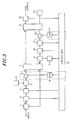
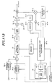
- the feed forward distortion compensation amplification apparatus includes two blocks: one is a distortion detection loop block including a directional coupler 1, a phase shifter 2, an amplitude adjuster 3, a pilot signal generator 4, a coupler 5 and a main amplifier 6; and the other is a distortion compensation loop block including a coupler 8, a detector 9, a phase shifter 10, an amplitude adjuster 11 and an error amplifier 12.
- the feed forward distortion compensation apparatus further includes dividers 7 and 13, a termination device 14, a coupler 15 and a control unit 18 for controlling each element of the feed forward distortion compensation amplification apparatus.
- the distortion detection loop block there exist two routes: one is a distortion-free route of a ⁇ c ⁇ e ⁇ g; and the other is a distortion route through a ⁇ b ⁇ d ⁇ f.
- the control unit 18 performs an automatic control on the phase shifter 2 and the amplitude adjuster 3 such that a received signal level of the distortion component measured by the detector 9 is minimized.
- ADP technique Another widely employed technique for achieving a good linearity in an amplification apparatus is an adaptive pre-distortion compensation technique (hereinafter referred to as an ADP technique) using a digital signal processing scheme.
- the ADP technique in general can be classified as a radio signal input type and a base band signal input type. Referring to Figs. 16A and 16B, there are provided distortion compensation amplification apparatuses of such types.
- Fig. 16A shows a distortion compensation amplification apparatus of the radio signal input type.
- a radio signal is inputted to an input terminal 21 and is successively subjected to a delay circuit 22, a gain control circuit 23 and a phase control circuit 24 and then, amplified at a power amplifier 34.
- the amplified radio signal is outputted through a coupler 38.
- the input radio signal is also converted to a digital data signal by passing through a logarithmic amplifier (LOG AMP) 27 and an A/D converter 28-1, both of which are incorporated in a power meter 29.
- the digital data signal is provided to a data processing unit 30-1.
- LOG AMP logarithmic amplifier
- the amplified radio data signal outputted from the power amplifier 34 is delivered to a multiplier circuit 33-1 through the directional coupler 38 and combined with the local frequency 32-1 thereat.
- the coupled signal from the multiplier circuit 33-1 is then subjected to a band-pass filter 31 to have a limited frequency band.
- the signal with the limited frequency band is inputted to the data processing unit 30-1 through an A/D converter 28-2.
- the data processing unit 30-1 operates by an algorithm for minimizing a level of the signal passing through the band-pass filter 31, i.e., off-band spectrum components generated by non-linear distortion characteristics of the power amplifier 34.
- the data processing unit 30-1 refers to addresses of memory circuits 26-1 and 26-2 based on the digital data signal provided from the power meter 29 to thereby control the gain control circuit 23 and the phase control circuit 24 through D/A converters 25-1 and 25-2, respectively.
- the contents of the memory circuits 26-1 and 26-2 are determined on a trial and error basis such that the non-linear distortion of the power amplifier 34 becomes minimized.
- a conventional distortion compensation amplification apparatus of the base band signal input type Referring to Fig. 16B, there is provided a conventional distortion compensation amplification apparatus of the base band signal input type.
- Carrier offset circuits 35-1 to 35-4 serve to offset carrier frequencies against respective input digital channel data based on carrier information for each input channel.
- the carrier offset circuit may be implemented, for example, by a complex multiplier.
- the outputs from the carrier offset circuits 35-1 to 35-4 are provided to an adder 39, which generates, in response thereto, a combined base band signal to the complex multiplier 36 and a power meter 29.
- the complex multiplier 36 controls the phase and the amplitude of the combined base band signal. Thereafter, the thus processed base band signal is subjected to a D/A converter 25-4 and a quadrature amplitude modulation unit (hereinafter, a QAM-MOD) 37, successively, and, then, combined with a signal from a local oscillator 32-2 at a multiplier circuit 33-2. Subsequently, the combined signal is transferred as a radio signal to the power amplifier 34 to be amplified thereat and finally outputted through a directional coupler 38.
- a QAM-MOD quadrature amplitude modulation unit
- An algorithm for minimizing non-linear distortion of the power amplifier 34 controls, as in the earlier-described radio signal input type, the complex multiplier 36 based on a power level of the base band signal, to thereby adjust the phase and the amplitude of the base band signal. That is, a data processing unit 30-2 refers to an address of a memory circuit 26-4 based on power level of the base band signal obtained from the power meter 29 to thereby control the complex multiplier 36. The contents of the memory circuit 26-4 which stores complex control values are determined on a trial and error basis such that the non-linear distortion can be minimized.
- One way to cut the operation costs is to reduce the power consumption.
- a transmitter power amplifier of the base station consumes a considerable amount of power at a constant rate regardless of the relative strength of the output signal transmitted by the base station. For instance, in daytime, the RF output power level consumed for a normal traffic load is about 10 watts and DC prime power consumed by the transmitter power amplifier is about 80 to 100 watts. However, in the middle of nighttime when the traffic load becomes light, the RF output power level of the transmitter may be reduced in decrements down to, e.g., about 1 watt due to the power control conducted over the RF output signal as described above. However, since an operation bias point is fixed in the conventional power amplifier, the DC prime power consumed by the transmitter power amplifier in the nighttime is not reduced but still remains unchanged at about 80 to 100 watts as in the daytime.
- an object of the present invention to provide a distortion compensation amplification apparatus capable of lowering consumption power by way of bias control.
- a feed forward type distortion compensation amplification apparatus including: a distortion detection loop having a first phase shifter, a first amplitude adjuster and a main amplifier; a distortion compensation loop having a second phase shifter, a second amplitude adjuster and an error amplifier; means for canceling a first distortion element generated from the distortion detection loop by a second distortion element generated from the distortion compensation loop and generating an output signal; and a bias controller for controlling bias levels of the main amplifier and the error amplifier based on a level of the output signal.
- an adaptive pre-distortion type distortion compensation amplification apparatus including: a detection unit for detecting an input power level; a control unit for storing the input power level and a bias level corresponding thereto and generating the bias level in response to the input power level; and a bias control unit for applying a bias to an amplifier unit in response to the bias level.
- a distortion compensation amplification apparatus including: a detection unit for detecting a level of an input signal; an amplification unit for amplifying the input signal; and means for stepwise controlling a bias of the amplification unit based on the level of the input signal detected by the detection unit.
- a distortion compensation amplification apparatus including: an amplification unit for amplifying an input signal; a detection unit for detecting a level of an output signal; and means for controlling a bias of the amplification unit based on the level of the output signal detected by the detection unit.
- inventive features of the present invention can be realized by any other circuits or apparatus than those described in the preferred embodiments of the invention as long as they can realize such features. Further, some or all of the functions thereof may be implemented by software. In addition, each of certain functional elements of the system can be implemented by a plurality of circuits or a multiplicity of such functional elements thereof can be configured by a single circuit.
- class AB amplifiers or class B amplifiers are generally used.
- Such amplifiers have characteristics that power consumption level decreases with the reduction of the output power level, as shown in Fig. 1. Since, however, an idle current needs to be set in such an amplifier, the power consumption level of the amplifier may not be reduced below a predetermined power level corresponding to the idle current of the amplifier.
- an ACLR Adjacent Channel Leakage power Ratio
- conventional main and error amplifier exhibit a large ACRL margin for a wireless standard level at a low output power level, as can be seen from an ACLR curve represented by a solid line shown in Fig. 2. Since an amplifier would need to satisfy the wireless characteristics, a bias control for the main and the error amplifier can be performed when the amplifiers operate, particularly, at a low output power level, in accordance with the present invention as represented by a dashed line in Fig. 2. The detailed explanation thereof will be described hereinafter.
- Fig. 3 shows a block diagram of a distortion compensation amplification apparatus using a feed forward technique in accordance with a first preferred embodiment of the present invention. Since some elements of the distortion compensation amplification apparatus in Fig. 3 are identical to those of the conventional distortion compensation amplification apparatus shown in Fig. 15, the same reference numerals are used to denote and identify corresponding or identical elements of the conventional distortion compensation conventional amplification apparatus, and the detailed description thereof will be omitted.
- a main amp bias control circuit 16 performs a bias control of a main amplifier 6 and an error amp bias control circuit 17 performs a bias control on an error amplifier 12.
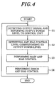
- a coupler 15 reports a power level of the output signal to a control unit 18 at step S1.
- the control unit 18, which stores in its memory (not shown) bias levels for the main amplifier 6 and the error amplifier 12 as a function of output power level as shown in Fig. 5, retrieves a main amp bias level for the main amplifier 6 and an error amp bias level for the error amplifier 12 in response to the output power level at step S2.
- the main amp bias control circuit 16 Based on the retrieved main amp bias level, the main amp bias control circuit 16 performs a bias control on the main amplifier 6 at step S3 and, further, based on the retrieved error amp bias level, the error amp bias control circuit 17 performs a bias control on the error amplifier 12 at step S4.
- a memory table defined in the memory of the control unit 18 specifies, e.g., three output power levels A, B and C of the amplification apparatus and their corresponding main amp bias levels and error amp bias levels.
- a relationship between bias levels for an amplifier and output power levels will be described in detail with reference to Figs. 6 and 7.
- Fig. 6 the relationship between a main amp bias level of the main amplifier 6 and an output power level of the amplification apparatus with and without a bias control is described in Fig. 6.
- the abscissa represents an output power level
- the right ordinate represents a main amp bias level
- the left ordinate represents a consumption current of the main amplifier 6.
- Dashed lines and solid lines respectively represent the cases with and without bias control.
- the main amp bias levels with and without bias control are identical to be A' and therefore the consumption currents also become equal.
- the output power level is B
- the applied main amp bias level with bias control is reduced down to the level B' and the consumption current of the main amplifier 6 in the bias control state becomes smaller than that of the main amplifier 6 in the bias fixed state.
- the output power level is the lowest output power level C
- the main amp bias level in the bias control state becomes the level C', being lower than B', and the current consumption of the main amplifier 6 in the bias control state becomes further decreased as shown in Fig. 6.
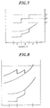
- Fig. 7 provides graphs for illustrating the relationship between an error amp bias level of the error amplifier 12 and an output power level of the amplification apparatus with and without bias control.
- the abscissa represents an output power level
- the right ordinate represents an error amp bias level
- the left ordinate represents a consumption current of the error amplifier 12.
- Dashed lines and solid lines respectively represent the cases with and without a bias control.
- the output power level is high (level A)
- the error amp bias levels with and without bias control are identical to A" and therefore the consumption currents also become equal.
- the output power level is B
- the applied error amp bias level with bias control is reduced down to the level B" and the consumption current of the error amplifier 12 in the bias control state becomes smaller than that of the error amplifier 12 in the bias fixed state.
- the output power level is the lowest output power level C
- the error amp bias level in the bias control state becomes the level C", being lower than B"
- the current consumption of the error amplifier 12 in the bias control state becomes further decreased as shown in Fig. 7.
- Fig. 8 depicts a graph for illustrating an ACLR and a consumption power of the amplification apparatus as a function of an output power level with and without bias control.
- the abscissa represents an output power level
- the right ordinate represents consumption power
- the left ordinate represents an ACLR.
- Dashed lines and solid lines respectively represent the cases with and without a bias control.
- the output power levels are divided into three levels A, B and C. It should be noted, however, that the output power levels can be more finely divided, even into, e.g., non-discrete continuous levels. Such case is represented as, for example, dashed curves shown in Figs. 1 and 2.
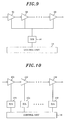
- Figs. 9 and 10 represent bias control blocks for bias control of amplifiers in accordance with the present invention.
- the bias control blocks correspond to a dashed block having the main amplifier 6, the main amp bias control circuit 16 and the control unit 18 or a dashed block having the error amplifier 12, the error amp bias control circuit 17 and the control unit 18 in the amplification apparatus of Fig. 3.
- the amplifiers in the bias control blocks can be configured with a plurality of main amplifier units or error amplifier units as shown in Figs. 9 and 10.
- a plurality of amplifier units 91-93 in the bias control block are controlled by a single amp bias control circuit 94.
- the amplifier is constructed with cascaded small-power amplifier unit 91, medium-power amplifier unit 92 and large-power amplifier unit 93.
- bias control corresponding to an output power level can be performed for the amplifier units 91, 92 and 93 by only a single amp bias control circuit 94.
- Fig. 10 sets forth a bias control block including a plurality of amplifier units and the same number of amp bias control circuits.
- the amplifier is constructed with a small-power amplifier unit 101, a medium-power amplifier unit 102 and a large-power amplifier unit 103.
- bias control corresponding to an output power level can be performed for each of the amplifier units 101, 102 and 103 by its corresponding amp bias control circuits 104, 105 or 106, enabling independent bias control to be performed for each of the amplifier units.
- efficient power saving can be achieved by fixing a bias level of a small-power amplifier unit and performing bias controls of a medium-power amplifier unit and a large-power amplifier unit.
- the amplifier units and the amp bias control circuits are shown in Figs. 9 and 10 to be of a one-to-one correspondence or a multi-to-one correspondence, it should be noted, that the number of bias control circuits can be varied.
- the bias control block can be configured in such a manner that more than one, but not greater than the number of amplifier units, bias control circuit performs bias controls of the amplifier blocks.
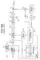
- Fig. 11A shows a block diagram of a distortion compensation amplification apparatus in accordance with a second preferred embodiment of the present invention, which uses the ADP (adaptive pre-distortion compensation) technique with an RF signal input.
- Fig. 11B shows a block diagram of a distortion compensation amplification apparatus in accordance with a third preferred embodiment of the present invention, which uses the ADP technique with a base band signal input.
- Both of the distortion compensation amplification apparatuses as shown in Figs. 11A and 11B further include a memory 26-3 and a D/A converter 25-3 for performing a bias control of a power amplifier 34 in comparison with the conventional distortion compensation amplification apparatuses as shown in Figs. 16A and 16B.
- the distortion compensation amplification apparatuses of the second and the third embodiment perform a bias control such that a bias level is optimized while satisfying the wireless characteristics, e.g., ACLR, especially at the region of low output power levels having a large margin with respect to the wireless standard.
- the wireless characteristics e.g., ACLR
- Fig. 12 offers a flow chart illustrating a process for performing bias controls for the power amplifier 34 shown in each of Figs. 11A and 11B.
- a gain control and a phase control corresponding to the input power level are performed at step S20 and a bias control corresponding to the input power level is performed at step S30.
- the ACLR increases and its margin for the wireless standard decreases as the output power level goes near a maximum rated level. Since the output power level increases in proportion to input power level, the ADP technique can capture an output power level by monitoring the input power level and thereby can reduce the amount of consumption current of the amplification apparatus in such a manner that ACLR falls within the wireless standard level at low output power levels.
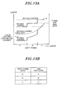
- Fig. 13A which corresponds to Fig. 6, presents a graph for illustrating a relationship of a bias level and consumption current of the power amplifier 34 versus an input power level of the amplification apparatus with and without bias control.
- Fig. 13B is a memory table for specifying input power levels of the amplification apparatus and power amp bias levels, which are stored in the memory 26-3.
- the input power levels are divided into three levels of A, B and C.
- consumption current can be reduced more smoothly without abrupt large variations.
- consumption current of 5.6 A RMS root-mean-square
- RMS root-mean-square
- Fig. 14 which corresponds to Fig. 8, depicts a graph for illustrating a relationship of an ACLR and a consumption power of a power amplifier versus an input power level of the amplification apparatus with and without bias control.
- the ACLR in a bias control state is degraded in comparison with that in a bias fixed state. However, in both levels B and C, the ACLR in a bias control state is still maintained within the wireless standard.
- the power amplifier 34 can be implemented by a plurality of amplifier units whose bias levels are collectively or separately controlled in a similar manner as in Fig. 9 or 10.
- the present invention has been described with respect to the CDMA communications system. It should be noted, however, that the present invention can be equally applied in controlling amplifiers of base stations of other types of communications system, e.g., TDMA communications system, which consume powers without employing bias control.
Landscapes
- Engineering & Computer Science (AREA)
- Power Engineering (AREA)
- Physics & Mathematics (AREA)
- Nonlinear Science (AREA)
- Amplifiers (AREA)
Applications Claiming Priority (4)
| Application Number | Priority Date | Filing Date | Title |
|---|---|---|---|
| JP2001239839A JP3761076B2 (ja) | 2001-08-07 | 2001-08-07 | フィードフォワード方式歪補償増幅器 |
| JP2001239839 | 2001-08-07 | ||
| JP2002058239A JP2003258563A (ja) | 2002-03-05 | 2002-03-05 | プリディストーション方式歪み補償増幅装置 |
| JP2002058239 | 2002-03-05 |
Publications (1)
| Publication Number | Publication Date |
|---|---|
| EP1289127A2 true EP1289127A2 (fr) | 2003-03-05 |
Family
ID=26620138
Family Applications (1)
| Application Number | Title | Priority Date | Filing Date |
|---|---|---|---|
| EP02009684A Withdrawn EP1289127A2 (fr) | 2001-08-07 | 2002-04-29 | Dispositif amplificateur de compensation de distorsion par contre-réaction du type aval et par prédistorsion adaptative |
Country Status (4)
| Country | Link |
|---|---|
| US (2) | US6756844B2 (fr) |
| EP (1) | EP1289127A2 (fr) |
| KR (1) | KR100786456B1 (fr) |
| CN (1) | CN1266830C (fr) |
Cited By (3)
| Publication number | Priority date | Publication date | Assignee | Title |
|---|---|---|---|---|
| EP1594222A1 (fr) * | 2004-05-07 | 2005-11-09 | Alcatel | Procédé d'ajustage du point de fonctionnement et circuit amplificateur de puissance |
| EP2102992A4 (fr) * | 2006-12-21 | 2011-05-11 | Icera Canada ULC | Commande de puissance numérique en boucle fermée pour un émetteur sans fil |
| US8520770B2 (en) | 2008-06-19 | 2013-08-27 | Fujitsu Limited | Amplitude suppressing apparatus and signal transmitting apparatus |
Families Citing this family (22)
| Publication number | Priority date | Publication date | Assignee | Title |
|---|---|---|---|---|
| US6985706B2 (en) * | 2003-01-23 | 2006-01-10 | Powerwave Technologies, Inc. | Feed forward amplifier system employing self-generating alignment lists and adaptive controller |
| WO2004112242A1 (fr) * | 2003-06-18 | 2004-12-23 | Koninklijke Philips Electronics N.V. | Amplificateur de puissance avec boucle de reglage de la puissance |
| DE50311519D1 (de) * | 2003-07-17 | 2009-06-25 | Palm Inc | Schaltungsanordnung und Verfahren zur Erhöhung des Wirkungsgrades eines Leistungsverstärkers |
| WO2005050831A1 (fr) * | 2003-10-20 | 2005-06-02 | Thomson Licensing | Generateur de predistorsion pour emetteur sans fil |
| JP3999232B2 (ja) * | 2004-04-07 | 2007-10-31 | 株式会社日立国際電気 | 増幅装置 |
| EP1601096A1 (fr) * | 2004-05-27 | 2005-11-30 | Alcatel | Procédé et circuit de boucle électronique pour ajuster la tension de polarisation |
| US7190221B2 (en) * | 2004-10-22 | 2007-03-13 | Nokia Corporation | Method and apparatus for maintaining constant linearity for a power amplifier over varying load conditions |
| US7221222B2 (en) * | 2005-07-28 | 2007-05-22 | Motorola, Inc. | Methods and apparatus of managing a power amplifier |
| US7221223B2 (en) * | 2005-07-28 | 2007-05-22 | Motorola, Inc. | Methods and apparatus of managing a power amplifier |
| US8019015B2 (en) * | 2007-02-26 | 2011-09-13 | Harris Corporation | Linearization of RF power amplifiers using an adaptive subband predistorter |
| US11036262B1 (en) * | 2008-01-14 | 2021-06-15 | Micro Mobio Corporation | Radio frequency power amplifier with adjacent channel leakage correction circuit |
| JP5052366B2 (ja) * | 2008-02-20 | 2012-10-17 | 株式会社エヌ・ティ・ティ・ドコモ | 高効率フィードフォワード増幅器の制御方法 |
| US7957705B1 (en) | 2008-03-18 | 2011-06-07 | Sprint Spectrum L.P. | System and method for reducing radio frequency interference caused by a carrier |
| US7642850B2 (en) * | 2008-04-02 | 2010-01-05 | Harris Corporation | Feedforward linearization of RF power amplifiers |
| DE102008052172B4 (de) * | 2008-10-17 | 2014-01-23 | Fraunhofer-Gesellschaft zur Förderung der angewandten Forschung e.V. | Vorrichtung zum Erzeugen eines Korrektursignals |
| KR101046350B1 (ko) * | 2008-10-30 | 2011-07-05 | 장세주 | 간섭억제시스템 필터모듈 기반 전치왜곡장치 및 적응형 피드포워드 선형화회로가 적용된 이동통신장치의 출력단 |
| US7944293B2 (en) * | 2008-12-11 | 2011-05-17 | Samsung Electro-Mechanics Company, Ltd. | Systems and methods for an adaptive bias circuit for a differential power amplifier |
| US8401400B2 (en) * | 2009-03-10 | 2013-03-19 | Tyco Electronics Subsea Communications Llc | Detection of data in signals with data pattern dependent signal distortion |
| US20110250853A1 (en) * | 2010-04-09 | 2011-10-13 | Andrea Camuffo | Operating point setting of an amplifier |
| CN103401513B (zh) * | 2013-08-02 | 2016-02-10 | 武汉邮电科学研究院 | 一种功率放大器的数字预失真处理方法和装置 |
| US12463322B1 (en) | 2019-04-03 | 2025-11-04 | Micro Mobio Corporation | Antenna in display |
| US11515617B1 (en) | 2019-04-03 | 2022-11-29 | Micro Mobio Corporation | Radio frequency active antenna system in a package |
Family Cites Families (18)
| Publication number | Priority date | Publication date | Assignee | Title |
|---|---|---|---|---|
| JPH0548346A (ja) | 1991-08-20 | 1993-02-26 | Oki Electric Ind Co Ltd | 線形化電力増幅回路 |
| FR2716313B1 (fr) | 1994-02-11 | 1996-04-12 | Alcatel Mobile Comm France | Dispositif de commande de la polarisation d'un amplificateur. |
| JP3529439B2 (ja) * | 1994-08-10 | 2004-05-24 | 株式会社日立国際電気 | 歪補償増幅回路とその補償最適化方法 |
| JPH08125469A (ja) * | 1994-10-21 | 1996-05-17 | Nec Corp | 電力増幅器の出力制御装置 |
| US5787336A (en) * | 1994-11-08 | 1998-07-28 | Space Systems/Loral, Inc. | Satellite communication power management system |
| JP2788865B2 (ja) | 1995-03-20 | 1998-08-20 | 福島日本電気株式会社 | 歪補償器 |
| US5923215A (en) * | 1996-06-13 | 1999-07-13 | The Whitaker Corporation | Linearized amplifier |
| US5757229A (en) * | 1996-06-28 | 1998-05-26 | Motorola, Inc. | Bias circuit for a power amplifier |
| JP3553308B2 (ja) * | 1997-02-17 | 2004-08-11 | 株式会社日立国際電気 | 歪補償増幅器 |
| US6223056B1 (en) | 1997-12-31 | 2001-04-24 | Samsung Electronics Co., Ltd. | Systems and methods for dynamically controlling a variable power amplifier |
| US6028477A (en) * | 1998-04-08 | 2000-02-22 | Powerwave Technologies, Inc. | Adaptive biasing in a power amplifier |
| JP2000151295A (ja) * | 1998-11-05 | 2000-05-30 | Mitsubishi Electric Corp | 歪補償回路 |
| US6320464B1 (en) * | 1999-03-13 | 2001-11-20 | Ntt Mobile Communications Network, Inc. | Feedforward amplifier |
| JP3389142B2 (ja) | 1999-04-30 | 2003-03-24 | エヌイーシーモバイリング株式会社 | 負帰還型歪み補償回路 |
| US6396350B2 (en) * | 2000-02-09 | 2002-05-28 | Paradigm Wireless Systems, Inc. | Power booster method and apparatus for improving the performance of radio frequency linear power amplifiers |
| JP2001223541A (ja) * | 2000-02-09 | 2001-08-17 | Nec Corp | フィードフォワード増幅器 |
| US6388526B1 (en) * | 2000-07-06 | 2002-05-14 | Lucent Technologies Inc. | Methods and apparatus for high performance reception of radio frequency communication signals |
| US6496064B2 (en) * | 2000-08-15 | 2002-12-17 | Eugene Rzyski | Intermodulation product cancellation circuit |
-
2002
- 2002-04-23 US US10/127,568 patent/US6756844B2/en not_active Expired - Fee Related
- 2002-04-29 EP EP02009684A patent/EP1289127A2/fr not_active Withdrawn
- 2002-05-09 CN CNB021191395A patent/CN1266830C/zh not_active Expired - Fee Related
- 2002-05-17 KR KR1020020027268A patent/KR100786456B1/ko not_active Expired - Fee Related
-
2004
- 2004-06-01 US US10/857,017 patent/US20040217811A1/en not_active Abandoned
Cited By (4)
| Publication number | Priority date | Publication date | Assignee | Title |
|---|---|---|---|---|
| EP1594222A1 (fr) * | 2004-05-07 | 2005-11-09 | Alcatel | Procédé d'ajustage du point de fonctionnement et circuit amplificateur de puissance |
| EP2102992A4 (fr) * | 2006-12-21 | 2011-05-11 | Icera Canada ULC | Commande de puissance numérique en boucle fermée pour un émetteur sans fil |
| US8509290B2 (en) | 2006-12-21 | 2013-08-13 | Icera Canada ULC | Closed-loop digital power control for a wireless transmitter |
| US8520770B2 (en) | 2008-06-19 | 2013-08-27 | Fujitsu Limited | Amplitude suppressing apparatus and signal transmitting apparatus |
Also Published As
| Publication number | Publication date |
|---|---|
| CN1405976A (zh) | 2003-03-26 |
| KR100786456B1 (ko) | 2007-12-17 |
| CN1266830C (zh) | 2006-07-26 |
| US6756844B2 (en) | 2004-06-29 |
| US20030030490A1 (en) | 2003-02-13 |
| US20040217811A1 (en) | 2004-11-04 |
| KR20030013238A (ko) | 2003-02-14 |
Similar Documents
| Publication | Publication Date | Title |
|---|---|---|
| US6756844B2 (en) | Distortion compensation amplification apparatus of feed forward type and adaptive pre-distortion type | |
| KR100703649B1 (ko) | Rf 전력 증폭기의 동적 바이어스를 위한 가입자 장치 및방법 | |
| US6591090B1 (en) | Predistortion control for power reduction | |
| JP4101177B2 (ja) | プレディストーション誤差補正を有する広帯域線形増幅器 | |
| US7888997B2 (en) | Systems, methods, and apparatuses for linear envelope elimination and restoration transmitters | |
| JP4203968B2 (ja) | 無線送信器に関する装置および方法 | |
| JP2002232325A (ja) | プリディストーション歪み補償装置 | |
| KR100363403B1 (ko) | 궤환기법을 응용한 실시간 자력적/적응성 간섭잡음제거장치 및 그 방법 | |
| US6711217B1 (en) | Apparatus and method for linearized power amplification | |
| JPH09135127A (ja) | 電力増幅器 | |
| EP1451925A1 (fr) | Amplificateur composite | |
| US7688156B2 (en) | Polar modulation transmission circuit and communication device | |
| GB2337169A (en) | An adaptive predistorter for an amplifier | |
| JP3643803B2 (ja) | 増幅装置 | |
| KR980012970A (ko) | 전력 소모가 적고 회로 크기가 작은 송신 장치 | |
| EP1437825B1 (fr) | Annulation de produit d'intermodulation dans des systèmes de communication | |
| JP2001274633A (ja) | 電力増幅装置 | |
| JP2002290166A (ja) | 増幅装置 | |
| GB2592678A (en) | Amplifier and amplification method | |
| JP3578958B2 (ja) | 増幅装置 | |
| JP4030319B2 (ja) | フィードフォワード非線形歪補償増幅器 | |
| KR100375314B1 (ko) | 선형 특성을 개선시킨 통신 시스템 및 그 제어 방법 | |
| JP2001244751A (ja) | 電力増幅器 | |
| JP3495283B2 (ja) | フィードフォワード型増幅器及びこれを用いた無線通信装置 | |
| JP2004343496A (ja) | 非線型歪補償回路を用いた送信機 |
Legal Events
| Date | Code | Title | Description |
|---|---|---|---|
| PUAI | Public reference made under article 153(3) epc to a published international application that has entered the european phase |
Free format text: ORIGINAL CODE: 0009012 |
|
| AK | Designated contracting states |
Kind code of ref document: A2 Designated state(s): AT BE CH CY DE DK ES FI FR GB GR IE IT LI LU MC NL PT SE TR Designated state(s): AT BE CH CY DE DK ES FI FR GB GR IE IT LI LU MC NL PT SE TR |
|
| AX | Request for extension of the european patent |
Extension state: AL LT LV MK RO SI |
|
| STAA | Information on the status of an ep patent application or granted ep patent |
Free format text: STATUS: THE APPLICATION IS DEEMED TO BE WITHDRAWN |
|
| 18D | Application deemed to be withdrawn |
Effective date: 20041102 |