EP1291917A2 - Elément de circuit électrique, notamment des modules à haut prestation et procès de fabrication associée - Google Patents
Elément de circuit électrique, notamment des modules à haut prestation et procès de fabrication associée Download PDFInfo
- Publication number
- EP1291917A2 EP1291917A2 EP02019744A EP02019744A EP1291917A2 EP 1291917 A2 EP1291917 A2 EP 1291917A2 EP 02019744 A EP02019744 A EP 02019744A EP 02019744 A EP02019744 A EP 02019744A EP 1291917 A2 EP1291917 A2 EP 1291917A2
- Authority
- EP
- European Patent Office
- Prior art keywords
- conductor structure
- circuit unit
- unit according
- electrical
- stamped part
- Prior art date
- Legal status (The legal status is an assumption and is not a legal conclusion. Google has not performed a legal analysis and makes no representation as to the accuracy of the status listed.)
- Withdrawn
Links
Images



Classifications
-
- H—ELECTRICITY
- H01—ELECTRIC ELEMENTS
- H01R—ELECTRICALLY-CONDUCTIVE CONNECTIONS; STRUCTURAL ASSOCIATIONS OF A PLURALITY OF MUTUALLY-INSULATED ELECTRICAL CONNECTING ELEMENTS; COUPLING DEVICES; CURRENT COLLECTORS
- H01R43/00—Apparatus or processes specially adapted for manufacturing, assembling, maintaining, or repairing of line connectors or current collectors or for joining electric conductors
- H01R43/20—Apparatus or processes specially adapted for manufacturing, assembling, maintaining, or repairing of line connectors or current collectors or for joining electric conductors for assembling or disassembling contact members with insulating base, case or sleeve
- H01R43/24—Assembling by moulding on contact members
-
- H—ELECTRICITY
- H05—ELECTRIC TECHNIQUES NOT OTHERWISE PROVIDED FOR
- H05K—PRINTED CIRCUITS; CASINGS OR CONSTRUCTIONAL DETAILS OF ELECTRIC APPARATUS; MANUFACTURE OF ASSEMBLAGES OF ELECTRICAL COMPONENTS
- H05K3/00—Apparatus or processes for manufacturing printed circuits
- H05K3/10—Apparatus or processes for manufacturing printed circuits in which conductive material is applied to the insulating support in such a manner as to form the desired conductive pattern
- H05K3/20—Apparatus or processes for manufacturing printed circuits in which conductive material is applied to the insulating support in such a manner as to form the desired conductive pattern by affixing prefabricated conductor pattern
- H05K3/202—Apparatus or processes for manufacturing printed circuits in which conductive material is applied to the insulating support in such a manner as to form the desired conductive pattern by affixing prefabricated conductor pattern using self-supporting metal foil pattern
-
- H—ELECTRICITY
- H10—SEMICONDUCTOR DEVICES; ELECTRIC SOLID-STATE DEVICES NOT OTHERWISE PROVIDED FOR
- H10W—GENERIC PACKAGES, INTERCONNECTIONS, CONNECTORS OR OTHER CONSTRUCTIONAL DETAILS OF DEVICES COVERED BY CLASS H10
- H10W40/00—Arrangements for thermal protection or thermal control
- H10W40/10—Arrangements for heating
-
- H—ELECTRICITY
- H10—SEMICONDUCTOR DEVICES; ELECTRIC SOLID-STATE DEVICES NOT OTHERWISE PROVIDED FOR
- H10W—GENERIC PACKAGES, INTERCONNECTIONS, CONNECTORS OR OTHER CONSTRUCTIONAL DETAILS OF DEVICES COVERED BY CLASS H10
- H10W70/00—Package substrates; Interposers; Redistribution layers [RDL]
- H10W70/40—Leadframes
- H10W70/479—Leadframes on or in insulating or insulated package substrates, interposers, or redistribution layers
-
- H—ELECTRICITY
- H10—SEMICONDUCTOR DEVICES; ELECTRIC SOLID-STATE DEVICES NOT OTHERWISE PROVIDED FOR
- H10W—GENERIC PACKAGES, INTERCONNECTIONS, CONNECTORS OR OTHER CONSTRUCTIONAL DETAILS OF DEVICES COVERED BY CLASS H10
- H10W76/00—Containers; Fillings or auxiliary members therefor; Seals
- H10W76/10—Containers or parts thereof
- H10W76/12—Containers or parts thereof characterised by their shape
- H10W76/15—Containers comprising an insulating or insulated base
- H10W76/157—Containers comprising an insulating or insulated base having interconnections parallel to the insulating or insulated base
-
- H—ELECTRICITY
- H01—ELECTRIC ELEMENTS
- H01R—ELECTRICALLY-CONDUCTIVE CONNECTIONS; STRUCTURAL ASSOCIATIONS OF A PLURALITY OF MUTUALLY-INSULATED ELECTRICAL CONNECTING ELEMENTS; COUPLING DEVICES; CURRENT COLLECTORS
- H01R13/00—Details of coupling devices of the kinds covered by groups H01R12/70 or H01R24/00 - H01R33/00
- H01R13/66—Structural association with built-in electrical component
- H01R13/665—Structural association with built-in electrical component with built-in electronic circuit
-
- H—ELECTRICITY
- H01—ELECTRIC ELEMENTS
- H01R—ELECTRICALLY-CONDUCTIVE CONNECTIONS; STRUCTURAL ASSOCIATIONS OF A PLURALITY OF MUTUALLY-INSULATED ELECTRICAL CONNECTING ELEMENTS; COUPLING DEVICES; CURRENT COLLECTORS
- H01R31/00—Coupling parts supported only by co-operation with counterpart
- H01R31/06—Intermediate parts for linking two coupling parts, e.g. adapter
- H01R31/065—Intermediate parts for linking two coupling parts, e.g. adapter with built-in electric apparatus
-
- H—ELECTRICITY
- H01—ELECTRIC ELEMENTS
- H01R—ELECTRICALLY-CONDUCTIVE CONNECTIONS; STRUCTURAL ASSOCIATIONS OF A PLURALITY OF MUTUALLY-INSULATED ELECTRICAL CONNECTING ELEMENTS; COUPLING DEVICES; CURRENT COLLECTORS
- H01R43/00—Apparatus or processes specially adapted for manufacturing, assembling, maintaining, or repairing of line connectors or current collectors or for joining electric conductors
- H01R43/16—Apparatus or processes specially adapted for manufacturing, assembling, maintaining, or repairing of line connectors or current collectors or for joining electric conductors for manufacturing contact members, e.g. by punching and by bending
-
- H—ELECTRICITY
- H05—ELECTRIC TECHNIQUES NOT OTHERWISE PROVIDED FOR
- H05K—PRINTED CIRCUITS; CASINGS OR CONSTRUCTIONAL DETAILS OF ELECTRIC APPARATUS; MANUFACTURE OF ASSEMBLAGES OF ELECTRICAL COMPONENTS
- H05K2201/00—Indexing scheme relating to printed circuits covered by H05K1/00
- H05K2201/09—Shape and layout
- H05K2201/09009—Substrate related
- H05K2201/09118—Moulded substrate
-
- H—ELECTRICITY
- H05—ELECTRIC TECHNIQUES NOT OTHERWISE PROVIDED FOR
- H05K—PRINTED CIRCUITS; CASINGS OR CONSTRUCTIONAL DETAILS OF ELECTRIC APPARATUS; MANUFACTURE OF ASSEMBLAGES OF ELECTRICAL COMPONENTS
- H05K3/00—Apparatus or processes for manufacturing printed circuits
- H05K3/0058—Laminating printed circuit boards onto other substrates, e.g. metallic substrates
- H05K3/0061—Laminating printed circuit boards onto other substrates, e.g. metallic substrates onto a metallic substrate, e.g. a heat sink
-
- H—ELECTRICITY
- H05—ELECTRIC TECHNIQUES NOT OTHERWISE PROVIDED FOR
- H05K—PRINTED CIRCUITS; CASINGS OR CONSTRUCTIONAL DETAILS OF ELECTRIC APPARATUS; MANUFACTURE OF ASSEMBLAGES OF ELECTRICAL COMPONENTS
- H05K3/00—Apparatus or processes for manufacturing printed circuits
- H05K3/30—Assembling printed circuits with electric components, e.g. with resistors
- H05K3/32—Assembling printed circuits with electric components, e.g. with resistors electrically connecting electric components or wires to printed circuits
- H05K3/321—Assembling printed circuits with electric components, e.g. with resistors electrically connecting electric components or wires to printed circuits by conductive adhesives
Definitions
- the present invention relates to an electrical circuit unit, in particular a power module and a process for their production.
- the invention has for its object an electrical circuit unit and in particular to specify a power module that is advantageous Has structure and is therefore inexpensive to manufacture. About that In addition, an advantageous method for producing such Circuit unit can be specified.
- an electrical circuit unit in particular Power module with one of at least one metal stamped part formed conductor structure, the conductor structure at least partially in a solid insulation material is embedded.
- At least one metal stamped part as a conductor structure can be a relatively large cross-section of the conductor in an inexpensive manner can be achieved.
- At least one electrical component, in particular power element, provided with a side designed as an electrical connection to the metal stamped part is put on.
- the metal stamped part serves directly as a connecting line for the electrical component.
- the metal stamped part also works due to the flat connection with the electrical component as an effective heat dissipation.
- the component can act, for example, a chip, in particular a MOSFET.
- the conductor structure for electrical energy supply can be particularly advantageous of the electrical components are used.
- By the possible large cross-section of the conductor structure can easily also high Currents, for example in the range of 60 amperes, are transmitted, without the conductor structure itself generating large amounts of heat. Much more it can be effective for heat dissipation due to its thermal conductivity contribute.
- the insulating material forms a support surface for a circuit carrier on one side of the conductor structure.
- Components can thereby advantageously further electrical Components are integrated into the circuit unit according to the invention.
- the circuit carrier is preferably also on the one facing the support surface Provide side with electrical components.
- the support surface can for this, in particular at least one recess for receiving electrical Have components of the circuit carrier. the components are protected.
- the conductor structure is kept free of insulating material.
- a heat sink with the conductor structure is thermally connected. This can optimize heat dissipation become.
- a heat-conducting, heat-conducting, electrically insulating layer provided. It can be a slide or trade an adhesive. This creates good thermal contact guaranteed between the heat sink and the conductor structure.
- circuit carrier side of the circuit unit with a Cover.
- the lid protects the entire unit.
- Figure 1 shows a metallic lead frame 1, which extends in two planes Tracks 2 includes.
- the lead frame 1 is in a connector housing, So-called header inserted, which additionally with the metal punched grille on the side 1 extending busbar 4 is provided.
- the metal punched grid 1 is then, as shown in Figures 2 and 3, overmolded with insulating material 5 such that the metal punched grid 1 remains free of insulating material on one side while on the other Side a support surface 6 is formed for a circuit carrier.
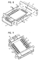
- a heat sink 7 is then applied according to FIG. For this, is on the heat sink 7 applied thermal adhesive or it is with a Heat-conducting film stuck on before it is placed on the metal punched grid 1 becomes.
- a support surface 6 is formed Printed circuit board 8 applied as a circuit carrier with other components.
- the components are also on the support surface 6 facing side. These are from a recess 6 'in the support surface 6 added.
- the connection between circuit board 8 and support surface 6 is preferably carried out by previously applied to the support surface 6 Glue.
- the sections of the metal stamped grid located next to the printed circuit board 8 1 are also kept free of insulating material.
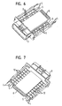
- points 9 of electrical connection material, in particular Conductive adhesive applied.
- electrical components 10 with a side serving as an electrical connection, in particular MOSFET, on the sections of the points 9 Metal punched grid 1 is placed, as shown in Figure 7.
- FIG. 9 shows the establishment of the electrical connections 14 (bonding) between the MOSFET 10 and the circuit board 8 as well the MOSFET 10 and the metal punched grid 1.
- a circuit unit is thus obtained, in particular as a power module can be used.
- a metal stamped grid 1 high wire cross sections can be achieved without a costly lamination process must be used.
- the embedding in electrical insulating material 5 enables high mechanical Stability of unity.
- the insulating material 5 advantageously forms a support surface 6 for a printed circuit board 8 with further components, so that a complex module can be represented overall. Yet Overall, the manufacture remains relatively simple and inexpensive.
Landscapes
- Engineering & Computer Science (AREA)
- Manufacturing & Machinery (AREA)
- Microelectronics & Electronic Packaging (AREA)
- Structure Of Printed Boards (AREA)
- Insulated Metal Substrates For Printed Circuits (AREA)
- Cooling Or The Like Of Semiconductors Or Solid State Devices (AREA)
Applications Claiming Priority (2)
| Application Number | Priority Date | Filing Date | Title |
|---|---|---|---|
| DE10144323A DE10144323A1 (de) | 2001-09-10 | 2001-09-10 | Elektrische Schaltungseinheit, insbesondere Leistungsmodul, und Verfahren zur deren Herstellung |
| DE10144323 | 2001-09-10 |
Publications (2)
| Publication Number | Publication Date |
|---|---|
| EP1291917A2 true EP1291917A2 (fr) | 2003-03-12 |
| EP1291917A3 EP1291917A3 (fr) | 2005-10-19 |
Family
ID=7698355
Family Applications (1)
| Application Number | Title | Priority Date | Filing Date |
|---|---|---|---|
| EP02019744A Withdrawn EP1291917A3 (fr) | 2001-09-10 | 2002-09-03 | Elément de circuit électrique, notamment des modules à haut prestation et procès de fabrication associée |
Country Status (2)
| Country | Link |
|---|---|
| EP (1) | EP1291917A3 (fr) |
| DE (1) | DE10144323A1 (fr) |
Cited By (1)
| Publication number | Priority date | Publication date | Assignee | Title |
|---|---|---|---|---|
| FR2913538A1 (fr) * | 2007-03-05 | 2008-09-12 | Peugeot Citroen Automobiles Sa | Gel d'isolation en plaque pour isolation renforcee. |
Families Citing this family (2)
| Publication number | Priority date | Publication date | Assignee | Title |
|---|---|---|---|---|
| DE10323170A1 (de) * | 2003-05-22 | 2004-12-09 | Conti Temic Microelectronic Gmbh | Stecker mit Elektronikschaltung |
| DE102006031389A1 (de) * | 2006-07-07 | 2008-01-10 | Danfoss Bauer Gmbh | Anschlußleitung |
Family Cites Families (6)
| Publication number | Priority date | Publication date | Assignee | Title |
|---|---|---|---|---|
| US5212627A (en) * | 1992-01-31 | 1993-05-18 | Motorola, Inc. | Electronic module housing and assembly with integral heatsink |
| DE19544974C1 (de) * | 1995-12-01 | 1997-05-22 | Siemens Ag | Steuergerät, insbesondere zur Auslösung eines Rückhaltemittels in einem Fahrzeug |
| US6281579B1 (en) * | 1997-02-14 | 2001-08-28 | International Rectifier Corporation | Insert-molded leadframe to optimize interface between powertrain and driver board |
| JPH11233712A (ja) * | 1998-02-12 | 1999-08-27 | Hitachi Ltd | 半導体装置及びその製法とそれを使った電気機器 |
| DE29921937U1 (de) * | 1999-12-15 | 2000-03-09 | Danfoss Silicon Power GmbH, 24589 Nortorf | Leistungshalbleitermodul |
| US6703703B2 (en) * | 2000-01-12 | 2004-03-09 | International Rectifier Corporation | Low cost power semiconductor module without substrate |
-
2001
- 2001-09-10 DE DE10144323A patent/DE10144323A1/de not_active Withdrawn
-
2002
- 2002-09-03 EP EP02019744A patent/EP1291917A3/fr not_active Withdrawn
Cited By (1)
| Publication number | Priority date | Publication date | Assignee | Title |
|---|---|---|---|---|
| FR2913538A1 (fr) * | 2007-03-05 | 2008-09-12 | Peugeot Citroen Automobiles Sa | Gel d'isolation en plaque pour isolation renforcee. |
Also Published As
| Publication number | Publication date |
|---|---|
| DE10144323A1 (de) | 2003-03-27 |
| EP1291917A3 (fr) | 2005-10-19 |
Similar Documents
| Publication | Publication Date | Title |
|---|---|---|
| DE102011084803B4 (de) | Leistungshalbleitervorrichtung | |
| DE102008050452B4 (de) | Kontaktierungsanordnung für einen Kondensator, Leistungsmodul und Verfahren zum Herstellen eines Leistungsmoduls | |
| DE3908481C2 (fr) | ||
| DE112016005794B4 (de) | Schaltungsanordnung und elektrischer Anschlusskasten | |
| DE112008000234T5 (de) | Vorgeformte Clip-Struktur | |
| EP0920055A2 (fr) | Dispositif de refroidissement pour un composant générant de la chaleur sur un circuit imprimé | |
| DE4220966C2 (de) | Verfahren zum Herstellen einer Trägerplatte für elektrische Bauteile | |
| DE29620596U1 (de) | Sockel für eine integrierte Schaltung | |
| DE102009000490A1 (de) | Einpressverbinder | |
| DE102012208146A1 (de) | Verbindungssystem zur herstellung elektrischer verbindungen eines leistungshalbleitermoduls und verfahren zur herstellung solcher verbindungen | |
| DE102018121403A1 (de) | Verfahren zur Herstellung einer stabilisierten Platine | |
| DE1815989A1 (de) | Halbleiter-Anordnung | |
| EP1445799A2 (fr) | Dispositif à dissipation de chaleur pour un semi-conducteur sur un circuit imprimé | |
| WO1997044823A1 (fr) | Substrat pour puce de semiconducteur | |
| WO2015104072A9 (fr) | Circuit imprimé, montage et procédé de fabrication d'un montage | |
| DE3213884A1 (de) | Anschlussvorrichtung fuer ein plattenfoermiges elektrisches geraet | |
| DE60315469T2 (de) | Wärmeableiteinsatz, Schaltung mit einem solchen Einsatz und Verfahren zur Herstellung | |
| DE112017001346T5 (de) | Schaltungsanordnung | |
| DE10144323A1 (de) | Elektrische Schaltungseinheit, insbesondere Leistungsmodul, und Verfahren zur deren Herstellung | |
| DE102018217607A1 (de) | Halbleiterbauelement-Anordnung, Verfahren zu deren Herstellung sowie Entwärmungseinrichtung | |
| DE10217214B4 (de) | Kühlanordnung für eine Schaltungsanordnung | |
| EP1659837B1 (fr) | Contact entre un composant et un réseau de barres conductrices | |
| DE102015207327A1 (de) | Schaltungsanordnung für eine elektronische Schaltung | |
| DE102019113021A1 (de) | Elektronikkomponente für ein Fahrzeug mit verbesserter elektrischer Kontaktierung eines Halbleiterbauelements sowie Herstellungsverfahren | |
| EP1864557B1 (fr) | Procede de production d'un appareil electronique, et appareil electronique |
Legal Events
| Date | Code | Title | Description |
|---|---|---|---|
| PUAI | Public reference made under article 153(3) epc to a published international application that has entered the european phase |
Free format text: ORIGINAL CODE: 0009012 |
|
| AK | Designated contracting states |
Kind code of ref document: A2 Designated state(s): AT BE BG CH CY CZ DE DK EE ES FI FR GB GR IE IT LI LU MC NL PT SE SK TR Designated state(s): AT BE BG CH CY CZ DE DK EE ES FI FR GB GR IE IT LI LU MC NL PT SE SK TR |
|
| AX | Request for extension of the european patent |
Extension state: AL LT LV MK RO SI |
|
| PUAL | Search report despatched |
Free format text: ORIGINAL CODE: 0009013 |
|
| AK | Designated contracting states |
Kind code of ref document: A3 Designated state(s): AT BE BG CH CY CZ DE DK EE ES FI FR GB GR IE IT LI LU MC NL PT SE SK TR |
|
| AX | Request for extension of the european patent |
Extension state: AL LT LV MK RO SI |
|
| RIC1 | Information provided on ipc code assigned before grant |
Ipc: 7H 01L 23/495 B Ipc: 7H 01L 23/433 B Ipc: 7H 01L 25/16 B Ipc: 7H 01L 25/07 B Ipc: 7H 05K 5/00 B Ipc: 7H 01R 43/24 B Ipc: 7H 01L 23/498 A |
|
| 17P | Request for examination filed |
Effective date: 20051117 |
|
| AKX | Designation fees paid |
Designated state(s): DE FR GB IT SE |
|
| 17Q | First examination report despatched |
Effective date: 20080807 |
|
| STAA | Information on the status of an ep patent application or granted ep patent |
Free format text: STATUS: THE APPLICATION IS DEEMED TO BE WITHDRAWN |
|
| 18D | Application deemed to be withdrawn |
Effective date: 20090218 |