EP1291922A1 - Structure de contact sur une région profonde formée dans un substrat semiconducteur - Google Patents
Structure de contact sur une région profonde formée dans un substrat semiconducteur Download PDFInfo
- Publication number
- EP1291922A1 EP1291922A1 EP02354133A EP02354133A EP1291922A1 EP 1291922 A1 EP1291922 A1 EP 1291922A1 EP 02354133 A EP02354133 A EP 02354133A EP 02354133 A EP02354133 A EP 02354133A EP 1291922 A1 EP1291922 A1 EP 1291922A1
- Authority
- EP
- European Patent Office
- Prior art keywords
- region
- type
- conductivity
- deep
- trench
- Prior art date
- Legal status (The legal status is an assumption and is not a legal conclusion. Google has not performed a legal analysis and makes no representation as to the accuracy of the status listed.)
- Pending
Links
- 239000000758 substrate Substances 0.000 title claims abstract description 46
- 239000004065 semiconductor Substances 0.000 title claims description 4
- XUIMIQQOPSSXEZ-UHFFFAOYSA-N Silicon Chemical compound [Si] XUIMIQQOPSSXEZ-UHFFFAOYSA-N 0.000 claims abstract description 54
- 229910052710 silicon Inorganic materials 0.000 claims abstract description 52
- 239000010703 silicon Substances 0.000 claims abstract description 52
- 239000002019 doping agent Substances 0.000 claims description 17
- 238000009792 diffusion process Methods 0.000 claims description 10
- 238000000137 annealing Methods 0.000 claims description 7
- 238000000034 method Methods 0.000 claims description 7
- 238000002513 implantation Methods 0.000 claims description 5
- 239000003989 dielectric material Substances 0.000 claims description 4
- 238000005530 etching Methods 0.000 claims description 2
- 229910021421 monocrystalline silicon Inorganic materials 0.000 claims description 2
- 238000004519 manufacturing process Methods 0.000 abstract description 10
- 239000010410 layer Substances 0.000 description 20
- 229910052698 phosphorus Inorganic materials 0.000 description 7
- 239000011574 phosphorus Substances 0.000 description 7
- OAICVXFJPJFONN-UHFFFAOYSA-N Phosphorus Chemical compound [P] OAICVXFJPJFONN-UHFFFAOYSA-N 0.000 description 6
- 230000007704 transition Effects 0.000 description 6
- 150000002500 ions Chemical class 0.000 description 5
- 230000008569 process Effects 0.000 description 5
- 229910052785 arsenic Inorganic materials 0.000 description 4
- -1 boron ions Chemical class 0.000 description 4
- 230000003071 parasitic effect Effects 0.000 description 4
- 238000009413 insulation Methods 0.000 description 3
- 230000010354 integration Effects 0.000 description 3
- 244000045947 parasite Species 0.000 description 3
- 239000011347 resin Substances 0.000 description 3
- 229920005989 resin Polymers 0.000 description 3
- RQNWIZPPADIBDY-UHFFFAOYSA-N arsenic atom Chemical compound [As] RQNWIZPPADIBDY-UHFFFAOYSA-N 0.000 description 2
- 229910052796 boron Inorganic materials 0.000 description 2
- 238000005516 engineering process Methods 0.000 description 2
- 239000007943 implant Substances 0.000 description 2
- 238000005036 potential barrier Methods 0.000 description 2
- 230000009467 reduction Effects 0.000 description 2
- ZOXJGFHDIHLPTG-UHFFFAOYSA-N Boron Chemical compound [B] ZOXJGFHDIHLPTG-UHFFFAOYSA-N 0.000 description 1
- 229910052581 Si3N4 Inorganic materials 0.000 description 1
- 230000004913 activation Effects 0.000 description 1
- 230000008859 change Effects 0.000 description 1
- 230000003247 decreasing effect Effects 0.000 description 1
- 238000000407 epitaxy Methods 0.000 description 1
- 238000010438 heat treatment Methods 0.000 description 1
- 238000005468 ion implantation Methods 0.000 description 1
- 238000002955 isolation Methods 0.000 description 1
- 230000004048 modification Effects 0.000 description 1
- 238000012986 modification Methods 0.000 description 1
- 238000000206 photolithography Methods 0.000 description 1
- 238000005498 polishing Methods 0.000 description 1
- 229910021420 polycrystalline silicon Inorganic materials 0.000 description 1
- 239000011241 protective layer Substances 0.000 description 1
- 238000011084 recovery Methods 0.000 description 1
- HQVNEWCFYHHQES-UHFFFAOYSA-N silicon nitride Chemical compound N12[Si]34N5[Si]62N3[Si]51N64 HQVNEWCFYHHQES-UHFFFAOYSA-N 0.000 description 1
- 239000000126 substance Substances 0.000 description 1
- 230000001960 triggered effect Effects 0.000 description 1
Images


Classifications
-
- H—ELECTRICITY
- H10—SEMICONDUCTOR DEVICES; ELECTRIC SOLID-STATE DEVICES NOT OTHERWISE PROVIDED FOR
- H10D—INORGANIC ELECTRIC SEMICONDUCTOR DEVICES
- H10D62/00—Semiconductor bodies, or regions thereof, of devices having potential barriers
- H10D62/10—Shapes, relative sizes or dispositions of the regions of the semiconductor bodies; Shapes of the semiconductor bodies
- H10D62/13—Semiconductor regions connected to electrodes carrying current to be rectified, amplified or switched, e.g. source or drain regions
- H10D62/137—Collector regions of BJTs
Definitions
- the present invention relates to the field of circuits integrated and more particularly the creation of a structure of contact with a deep and doped region in a substrate of silicon.
- Certain electronic components constituting the integrated circuits are made vertically. This is the case, for example, vertical bipolar transistors.
- the transmitter and base of the vertical bipolar transistor lie on the surface of the silicon wafer.
- the collector of the bipolar transistor is deep in the substrate. We must then carry out the connection between the deep collector and the integrated circuit surface interconnections.
- ions doping the substrate 1 are boron ions with a concentration of 1x10 15 at / cm 3 .
- the region 2 doping ions are arsenic ions with a concentration of 5 ⁇ 10 19 at / cm 3 .
- the ions doping the epitaxial layer 3 are phosphorus ions with a concentration of 5 ⁇ 10 15 at / cm 3 .
- This bipolar transistor has a silicon well 5, a intrinsic collector 6, a base 8 and a transmitter 9.
- the silicon well 5 is a region of silicon, of the same type of conductivity N as region 2, which connects the region buried 2 on the surface of the slice.
- the intrinsic collector 6 is a silicon region of the same type of conductivity as the buried region 2 and in electrical contact with it thanks to an implanted transition region 7 of the same type of conductivity as regions 6 and 2.
- the base 8 of the transistor bipolar is a silicon region of the conductivity type P located on the surface of the substrate. Base 8 is made at inside the epitaxial layer 3 and is located above the intrinsic collector 6.
- the emitter 9 is a region of type N conductivity, heavily doped and strictly included in the base 8. In order to isolate the various elements laterally constitutive of the bipolar transistor we use trenches 4 filled with oxide. We thus completely surround base 8 with the trench 4 in order to isolate it laterally from the silicon well 5.
- FIG. 1B top view of FIG. 1A, represents the trench 4 entirely surrounding the base 8 and the collector well 5.
- the other regions of FIG. 1A are not not shown, for reasons of clarity, in this figure 1B.
- Contacts on the transmitter, base and collector are not shown in Figure 1B.
- the capacity between the collector and the substrate of the bipolar transistor also needs to be optimized so improve the performance of the bipolar transistor.
- This capacity is proportional to the area of the junction between regions 2 and substrate 1. It is necessary to improve the bipolar transistor performance reduce the size of the region 2 without increasing any internal resistance of the device.
- An object of the present invention is to allow the decrease in internal resistance of a device using a deep doped region and decreased capacity parasite of said deep region, i.e. reduction dimensions of said deep region.
- Another object of the present invention is increase the performance of bipolar transistors vertical.
- Another object of the present invention is to significantly reduce the costs of manufacturing the devices requiring contact to a deep layer of silicon dope.
- the present invention provides a contact structure with a deep region of a first type of conductivity formed in a semiconductor substrate, having a trench adjacent to the deep region; an intermediate region of the first type of conductivity located below the trench and in electrical contact with the deep region; and a doped silicon well of the first type conductivity in electrical contact with the region intermediate and disjoint from the deep region.
- the first type of conductivity is N; the substrate is monocrystalline silicon whose type of conductivity is P; the doping of the deep region is greater than 5 ⁇ 10 18 at / cm 3 ; the doping of the intermediate region is greater than 1x10 19 at / cm 3 ; and the doping of the doped silicon well is greater than 1x10 19 at / cm 3 .
- the intermediate region partially covers the region deep and the doped silicon well.
- the deep region is bounded laterally, at least in its upper part, by a trench.
- the deep region, the intermediate region and the doped well constitute the contact of the collector of a transistor bipolar.
- the deep region forms the deep base of a transistor bipolar and the intermediate region and the doped well constitute the contact on the deep base of the transistor bipolar.
- the deep region is arranged between a box of a second type of conductivity and the substrate of a second type of conductivity to isolate the box from the substrate.
- a trench filled with at least one dielectric material delimits the implantation of the dopant of the first type of conductivity in the deep region.
- the deep region and the filled trench isolate the substrate initial substrate of a second type of conductivity of a MOS transistor.
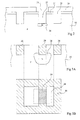
- FIG. 2 represents an initial step in the production of a contact structure on a deep region according to the present invention.
- a protective layer 21, for example 100 nm thick silicon nitride, is deposited on a P-type silicon substrate 10.
- the layer 21 is etched and trenches are created in the upper part of the silicon substrate 10, for example according to the pattern illustrated in the top view of FIG. 1B. Three trench cuts are shown.
- a resin mask 24 creates an opening 25 in line with the central trench 27.
- Arsenic is implanted at a dose of less than 5 ⁇ 10 16 at / cm 2 and with an energy of less than 100 keV through this opening.
- the arsenic ions are then stopped by the resin 24 or the layer 21 so that only the bottom of the central trench 27 is implanted in a silicon region 26.
- Figures 3A and 3B show a next step of the realization of the contact structure on a region deep according to the present invention.
- Figure 3A shows part of the silicon substrate seen in section;
- Figure 3B represents a part of the silicon substrate seen from above.
- a chemical mechanical polishing step and annealing complete the process of creating insulating trenches.
- Below the central trench a intermediate region of type 28 silicon is obtained by diffusion of dopants, implanted in region 26, during said annealing.
- Figure 3B represents two entirely surrounded silicon regions of a trench 29, 30.
- FIG. 4 illustrates a next step in the method of manufacturing the contact structure on a deep region.
- High-dose phosphorus is implanted to form a doped silicon well 40 located between the central trench 29 and the right trench.
- phosphorus is implanted with a dose of between 2x10 15 and 2x10 16 at / cm 2 with an energy of 400 keV.
- Annealing for example of 950 ° C. for twenty minutes, allows the diffusion of this well 40 so that it partially covers the intermediate region 28 in a silicon region 41.
- the silicon well 40 being bounded by trenches , does not extend laterally even in the event of significant thermal diffusion of the dopants.
- High energy phosphorus is then implanted in a deep silicon region 42 located between the central trench 29 and the left trench.
- the trenches mask and laterally limit this settlement.
- phosphorus is implanted with a dose of between 5 ⁇ 10 14 and 2 ⁇ 10 16 16 at / cm 3 with an energy greater than 300 keV. Rapid annealing, for example of 1000 ° C. for 10 s, allows the electrical activation of the implanted phosphorus without causing significant diffusion.
- the deep region 42, of type N covers part of the intermediate region 28 of type N, previously diffused, in a region of silicon 43.
- the region 42 delimits a box of silicon 44 of type P whose borders are the deep region 42, the trenches and the surface of the substrate.
- the well 44 has the type and the level of doping of the initial substrate. It is then, in the case of the present example, entirely isolated from the P-type substrate 10 as well. In fact, the box 44 is isolated vertically by junctions and laterally by the trenches.
- regions 42, 28, 40 of the FIG. 4 are similar respectively to those of regions 7, 2, 5 of Figure 1A.
- the deep region 42 is like the region 7, a transition region for the current. She also has a role of vertical insulation which requires an increase in sound doping.
- the intermediate region 28 has a role similar to that of the buried layer 2: it conducts the current of the region deep 42 towards the doped silicon well 40. However the dimensions of this intermediate region are greatly reduced by compared to those of the buried layer 2. Capacities parasites and the resistances associated with this layer will also very small.
- Figure 4 allows better compromise for the integration of devices requiring buried layer. It is not limited when the dimensions devices decrease. It is all the more effective as the dimensions are small, less than 0.5 ⁇ m and preferably less than 0.1 ⁇ m.
- the process is economical because no epitaxy step, expensive in an industrial environment, has not been used.
- the doping profiles obtained by this process are reproducible because they are obtained from implantations ionic and limited thermal annealing. The yield of manufacturing of integrated circuits is improved.
- FIG. 5 represents the doping profile along the axis vertical AA ′ in FIG. 4.
- This axis AA ′ crosses the box 44 and the deep layer 42 perpendicular to the surface of the silicon.
- the abscissa axis represents the depth (d) at from the surface of substrate 10
- the ordinate axis represents the concentration (c) of doping atoms on a scale logarithmic.
- This doping profile demonstrates the isolation by vertically junctions of the silicon box 44 of P type with respect to P type substrate 10. To obtain this insulation it is necessary to reverse polarize the two N / P junctions created between regions 42 and 44 on the one hand and between the region 42 and the substrate 10 on the other hand. Positive tension must be applied to deep region 42, using the region intermediate 28 and well 40.
- Figure 6 shows the concentration c as a function of the depth d along the vertical axis BB 'of FIG. 4.
- This axis BB ' crosses the doped silicon well 40, the region 41 and region 28.
- This doping profile demonstrates continuity between regions 40 and 28 and in particular the superimposition of the concentrations of the doping atoms of the regions 40 and 28 in the region 41.
- This over-concentration of the region 41 associated with the shallow depth of the doped well 40 allows obtain minimum resistance for current flow successively crossing regions 40 and 28 in the direction of axis BB '.
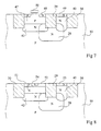
- Figure 7 shows the structure of a transistor Lateral MOS according to the present invention, the box of which is fully insulated. From technological operations performed in Figure 4, an ionic implantation of boron is made in the silicon box 44 now designated by reference 47.
- This layout allows the adjustment of the doping level of the silicon substrate 47 of the future transistor MOS.
- Conventionally we grow a gate oxide, we deposit and etch polycrystalline silicon 50 which forms the gate of the MOS transistor.
- the substrate 47 of this MOS transistor is fully isolated from the initial substrate 10 as long as a positive potential difference exists between deep region 42 and silicon regions adjacent opposite doping.
- This configuration known as name of triple box was obtained without heat treatment important - which is incompatible with the processes of submicronic manufacturing - and without growth of a layer of epitaxial silicon.
- the level of doping of region 42 allows to adjust the voltage withstand of the substrate 47 of the MOS transistor with respect to the initial substrate 10 and to reduce the gain of the parasitic bipolar transistor formed by the substrate 47 of the MOS transistor, deep region 42, and the initial substrate 10.
- the parasitic thyristor generated by sources and drains 48 of the MOS transistor, the insulated box 47, the deep region 42 and the substrate 10 is also an important parameter for optimizing this structure. In particular this thyristor parasite cannot be triggered if the potential of the area deep 42 is well controlled.
- the resistance to access to the deep region 42 across the region intermediate 28 and the doped silicon well 40 is weak.
- the present invention allows easy control of all physical parameters of regions 49, 40, 28, 42, 47 so optimize this triple box structure.
- the compactness of the structure obtained allows easy integration into high integration density digital circuits using MOS transistors. This compactness also makes it possible to reduce all internal parasitic resistances and thus avoid the nuisance triggering of parasitic thyristors.
- Figure 8 shows the structure of a transistor bipolar according to the present invention. From operations shown in Figure 4, an implementation is carried out phosphorus in region 44. This location compensates the initial P-type doping level of this region and allows to locally obtain a region 51 whose doping is of type N. By current operations in bipolar technology we realize then the base 52 of the bipolar transistor, the contact point 53 of the collector and the emitter region 54. The present invention allows to obtain a low resistance between the collector intrinsic 51 of the bipolar transistor and the collector socket 53. The surface between zones 42, 28, 40 on the one hand and on the other apart the substrate 10 is minimized and circumscribed inside of the perimeter defined by the trenches surrounding the transistor bipolar. The capacity of the collector of the bipolar transistor is low. The two features above allow significantly increase the dynamic performance of the component, in particular the maximum operating frequency (Furax) as well as the transition frequency (Ft).
- Furax maximum operating frequency
- Ft transition frequency
- the present invention is capable of various variations and modifications that will appear to humans art.
- any type of substrate can be used. departure as long as there is a weakly layer on its surface doped.
- the epitaxial substrates used in MOS technology are suitable for the present invention. These silicon substrates, very strongly doped in volume, have a layer of epitaxial silicon on their front face 10 to 20 ⁇ m thick and lightly doped.
- any device operating vertically, the current to be collected in volume, can advantageously be made from the present invention.
Landscapes
- Bipolar Transistors (AREA)
Abstract
L'invention concerne la réalisation d'un contact avec une région profonde (42) d'un premier type de conductivité formée dans un substrat (10) en silicium comportant notamment un puits en silicium dopé (40) du premier type de conductivité et une région intermédiaire de connexion entre la couche profonde et le puits. Cette région intermédiaire de connexion est située au-dessous d'une tranchée (29). Le procédé de fabrication permet la réalisation de dispositifs verticaux, en particulier de transistors bipolaires rapides. <IMAGE>
Description
La présente invention concerne le domaine des circuits
intégrés et plus particulièrement la réalisation d'une structure
de contact avec une région profonde et dopée dans un substrat de
silicium.
Certains composants électroniques constituant les
circuits intégrés sont réalisés verticalement. C'est le cas, par
exemple, des transistors bipolaires verticaux. L'émetteur et la
base du transistor bipolaire vertical se situent en surface de
la tranche en silicium. Le collecteur du transistor bipolaire
est en profondeur dans le substrat. On doit alors réaliser la
connexion entre le collecteur en profondeur et les
interconnexions de surface du circuit intégré.
Un exemple de réalisation d'un transistor bipolaire
NPN classique d'un circuit intégré est donné en figure 1A.
Dans un substrat 1 en silicium de type de conductivité
P on implante localement des ions de façon à créer des régions 2
de type de conductivité N. On fait croítre alors une couche
épitaxiée 3 de type de conductivité N au-dessus de toute la
surface du silicium. La région en silicium 2 devient alors une
région enterrée. A titre d'exemple les ions dopant le substrat 1
sont des ions de bore avec une concentration de 1x10¹⁵ at/cm3.
Les ions dopant la région 2 sont des ions d'arsenic avec une
concentration de 5x10¹⁹ at/cm3. Les ions dopant la couche
épitaxiée 3 sont des ions de phosphore avec une concentration de
5x10¹⁵ at/cm3.
Au-dessus de cette région enterrée 2, et à l'intérieur
de la couche 3, on réalise un transistor bipolaire. Ce
transistor bipolaire comporte un puits en silicium 5, un
collecteur intrinsèque 6, une base 8 et un émetteur 9.
Le puits en silicium 5 est une région de silicium, du
même type de conductivité N que la région 2, qui relie la région
enterrée 2 à la surface de la tranche. Le collecteur intrinsèque
6 est une région de silicium du même type de conductivité que la
région enterrée 2 et en contact électrique avec celle-ci grâce à
une région de transition implantée 7 du même type de
conductivité que les régions 6 et 2. La base 8 du transistor
bipolaire est une région de silicium du type de conductivité P
située à la surface du substrat. La base 8 est réalisée à
l'intérieur de la couche épitaxiale 3 et se situe au-dessus du
collecteur intrinsèque 6. L'émetteur 9 est une région de type de
conductivité N, fortement dopée et strictement incluse dans la
base 8. Afin d'isoler latéralement les divers éléments
constitutifs du transistor bipolaire on utilise des tranchées 4
remplies d'oxyde. On entoure ainsi entièrement la base 8 par la
tranchée 4 afin de l'isoler latéralement du puits en silicium 5.
La figure 1B, vue de dessus de la figure 1A,
représente la tranchée 4 entourant entièrement la base 8 et le
puits collecteur 5. Les autres régions de la figure 1A ne sont
pas représentées, pour des raisons de clarté, sur cette figure
1B. Les prises de contacts sur l'émetteur, la base et le
collecteur ne sont pas représentées sur la figure 1B. De même on
n'a pas représenté un éventuel caisson P entourant le transistor
bipolaire afin de l'isoler des autres éléments du circuit
intégré.
Le fonctionnement d'un tel transistor est classique.
Tant que le potentiel entre la base et l'émetteur n'est pas
positif, les électrons situés dans l'émetteur 9 ne peuvent pas
franchir la barrière de potentiel générée par la jonction
base/émetteur. Dès que cette barrière de potentiel s'abaisse un
flux d'électrons s'écoule de l'émetteur vers le collecteur
intrinsèque. Le courant électrique ainsi généré est dirigé vers
la surface du circuit intégré afin d'être traité par les autres
éléments de ce circuit. Le courant collecteur parcourt successivement
la région de transition 7, la couche enterrée 2 et le
puits collecteur 5.
On cherche à optimiser le transistor bipolaire de
façon à obtenir les performances les plus élevées possible. Pour
cela l'homme du métier tente de diminuer l'épaisseur de la base
8 et de réduire toutes les capacités et les résistances internes
du dispositif. Des contraintes dues au procédé technologique
limitent la réduction de l'épaisseur de la base. C'est le cas,
en particulier, lorsque les dopants de la région de transition 7
ou de la région enterrée 2 diffusent vers la surface dans la
base 8. Le niveau de dopage de cette base est alors
incontrôlable. On doit, pour éviter ce phénomène, diminuer les
concentrations de dopants dans la région de transition 7 et dans
la couche enterrée 2. On doit également augmenter la distance de
ces sources de dopant à la base 8. Les résistances internes du
dispositif augmentent alors fortement car les niveaux de dopage
diminuent et les distances à parcourir par le courant
augmentent. La capacité entre le collecteur et le substrat du
transistor bipolaire doit également être optimisée afin
d'améliorer les performances du transistor bipolaire. Cette
capacité est proportionnelle à la surface de la jonction entre
les régions 2 et le substrat 1. Il faut pour améliorer les
performances du transistor bipolaire réduire la taille de la
région 2 sans augmenter aucune résistance interne du dispositif.
Les différents niveaux de dopage et les dimensions
internes du dispositif sont de plus en plus difficiles à
optimiser au fur et à mesure que les règles de dessin qui gèrent
les dimensions minimales utilisables pour le dispositif
diminuent.
Un objet de la présente invention est de permettre la
diminution des résistances internes d'un dispositif utilisant
une région profonde dopée et la diminution de la capacité
parasite de ladite région profonde, c'est-à-dire la réduction
des dimensions de ladite région profonde.
Un autre objet de la présente invention est
d'accroítre les performances des transistors bipolaires
verticaux.
Un autre objet de la présente invention est de
diminuer sensiblement les coûts de fabrication des dispositifs
nécessitant un contact vers une couche profonde de silicium
dopé.
Pour atteindre ces objets, la présente invention
prévoit une structure de contact avec une région profonde d'un
premier type de conductivité formée dans un substrat semiconducteur,
comportant une tranchée adjacente à la région profonde ;
une région intermédiaire du premier type de conductivité située
au-dessous de la tranchée et en contact électrique avec la
région profonde ; et un puits en silicium dopé du premier type
de conductivité en contact électrique avec la région
intermédiaire et disjoint de la région profonde.
Selon un mode de réalisation de la présente invention,
le premier type de conductivité est N ; le substrat est du
silicium monocristallin dont le type de conductivité est P ; le
dopage de la région profonde est supérieur à 5x10¹⁸ at/cm3 ; le
dopage de la région intermédiaire est supérieur à 1x10¹⁹ at/cm3 ;
et le dopage du puits en silicium dopé est supérieur à
1x10¹⁹ at/cm3.
Selon un mode de réalisation de la présente invention,
la région intermédiaire recouvre partiellement la région
profonde et le puits en silicium dopé.
Selon un mode de réalisation de la présente invention,
la région profonde est bornée latéralement, au moins en sa
partie supérieure, par une tranchée.
Selon un mode de réalisation de la présente invention,
la région profonde, la région intermédiaire et le puits dopé
constituent la prise de contact du collecteur d'un transistor
bipolaire.
Selon un mode de réalisation de la présente invention,
la région profonde constitue la base profonde d'un transistor
bipolaire et la région intermédiaire et le puits dopé
constituent la prise de contact sur la base profonde du transistor
bipolaire.
Selon un mode de réalisation de la présente invention,
la région profonde est disposée entre un caisson d'un second
type de conductivité et le substrat d'un second type de
conductivité afin d'isoler le caisson du substrat.
La présente invention prévoit aussi un procédé de
réalisation d'un contact avec une région profonde d'un premier
type de conductivité formée dans un substrat en silicium d'un
second type de conductivité, comportant les étapes suivantes :
Selon un mode de réalisation de la présente invention,
une tranchée remplie d'au moins un matériau diélectrique
délimite l'implantation du dopant du premier type de
conductivité dans la région profonde.
Selon un mode de réalisation de la présente invention,
la région profonde et la tranchée remplie isolent le substrat
initial du substrat d'un second type de conductivité d'un
transistor MOS.
Ces objets, caractéristiques et avantages, ainsi que
d'autres de la présente invention seront exposés en détail dans
la description suivante de modes de réalisation particuliers
faite à titre non-limitatif en relation avec les figures jointes
parmi lesquelles :
Dans les diverses figures, des éléments homologues
sont désignés par les mêmes références. De plus, comme cela est
habituel dans la représentation des circuits intégrés, les
diverses figures ne sont pas tracées à l'échelle.
La figure 2 représente une étape initiale de la réalisation
d'une structure de contact sur une région profonde selon
la présente invention. On dépose sur un substrat en silicium 10
de type P, une couche de protection 21, par exemple du nitrure
de silicium de 100 nm d'épaisseur. En utilisant une étape de
photolithographie on grave la couche 21 et on crée, dans la
partie supérieure du substrat en silicium 10 des tranchées, par
exemple selon le motif illustré dans la vue de dessus de la
figure 1B. Trois coupes de tranchée sont représentées. Un masque
de résine 24 crée une ouverture 25 au droit de la tranchée
centrale 27. On implante de l'arsenic à une dose inférieure à
5x10¹⁶ at/cm2 et avec une énergie inférieure à 100 keV à travers
cette ouverture. Les ions d'arsenic sont alors stoppés par la
résine 24 ou la couche 21 de telle façon que seul le fond de la
tranchée centrale 27 soit implanté dans une région en silicium
26.
Les figures 3A et 3B représentent une étape suivante
de la réalisation de la structure de contact sur une région
profonde selon la présente invention. La figure 3A représente
une partie du substrat de silicium vu en coupe ; la figure 3B
représente une partie du substrat de silicium vu de dessus. On
élimine la résine 24, et on remplit, de manière classique, les
tranchées avec un isolant. Une étape de polissage mécano-chimique
et un recuit terminent le processus de création des
tranchées isolantes. Au-dessous de la tranchée centrale une
région intermédiaire en silicium 28 de type N est obtenue par
diffusion des dopants, implantés dans la région 26, durant ledit
recuit. Pour des raisons de clarté on désigne par la référence
29 les tranchées remplies situées au-dessus d'une région
intermédiaire 28 et par la référence 30 les tranchées remplies
non situées au-dessus d'une région intermédiaire 28. La figure
3B représente deux régions de silicium entièrement entourées
d'une tranchée 29, 30.
La figure 4 illustre une étape suivante du procédé de
fabrication de la structure de contact sur une région profonde.
On implante du phosphore à forte dose pour former un puits de
silicium dopé 40 situé entre la tranchée centrale 29 et la
tranchée de droite. Par exemple on implante du phosphore avec
une dose comprise entre 2x10¹⁵ et 2x10¹⁶ at/cm2 avec une énergie
de 400 keV. Un recuit, par exemple de 950°C pendant vingt
minutes, permet la diffusion de ce puits 40 de façon à ce qu'il
recouvre partiellement la région intermédiaire 28 dans une
région en silicium 41. Le puits en silicium 40 étant borné par
des tranchées, ne s'étend pas latéralement même en cas de
diffusion thermique importante des dopants. On implante ensuite
du phosphore à forte énergie dans une région profonde en
silicium 42 située entre la tranchée centrale 29 et la tranchée
de gauche. Les tranchées masquent et bornent latéralement cette
implantation. Par exemple on implante du phosphore avec une dose
comprise entre 5x10¹⁴ et 2x10¹⁶ at/cm3 avec une énergie supérieure
à 300 keV. Un recuit rapide, par exemple de 1000°C pendant 10 s,
permet l'activation électrique du phosphore implanté sans
provoquer de diffusion importante. La région profonde 42, de
type N, recouvre une partie de la région intermédiaire 28 de
type N, précédemment diffusée, dans une région en silicium 43.
La région 42 délimite un caisson en silicium 44 de type P dont
les frontières sont la région profonde 42, les tranchées et la
surface du substrat. Une implantation ionique optionnelle
effectuée dans ce caisson permet d'ajuster le type et le niveau
de dopage du caisson 44. Si aucune implantation n'est effectuée,
le caisson 44 possède le type et le niveau de dopage du substrat
initial. Il est alors, dans le cas du présent exemple,
entièrement isolé du substrat 10 de type P également. En effet
le caisson 44 est isolé verticalement par des jonctions et
latéralement par les tranchées.
Ainsi on vient de créer une structure de contact avec
une région profonde 42 de type N constituée d'une région
intermédiaire 28 et d'un puits en silicium dopé 40. On assure un
contact électrique de faible résistance entre les différentes
régions de cette structure par le recouvrement des régions 28 et
40 dans la zone 41 et des régions 28 et 42 dans la zone 43.
Les fonctionnalités des régions 42, 28, 40 de la
figure 4 sont similaires respectivement à celles des régions 7,
2, 5 de la figure 1A. La région profonde 42 est comme la région
7, une région de transition pour le courant. Elle a en plus un
rôle d'isolation verticale qui nécessite une augmentation de son
dopage. La région intermédiaire 28 a un rôle similaire à celui
de la couche enterrée 2 : elle conduit le courant de la région
profonde 42 vers le puits de silicium dopé 40. Cependant les
dimensions de cette région intermédiaire sont très réduites par
rapport à celles de la couche enterrée 2. Les capacités
parasites et les résistances associées à cette couche seront
également très réduites.
La structure de la figure 4 autorise de meilleurs
compromis pour l'intégration des dispositifs nécessitant une
couche enterrée. Elle n'est pas limitée lorsque les dimensions
des dispositifs diminuent. Elle est d'autant plus efficace que
les dimensions sont petites, inférieures à 0.5 µm et de
préférence inférieures à 0.1 µm.
Le procédé est économique car aucune étape d'épitaxie,
coûteuse en milieu industriel, n'a été utilisée.
Les profils de dopage obtenus par ce procédé sont
reproductibles car ils sont obtenus à partir d'implantations
ioniques et de recuits thermiques limités. Le rendement de
fabrication des circuits intégrés est amélioré.
La figure 5 représente le profil de dopage selon l'axe
vertical AA' de la figure 4. Cet axe AA' traverse le caisson 44
et la couche profonde 42 perpendiculairement à la surface du
silicium. L'axe des abscisses représente la profondeur (d) à
partir de la surface du substrat 10, l'axe des ordonnées représente
la concentration (c) d'atomes dopants suivant une échelle
logarithmique. Ce profil de dopage démontre l'isolation par
jonctions, dans le sens vertical, du caisson en silicium 44 de
type P vis à vis du substrat 10 de type P. Pour obtenir cette
isolation il faut polariser en inverse les deux jonctions N/P
créées entre les régions 42 et 44 d'une part et entre la région
42 et le substrat 10 d'autre part. Une tension positive doit
être appliquée à la région profonde 42, en utilisant la région
intermédiaire 28 et le puits 40.
La figure 6 représente la concentration c en fonction
de la profondeur d selon l'axe vertical BB' de la figure 4. Cet
axe BB' traverse le puits en silicium dopé 40, la région 41 et
la région 28. Ce profil de dopage démontre la continuité
électrique entre les régions 40 et 28 et en particulier la
superposition des concentrations des atomes dopants des régions
40 et 28 dans la région 41. Cette sur-concentration de la région
41 associée à la faible profondeur du puits dopé 40 permet
d'obtenir une résistance minimale pour le flux de courant
traversant successivement les régions 40 et 28 dans le sens de
l'axe BB'.
La figure 7 représente la structure d'un transistor
MOS latéral selon la présente invention dont le caisson est
entièrement isolé. A partir des opérations technologiques
réalisées à la figure 4, une implantation ionique de bore est
effectuée dans le caisson en silicium 44 désigné maintenant par
la référence 47. Cette implantation permet l'ajustement du
niveau de dopage du substrat en silicium 47 du futur transistor
MOS. De manière classique on fait croítre un oxyde de grille, on
dépose et on grave du silicium polycristallin 50 qui forme la
grille du transistor MOS. On implante avec une forte dose
d'arsenic les régions 48 de source et drain du transistor MOS
ainsi que la surface 49 du puits en silicium dopé 40. Le
substrat 47 de ce transistor MOS est entièrement isolé du
substrat initial 10 tant qu'une différence de potentiel positive
existe entre la région profonde 42 et les régions en silicium
adjacentes de dopage opposé. Cette configuration connue sous le
nom de triple caisson à été obtenue sans traitement thermique
important - ce qui est incompatible avec les procédés de
fabrication submicronique - et sans croissance d'une couche de
silicium épitaxiée. Le niveau de dopage de la région 42 permet
d'ajuster la tenue en tension du substrat 47 du transistor MOS
vis à vis du substrat initial 10 et de réduire le gain du
transistor bipolaire parasite formé par le substrat 47 du
transistor MOS, la région profonde 42, et le substrat initial
10. Le thyristor parasite généré par les sources et les drains
48 du transistor MOS, le caisson isolé 47, la région profonde 42
et le substrat 10 est également un paramètre important pour
l'optimisation de cette structure. En particulier ce thyristor
parasite ne peut pas se déclencher si le potentiel de la région
profonde 42 est bien contrôlé. Pour cela il faut que la
résistance d'accès à la région profonde 42 à travers la région
intermédiaire 28 et le puits en silicium dopé 40 soit faible. La
présente invention permet un contrôle aisé de tous les
paramètres physiques des régions 49, 40, 28, 42, 47 afin
d'optimiser cette structure à triple caisson. La compacité de la
structure obtenue permet une intégration facile dans les
circuits numériques à haute densité d'intégration utilisant des
transistors MOS. Cette compacité permet également de diminuer
toutes les résistances internes parasites et d'éviter ainsi le
déclenchement intempestif des thyristors parasites.
La figure 8 représente la structure d'un transistor
bipolaire selon la présente invention. A partir des opérations
technologiques réalisées à la figure 4, on réalise une implantation
de phosphore dans la région 44. Cette implantation compense
le niveau de dopage initial de type P de cette région et permet
d'obtenir localement une région 51 dont le dopage est de type N.
Par des opérations courantes en technologie bipolaire on réalise
alors la base 52 du transistor bipolaire, la prise de contact 53
du collecteur et la région 54 d'émetteur. La présente invention
permet d'obtenir une faible résistance entre le collecteur
intrinsèque 51 du transistor bipolaire et la prise collecteur
53. La surface entre d'une part les zones 42, 28, 40 et d'autre
part le substrat 10 est minimisée et circonscrite à l'intérieur
du périmètre défini par les tranchées entourant le transistor
bipolaire. La capacité du collecteur du transistor bipolaire est
faible. Les deux caractéristiques ci-dessus permettent
d'accroítre sensiblement les performances dynamiques du composant,
en particulier la fréquence maximale de fonctionnement
(Furax) ainsi que la fréquence de transition (Ft).
Bien entendu, la présente invention est susceptible de
diverses variantes et modifications qui apparaítront à l'homme
de l'art. En particulier, on peut changer, selon les objectifs,
le type de dopant des différentes couches ainsi que les ions
implantés pour créer les zones dopées.
On peut utiliser n'importe quel type de substrat de
départ tant qu'il existe à sa surface une couche faiblement
dopée. En particulier les substrats épitaxiés utilisés en
technologie MOS sont adaptés à la présente invention. Ces
substrats en silicium, très fortement dopés en volume,
présentent sur leur face avant une couche de silicium épitaxié
de 10 à 20 µm d'épaisseur et faiblement dopé.
On peut utiliser le mode d'accès à des couches
profondes selon la présente invention pour réaliser des accès à
des couches profondes de divers types constituant des éléments
de divers composants.
On peut par exemple réaliser des dispositifs de type
bipolaire avec une base 42 profonde et avec une reprise du
contact de base en surface. On peut agencer ces transistors
bipolaires pour faire des structures thyristor.
Tout dispositif fonctionnant verticalement, le courant
devant être collecté en volume, peut avantageusement être
réalisé à partir de la présente invention.
Claims (9)
- Structure de contact avec une région profonde (42) d'un premier type de conductivité formée dans un substrat semiconducteur, caractérisée en ce qu'elle comporte :une tranchée (29) adjacente à la région profonde (42) ;une région intermédiaire (28) du premier type de conductivité située sous la tranchée (29), sensiblement en alignement avec celle-ci, et en contact électrique avec la région profonde (42) ;un puits en silicium dopé (40) du premier type de conductivité en contact électrique avec la région intermédiaire (28) et disjoint de la région profonde (42).
- Structure de contact selon la revendication 1, caractérisée en ce que :le premier type de conductivité est N ;le substrat est du silicium monocristallin dont le type de conductivité est P ;le dopage de la région profonde (42) est supérieur à 5x10¹⁸ at/cm3 ;le dopage de la région intermédiaire (28) est supérieur à 1x10¹⁹ at/cm3 ;le dopage du puits en silicium dopé (40) est supérieur à 1x10¹⁹ at/cm3.
- Structure de contact selon la revendication 1, caractérisée en ce que la région intermédiaire (28) recouvre partiellement la région profonde (42) et le puits en silicium dopé (40).
- Structure de contact selon la revendication 1, caractérisée en ce que la région profonde (42) est bornée latéralement, au moins en sa partie supérieure, par une tranchée (29, 30).
- Structure de contact selon la revendication 1, caractérisée en ce que la région profonde (42), la région intermédiaire (28) et le puits dopé (40) constituent la prise de contact du collecteur d'un transistor bipolaire.
- Structure de contact selon la revendication 1, caractérisée en ce que la région profonde (42) constitue la base profonde d'un transistor bipolaire et en ce que la région intermédiaire (28) et le puits dopé (40) constituent la prise de contact sur la base profonde du transistor bipolaire.
- Structure de contact selon la revendication 1, caractérisée en ce que la région profonde (42) est disposée entre un caisson (44, 47) d'un second type de conductivité et le substrat (10) d'un second type de conductivité afin d'isoler le caisson (44, 47) du substrat (10).
- Procédé de réalisation d'un contact avec une région profonde (42) d'un premier type de conductivité formée dans un substrat (10) en silicium d'un second type de conductivité, caractérisé en ce qu'il comporte les étapes suivantes :a) graver une tranchée dans le substrat (10) ;b) implanter au fond de la tranchée un dopant qui, après diffusion, formera une région intermédiaire (28) du premier type de conductivité ;c) remplir la tranchée (29) avec au moins un matériau diélectrique ;d) implanter un puits en silicium du premier type de conductivité (40) adjacent à la tranchée (29) ;e) implanter avec un dopant du premier type de conductivité une région profonde (42) adjacente à ladite tranchée (29) et disjointe du puits en silicium dopé (40) ; etf) effectuer au moins un recuit de la structure après l'une au moins des opérations b) à e) de façon à former, par diffusion des dopants implantés sous la tranchée (27, 29), une région intermédiaire (28) du premier type de conductivité se confondant en partie avec la région profonde (42) et le puits (40).
- Procédé selon la revendication 8, caractérisé en ce qu'une tranchée remplie d'au moins un matériau diélectrique (29, 30) délimite l'implantation du dopant du premier type de conductivité dans la région profonde (42).
Applications Claiming Priority (2)
| Application Number | Priority Date | Filing Date | Title |
|---|---|---|---|
| FR0111556A FR2829288A1 (fr) | 2001-09-06 | 2001-09-06 | Structure de contact sur une region profonde formee dans un substrat semiconducteur |
| FR0111556 | 2001-09-06 |
Publications (1)
| Publication Number | Publication Date |
|---|---|
| EP1291922A1 true EP1291922A1 (fr) | 2003-03-12 |
Family
ID=8867040
Family Applications (1)
| Application Number | Title | Priority Date | Filing Date |
|---|---|---|---|
| EP02354133A Pending EP1291922A1 (fr) | 2001-09-06 | 2002-09-04 | Structure de contact sur une région profonde formée dans un substrat semiconducteur |
Country Status (3)
| Country | Link |
|---|---|
| US (1) | US6847094B2 (fr) |
| EP (1) | EP1291922A1 (fr) |
| FR (1) | FR2829288A1 (fr) |
Cited By (1)
| Publication number | Priority date | Publication date | Assignee | Title |
|---|---|---|---|---|
| EP1702349A4 (fr) * | 2003-12-31 | 2010-09-15 | Freescale Semiconductor Inc | Procede pour fabriquer un composant a semi-conducteurs, composant a semi-conducteurs forme selon le procede |
Families Citing this family (3)
| Publication number | Priority date | Publication date | Assignee | Title |
|---|---|---|---|---|
| US6812486B1 (en) * | 2003-02-20 | 2004-11-02 | National Semiconductor Corporation | Conductive structure and method of forming the structure |
| US6815714B1 (en) * | 2003-02-20 | 2004-11-09 | National Semiconductor Corporation | Conductive structure in a semiconductor material |
| US7994536B2 (en) * | 2008-02-19 | 2011-08-09 | Qimonda Ag | Integrated circuit including U-shaped access device |
Citations (3)
| Publication number | Priority date | Publication date | Assignee | Title |
|---|---|---|---|---|
| EP0004292A2 (fr) * | 1978-03-27 | 1979-10-03 | International Business Machines Corporation | Procédé de fabrication d'un transistor bipolaire de type MESA présentant des régions d'émetteur et de base auto-alignées |
| US6184102B1 (en) * | 1996-12-10 | 2001-02-06 | Sgs-Thomson Microelectronics S.A. | Method for manufacturing a well isolation bipolar transistor |
| US6265275B1 (en) * | 1998-06-05 | 2001-07-24 | Stmicroelectronics S.A. | Method of selectively doping the intrinsic collector of a vertical bipolar transistor with epitaxial base |
Family Cites Families (13)
| Publication number | Priority date | Publication date | Assignee | Title |
|---|---|---|---|---|
| JPS5226182A (en) * | 1975-08-25 | 1977-02-26 | Hitachi Ltd | Manufacturing method of semi-conductor unit |
| US4392149A (en) * | 1980-03-03 | 1983-07-05 | International Business Machines Corporation | Bipolar transistor |
| JPS61164262A (ja) * | 1985-01-17 | 1986-07-24 | Toshiba Corp | 半導体装置 |
| US4851362A (en) * | 1987-08-25 | 1989-07-25 | Oki Electric Industry Co., Ltd. | Method for manufacturing a semiconductor device |
| US5006476A (en) * | 1988-09-07 | 1991-04-09 | North American Philips Corp., Signetics Division | Transistor manufacturing process using three-step base doping |
| US5124775A (en) * | 1990-07-23 | 1992-06-23 | National Semiconductor Corporation | Semiconductor device with oxide sidewall |
| JPH04105325A (ja) * | 1990-08-24 | 1992-04-07 | Hitachi Ltd | 半導体集積回路装置 |
| JPH04209540A (ja) * | 1990-12-04 | 1992-07-30 | Takehide Shirato | バイポーラトランジスタ |
| US5187109A (en) * | 1991-07-19 | 1993-02-16 | International Business Machines Corporation | Lateral bipolar transistor and method of making the same |
| JPH07106412A (ja) * | 1993-10-07 | 1995-04-21 | Toshiba Corp | 半導体装置およびその製造方法 |
| JP2679639B2 (ja) * | 1994-09-12 | 1997-11-19 | 日本電気株式会社 | 半導体装置及びその製造方法 |
| US5869881A (en) * | 1994-12-20 | 1999-02-09 | Electronics And Telecommunications Research Institute | Pillar bipolar transistor |
| EP0818829A1 (fr) * | 1996-07-12 | 1998-01-14 | Hitachi, Ltd. | Transistor bipolaire et son procédé de fabrication |
-
2001
- 2001-09-06 FR FR0111556A patent/FR2829288A1/fr active Pending
-
2002
- 2002-09-04 EP EP02354133A patent/EP1291922A1/fr active Pending
- 2002-09-06 US US10/236,082 patent/US6847094B2/en not_active Expired - Lifetime
Patent Citations (3)
| Publication number | Priority date | Publication date | Assignee | Title |
|---|---|---|---|---|
| EP0004292A2 (fr) * | 1978-03-27 | 1979-10-03 | International Business Machines Corporation | Procédé de fabrication d'un transistor bipolaire de type MESA présentant des régions d'émetteur et de base auto-alignées |
| US6184102B1 (en) * | 1996-12-10 | 2001-02-06 | Sgs-Thomson Microelectronics S.A. | Method for manufacturing a well isolation bipolar transistor |
| US6265275B1 (en) * | 1998-06-05 | 2001-07-24 | Stmicroelectronics S.A. | Method of selectively doping the intrinsic collector of a vertical bipolar transistor with epitaxial base |
Cited By (1)
| Publication number | Priority date | Publication date | Assignee | Title |
|---|---|---|---|---|
| EP1702349A4 (fr) * | 2003-12-31 | 2010-09-15 | Freescale Semiconductor Inc | Procede pour fabriquer un composant a semi-conducteurs, composant a semi-conducteurs forme selon le procede |
Also Published As
| Publication number | Publication date |
|---|---|
| US6847094B2 (en) | 2005-01-25 |
| FR2829288A1 (fr) | 2003-03-07 |
| US20030042574A1 (en) | 2003-03-06 |
Similar Documents
| Publication | Publication Date | Title |
|---|---|---|
| EP0057126B1 (fr) | Procédé de fabrication d'une structure de transistors | |
| FR2652448A1 (fr) | Procede de fabrication d'un circuit integre mis haute tension. | |
| WO1996032738A1 (fr) | PROCEDE D'INTRODUCTION D'UNE IMPURETE AGISSANT COMME DOPANT DANS LE SiC, DISPOSITIF SEMI-CONDUCTEUR ELABORE SELON CE PROCEDE ET UTILISATION D'UNE COUCHE AMORPHE FORTEMENT DOPEE COMME SOURCE DE DIFFUSION DE DOPANT DANS LE SiC | |
| EP0462882A1 (fr) | Transistor à effet de champ en couche mince avec grille enterrée et son procédé de fabrication | |
| FR2530867A1 (fr) | Dispositifs mos a barriere de schottky et leur procede de fabrication | |
| FR2649831A1 (fr) | Dispositif soi-mos presentant une structure de paroi laterale conductrice et procede pour sa fabrication | |
| TW201924060A (zh) | 具有減小的橫向電場之電晶體元件 | |
| FR2953062A1 (fr) | Diode de protection bidirectionnelle basse tension | |
| US20050215024A1 (en) | Methods for forming super-steep diffusion region profiles in MOS devices and resulting semiconductor topographies | |
| US5147809A (en) | Method of producing a bipolar transistor with a laterally graded emitter (LGE) employing a refill method of polycrystalline silicon | |
| US8476143B2 (en) | Deep contacts of integrated electronic devices based on regions implanted through trenches | |
| EP1146561A1 (fr) | Procédé de réalisation d'un transistor bipolaire | |
| EP1291922A1 (fr) | Structure de contact sur une région profonde formée dans un substrat semiconducteur | |
| FR2482368A1 (fr) | Operateur logique a injection par le substrat et son procede de fabrication | |
| FR2742583A1 (fr) | Transistor a effet de champ a grille isolee et a canal diffuse | |
| KR20000062635A (ko) | 상보형 금속 산화 반도체 장치용 2중 게이트 구조 제조 방법 | |
| JP3361842B2 (ja) | 半導体素子、システム及び方法 | |
| US6599817B1 (en) | Semiconductor constructions, and methods of forming semiconductor constructions | |
| FR3078197A1 (fr) | Dispositif de transistor bipolaire et procede de fabrication correspondant | |
| EP0037764B1 (fr) | Structure de dispositif à semiconducteur à anneau de garde, et à fonctionnement unipolaire | |
| EP0948038B1 (fr) | Procédé de fabrication d'une diode à avalanche à seuil réglable | |
| EP1146554A1 (fr) | Procédé de formation de couches enterrées | |
| US7479438B2 (en) | Method to improve performance of a bipolar device using an amorphizing implant | |
| JP3216287B2 (ja) | 半導体装置 | |
| JPH0239534A (ja) | 半導体装置の製造方法 |
Legal Events
| Date | Code | Title | Description |
|---|---|---|---|
| PUAI | Public reference made under article 153(3) epc to a published international application that has entered the european phase |
Free format text: ORIGINAL CODE: 0009012 |
|
| AK | Designated contracting states |
Kind code of ref document: A1 Designated state(s): AT BE BG CH CY CZ DE DK EE ES FI FR GB GR IE IT LI LU MC NL PT SE SK TR Designated state(s): AT BE BG CH CY CZ DE DK EE ES FI FR GB GR IE IT LI LU MC NL PT SE SK TR |
|
| AX | Request for extension of the european patent |
Extension state: AL LT LV MK RO SI |
|
| 17P | Request for examination filed |
Effective date: 20030905 |
|
| AKX | Designation fees paid |
Designated state(s): DE FR GB IT |
|
| STAA | Information on the status of an ep patent application or granted ep patent |
Free format text: STATUS: THE APPLICATION IS DEEMED TO BE WITHDRAWN |