EP1300908A1 - Filter - Google Patents
Filter Download PDFInfo
- Publication number
- EP1300908A1 EP1300908A1 EP01947893A EP01947893A EP1300908A1 EP 1300908 A1 EP1300908 A1 EP 1300908A1 EP 01947893 A EP01947893 A EP 01947893A EP 01947893 A EP01947893 A EP 01947893A EP 1300908 A1 EP1300908 A1 EP 1300908A1
- Authority
- EP
- European Patent Office
- Prior art keywords
- filter
- slit
- conductor
- waveguide tube
- tube structure
- Prior art date
- Legal status (The legal status is an assumption and is not a legal conclusion. Google has not performed a legal analysis and makes no representation as to the accuracy of the status listed.)
- Withdrawn
Links
Images




Classifications
-
- H—ELECTRICITY
- H01—ELECTRIC ELEMENTS
- H01P—WAVEGUIDES; RESONATORS, LINES, OR OTHER DEVICES OF THE WAVEGUIDE TYPE
- H01P1/00—Auxiliary devices
- H01P1/20—Frequency-selective devices, e.g. filters
- H01P1/207—Hollow waveguide filters
- H01P1/208—Cascaded cavities; Cascaded resonators inside a hollow waveguide structure
- H01P1/2088—Integrated in a substrate
Definitions
- the present invention relates to a filter having a waveguide tube structure for use as a high-frequency component.
- Typical waveguide tube filters used in microwave and millimeter-wave bands are realized by using a resonator structure including a metallic waveguide tube formed in a drawn structure. This type of the filters has a drawback in larger dimensions although it is superior in the performance thereof.
- a pseudo waveguide tube band-pass filter which has a side wall of the waveguide tube configured by metallic via-holes in a dielectric substrate.
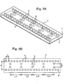
- Figs. 9A and 9B show the schematic structure of a filter having a four-stage configuration.
- Fig. 9A is a perspective view thereof
- Fig. 9B is a top plan view thereof.
- a top conductor 2 is formed on one of the surfaces of the dielectric substrate 1
- a bottom conductor 3 is formed on the opposing surface thereof.
- Via-holes 4 connecting together the top conductor 2 and the bottom conductor 3 are formed in two rows along the signal transfer direction.
- the spacing "a" between adjacent via-holes is equal to or below 1/2 of the in-tube wavelength.
- This structure is construed as a pseudo waveguide tube having a waveguide tube cross section defined by the thickness of the dielectric and the spacing "b" between the two rows of the via-holes 5 arranged. Pairs of via-holes 5 are also formed in the waveguide tube to configure resonators having cavity lengths of L1, L2, L3 and L4.
- the spacing "c" between the via-holes 5 forming a pair frequencies other than the resonant frequency can be effectively reflected.
- a signal in the resonant frequency passes therethrough to achieve a desired filter function. In this filter, the dimensions of the filter are reduced down to about 1/ ⁇ compared to a waveguide tube having a hollow interior ( ⁇ is the relative permittivity of the dielectric).
- a filter is often used which is configured by using a micro-strip line on a dielectric substrate.
- This filter has relatively smaller dimensions and can be connected to a planar circuit, such as an integrated circuit, by wire bonding, thereby allowing the filter to be mounted in a high-frequency module with ease.
- the above waveguide tube filer is sometimes requested to have smaller dimensions.
- the dimensions of the microwave or millimeter-wave integrated circuit formed on a semiconductor device are of around 5mm square at a maximum. Accordingly, if a small-size multi-chip module is to be implemented by using an integrated circuit, it is generally important to reduce the dimensions of passive components such as a filter. In addition, it is generally difficult to connect the filter to a planar circuit. Thus, a filter is desired which can be mounted and connected with ease and without enlarging the dimensions and adding a particular conversion circuit.
- the filter using the micro-strip line sometimes assumes a characteristic change upon mounting the filter in a package structure. This results from the fact that the electromagnetic field in the micro-strip line is distributed up to the top portion thereof and thus liable to the influence by attaching a cap member thereto.
- connection structure using the wire bonding technique especially in the higher frequency range such as millimeter wave band, there arises a characteristic change caused by variation of the wire length or by variation of the parasitic inductance component determined by the wire length.
- a characteristic change is not negligible, and becomes a factor of reducing the product yield in a mass production.
- a flip-chip mounting technique has been developed wherein the millimeter-wave semiconductor integrated circuit is mounted with face-down mounting onto a mounting board and connected thereto by using bumps. This technique is described in a literature, "IEEE International Solid-State Circuits Symposium, Digest" pp.324-325, 2000, by K.Maruhashi et al., for example.
- the connection between each element and the mounting board is implemented by a relatively short distance (200 micrometers or less), whereby the influence by the parasitic inductance component and variation thereof which is generally a matter of problem in the wire bonding technique becomes negligible.
- the filter should have a terminal adapted to a coplanar waveguide, which is generally used for connection between elements, and should have a structure wherein the face-down mounting scarcely changes the filter characteristic, and thus such a filter has been strongly desired.
- the present invention provides, in a first aspect thereof, a filter including a rectangular waveguide tube structure filled with dielectric, wherein the rectangular waveguide structure configures therein at least one resonator, characterized in that:
- the present invention provides, in a second aspect thereof, a filter including a rectangular waveguide tube structure including a pair of first conductor planes formed on top and bottom surfaces of a dielectric substrate, and a pair of second conductor planes formed on side surfaces of the dielectric substrate, wherein the first conductor planes constitute longer-side conductor planes, and the rectangular waveguide tube structure configures therein at least one resonator, characterized in that:
- the present invention provides, in a third aspect thereof, a filter including a rectangular waveguide tube structure including a pair of conductor planes formed on top and bottom surfaces of a dielectric substrate, conductor via-holes formed in the dielectric substrate, wherein the conductor planes constitute longer-side conductor planes, and the rectangular waveguide tube structure configures at least one resonator, characterized in that:
- the slit be formed in a portion of the longer-side conductor plane of the waveguide tube structure configuring a central resonator among an add number of resonators arranged.
- the slit extend in a direction perpendicular to the signal transfer direction.
- the conductor plane configuring the waveguide tube structure mount thereon a coplanar waveguide, and the coplanar waveguide be connected to the slit.
- the coplanar waveguide and a circuit board for mounting thereon the filter are connected together via a bump.
- the conductor plane configuring the waveguide tube structure mounts thereon a slot line, and the slot line be connected to the slit.
- the slot line and a circuit board mounting thereon the filter be connected together via a bump.
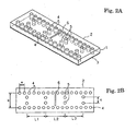
- FIG. 2A and 2B there is shown the schematic structure of a filter according to a first embodiment of the present invention.
- a dielectric substrate 1 is provided with a top conductor 2 formed on a surface thereof, and a bottom conductor 3 formed on the opposing surface thereof.
- Via-holes 4 connecting together the top conductor 2 and the bottom conductor 3 are formed in two rows along a signal transfer direction.
- the spacing "a" between adjacent via-holes is preferably equal to or below 1/2 of the in-tube wavelength.
- This structure can be construed as a pseudo waveguide tube having a waveguide-tube cross section defined by the thickness of the dielectric substrate (in a shorter side) and the spacing between the two rows of the via-holes arranged (in a longer side).
- pairs of via-holes 5 are further formed, thereby configuring resonators having cavity lengths of L1, L2 and L3.
- the spacing "c" between the via-holes 5 forming a pair frequencies other than a resonant frequency can be reflected.
- a signal in the resonant frequency passes therethrough to achieve a desired filter property.
- the present filter has a three-stage structure including three resonators therein, wherein a portion of the top conductor 2 overlying the central resonator is provided with a slit 6 formed by partially removing the conductor.
- the slit 6 is preferably arranged to extend in a direction perpendicular to the signal transfer direction.
- Fig. 3 shows the filter characteristic (insertion loss) in the present embodiment.
- the characteristics of the frequency dependency of the insertion loss of conventional filters are also exemplified, which include a filter having four stages similarly to the filter shown in Fig. 4 and a filter having three stages (not specifically shown in the drawings), both having a 3-dB pass band similar to the 3-dB pass band of the present embodiment.
- the insertion loss in the present embodiment is 40dB at a frequency (55GHz) which is 6GHz apart from the central frequency, 61GHz, toward a lower frequency side. This value is higher than the insertion loss, 25dB, of the conventional three-stage filter and is approximately equal to the value, 42dB, of the conventional four-stage filter.
- the filter has smaller dimensions, whereby lower costs for the filter itself or smaller dimensions of a high-frequency circuit module having such a filter can be achieved.
- the operational principle of the present embodiment is that the introduction of the slit 6 provides an attenuation pole in the lower frequency range to thereby raise the suppression amount of the undesired-frequency-band signal.
- the attenuation pole is formed in the lower frequency range; however, the attenuation pole may be formed in the higher frequency range by adjusting the slit length. It is found that the frequency at which the attenuation pole appears is easily adjusted, without changing the other structural parameters, by changing the slit length for the slit provided above the central resonator among an odd number of the resonators provided in the filter.
- the slit may extend between the via-holes 4, if desired, and can be extended beyond the waveguide tube structure by increasing the length thereof, and accordingly, a higher design choice can be obtained.
- attenuation poles can be provided on both the higher frequency side and the lower frequency side.
- the signal electromagnetic field leaks from the internal of the pseudo waveguide tube through the slit, the influence by the signal electromagnetic field is lower due to the dielectric residing within the pseudo waveguide tube. Accordingly, if it is incorporated in a module, for example, and covered by a cap, the influence to the filter characteristic is lower.
- the filter of the present embodiment can be easily manufactured by using a well-known alumina-ceramic-substrate process etc. More specifically, the filter may be manufactured, while using a ceramic-material sheet, by the steps of forming via-holes, filling therein with metallic paste, baking, forming an interconnection film (forming slit), plating with gold etc. It is to be noted that the material for the substrate, the process for forming the via-holes and the process for forming the slit are not limited in the present invention. In addition, although the via-holes 4 are exemplarily formed in two rows along the signal transfer direction, any number of rows may be employed so long as the pseudo waveguide tube is configured thereby.
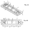
- FIG. 4A and 4B there is shown the schematic structure of a filter according to a second embodiment of the present invention.
- a dielectric substrate is provided with a top conductor 2 formed on one surface thereof, and a bottom conductor 3 formed on the opposite surface thereof.
- Via-holes 4 connecting the top conductor 2 and the bottom conductor 3 together are formed in two rows along the signal transfer direction. It is preferable that the spacing "a" between adjacent via-holes be equal to or less than 1/2 of the in-tube wavelength.
- This structure can be construed as a pseudo waveguide tube having a waveguide-tube cross section defined by the thickness of the dielectric and the spacing "b" between the two rows of the via-holes arranged.
- pairs of via-holes 5 are formed in the waveguide tube to thereby configure resonators having cavity lengths of L1, L2, L3 and L4.
- frequencies other than the resonant frequency can be reflected.
- a signal in the resonant frequency passes therethrough to thereby obtain a desired filter performance.
- the present filter has a four-stage structure including four resonators therein, wherein each of portions of the top conductor 2 overlying the outermost end resonators is provided with slits 7 and 8 formed by partially removing the conductor.
- a coplanar waveguide 9 formed on the top conductor 2 overlying the resonator is connected to the slit 7.
- the coplanar waveguide 9 formed overlying the resonator constitutes a terminal for external connection. Accordingly, it can be manufactured with reduced dimensions compared to the conventional technique (Fig. 9) which necessitates another terminal in the signal transfer direction. In addition, it can be connected to a planar circuit by using a bonding wire technique without using an additional particular conversion section. It is to be noted that although the signal electromagnetic field leaks from the internal of the pseudo waveguide tube through the slit, the influence thereby is lower due to the dielectric residing within the pseudo waveguide tube. Accordingly, if it is incorporated in a module, fore example, and covered by a cap, the influence to the filter characteristic is lower.
- Fig. 5 shows the mounting technique used for the filter according to the present embodiment.
- a coplanar waveguide 13 is formed using a conductor pattern 12 on the mounting board 11, on which the filter 10 of the present embodiment is to be mounted.
- bumps 14 including gold as a main component thereof are formed on the mounting board 11.
- the filter is mounted on and connected to the mounting board 11 via bumps.
- an integrated circuit etc. may be sometimes mounted other than the recited filter.
- the species or fabrication method of the bums are not particularly defined, and thus solder bumps can be used, and the bumps may be formed on the filter side without any problem.
- the mounting board affects the electromagnetic field leaking through the slit, the influence thereby is relatively lower due to the dielectric residing within the pseudo waveguide tube.
- a characteristic change between before and after the mounting process can be suppressed, whereby advantages of the flip-chip mounting technique can be obtained substantially without problems of the parasitic inductance component and variation thereof, which are generally involved in the wire bonding process.
- FIG. 7A and 7B there is shown the schematic structure of a filter according to a third embodiment of the present invention.
- the present filter has a main structure similar to that of the filter shown in Fig. 4, wherein a slot line 16 is connected to the slit 7 while overstriding the slit 8.
- Fig. 8 shows an example of the mounting process of the filter according to the present embodiment.
- a coplanar waveguide 13 using a conductor pattern 12 is formed on the mounting board 11 on which the filter 10 according to the present embodiment is to be mounted.
- a slot line/coplanar waveguide conversion section 18 is formed on the tip of the coplanar waveguide.
- bumps 14 including gold as a main component thereof are formed on the mounting board 11.
- the filter is mounted on the mounting board 11 via bumps 14 by using a heat-press technique, for example.
- the slot line formed on the filter is connected to the coplanar waveguide on the mounting board via the slot line/coplanar waveguide conversion section 18 with an electromagnetic field coupling.
- FIG. 1A and 1B there is shown the schematic structure of a filter according to a fourth embodiment of the present invention.
- a dielectric substrate 1 is provided with a top conductor 2 formed on one surface thereof, and a bottom conductor 3 formed on the opposite surface thereof.
- Via-holes 4 connecting together the top conductor 2 and the bottom conductor 3 are formed in two rows along the signal transfer direction.
- the spacing "a" between adjacent via-holes is preferably equal to or smaller than 1/2 of the in-tube wavelength.
- This structure is construed as a pseudo waveguide tube having a waveguide-tube cross section defined by the thickness of the dielectric and the spacing "b" between two rows of the via-holes arranged.
- pairs of via-holes 5 are formed in the waveguide tube to configure resonators having cavity lengths of L1, L2 and L3.
- frequencies other than the resonant frequency can be reflected.
- a signal in the resonant frequency passes therethrough to thereby obtain a desired filter property.
- the present filter has a three-stage structure including three resonators therein, wherein a portion of the top conductor 2 overlying the central resonator is provided with a slit 6 formed by partially removing the conductor. It is preferable that the slit 6 be "arranged to extend in the direction perpendicular to the signal transfer direction. Each portion of the top conductor 2 overlying the outermost end resonator is provided with slits 7 and 8 formed by partially removing the conductor. A coplanar waveguide 9 is connected to the slit 7. According to the present embodiment, smaller dimensions and lower costs for the filter can be achieved, and the flip-chip bonding technique can be applied thereto, as recited in connection with the descriptions for the first and second embodiments.
- an attenuation pole is configured which improves the suppression performance for the out-of-band signal, whereby the undesired-frequency-band signal can be suppressed in the filter. This allows reduction of the number of stages of the filter to reduce the dimensions thereof, whereby the filter can be manufactured with ease and with lower costs.
- the slit as formed in the waveguide tube structure filled with dielectric, allows reduction of the leakage of the electromagnetic field through the slit due to the electromagnetic field residing mainly within the dielectric, to thereby reduce the influence to the filter characteristic.
- the slit as formed in the longer-side conductor plane of the waveguide tube configuring the resonator, generates an attenuation pole which improves the suppression performance of the out-of-band signal, whereby the undesired-frequency-band signal can be suppressed in the filter.
- the slit as formed in the longer-side conductor plane of the waveguide tube structure configuring the resonator, generates an attenuation pole which improves the suppression property for the out-of-band signal, whereby the undesired-frequency-band signal can be suppressed in the filter.
- the attenuation pole can be adjusted due to the symmetry without degrading the filter characteristic, thereby providing a filter wherein the frequency at which the attenuation pole appears can be easily adjusted.
- the slit as formed in the longer-side conductor plane of the waveguide tube structure and extending in the direction perpendicular to the signal transfer direction, allows an efficient adjustment of the frequency at which the attenuation pole appears.
- the coplanar waveguide as formed in the conductor plane configuring the waveguide tube structure and connected to the slit, allows connection to a planar circuit without providing a particular external terminal or using a long-distance wire for connecting to the terminal, whereby the filter can be reduced in the dimensions thereof.
- the structure wherein the coplanar waveguide on the filter and the circuit board on which the filter is mounted are connected together via bumps, allows performing the flip-chip mounting with ease, thereby reducing the man-hours and allowing excellent reproducible connection in the higher-frequency range.
- the structure wherein the slot line is formed in the conductor plane configuring the waveguide tube structure and connected to the slit, allows connection to a planar circuit without providing a particular external terminal and using a long-distance wire for connecting to the terminal, thereby forming the filter in smaller dimensions.
- the structure wherein the slot line on the filter and the circuit board on which the filter is mounted are connected together via bumps, allows performing the flip-chip mounting process with ease, thereby reducing man-hours and allowing excellent reproducible connection in the high-frequency range.
Landscapes
- Control Of Motors That Do Not Use Commutators (AREA)
- Waveguides (AREA)
Applications Claiming Priority (3)
| Application Number | Priority Date | Filing Date | Title |
|---|---|---|---|
| JP2000207460A JP2002026611A (ja) | 2000-07-07 | 2000-07-07 | フィルタ |
| JP2000207460 | 2000-07-07 | ||
| PCT/JP2001/005893 WO2002005378A1 (fr) | 2000-07-07 | 2001-07-06 | Filtre |
Publications (2)
| Publication Number | Publication Date |
|---|---|
| EP1300908A1 true EP1300908A1 (de) | 2003-04-09 |
| EP1300908A4 EP1300908A4 (de) | 2004-03-17 |
Family
ID=18704217
Family Applications (1)
| Application Number | Title | Priority Date | Filing Date |
|---|---|---|---|
| EP01947893A Withdrawn EP1300908A4 (de) | 2000-07-07 | 2001-07-06 | Filter |
Country Status (4)
| Country | Link |
|---|---|
| US (1) | US7196598B2 (de) |
| EP (1) | EP1300908A4 (de) |
| JP (1) | JP2002026611A (de) |
| WO (1) | WO2002005378A1 (de) |
Cited By (4)
| Publication number | Priority date | Publication date | Assignee | Title |
|---|---|---|---|---|
| US7403085B2 (en) | 2003-06-24 | 2008-07-22 | Tdk Corporation | RF module |
| US7439829B2 (en) | 2003-07-08 | 2008-10-21 | Tdk Corporation | RF module |
| US9859600B2 (en) | 2013-01-24 | 2018-01-02 | Nec Corporation | Substrate having conductive and non-conductive through holes forming a resonant portion usable as a dielectric resonator, filter and duplexer |
| WO2018098642A1 (zh) * | 2016-11-29 | 2018-06-07 | 华为技术有限公司 | 一种滤波器及通信设备 |
Families Citing this family (40)
| Publication number | Priority date | Publication date | Assignee | Title |
|---|---|---|---|---|
| US8143108B2 (en) | 2004-10-07 | 2012-03-27 | Stats Chippac, Ltd. | Semiconductor device and method of dissipating heat from thin package-on-package mounted to substrate |
| US20020121707A1 (en) * | 2001-02-27 | 2002-09-05 | Chippac, Inc. | Super-thin high speed flip chip package |
| JP3733913B2 (ja) * | 2002-02-04 | 2006-01-11 | 日本電気株式会社 | フィルタ |
| DE10213766B4 (de) * | 2002-03-27 | 2017-01-12 | Tesat-Spacecom Gmbh & Co.Kg | Mikrowellenresonator |
| JP2003289201A (ja) * | 2002-03-28 | 2003-10-10 | Anritsu Corp | ポスト壁導波管と空洞導波管の接続変換構造 |
| JP3902062B2 (ja) * | 2002-04-26 | 2007-04-04 | 東光株式会社 | 誘電体導波管の入出力構造 |
| JP3937433B2 (ja) * | 2002-09-17 | 2007-06-27 | 日本電気株式会社 | 平面回路−導波管接続構造 |
| JP3891918B2 (ja) * | 2002-10-29 | 2007-03-14 | Tdk株式会社 | 高周波モジュール |
| JP3839410B2 (ja) | 2003-02-12 | 2006-11-01 | Tdk株式会社 | フィルタおよび共振器の配置方法 |
| JP2004247980A (ja) * | 2003-02-14 | 2004-09-02 | Hitachi Ltd | 伝送線路の接続構造及び方法 |
| US6952143B2 (en) * | 2003-07-25 | 2005-10-04 | M/A-Com, Inc. | Millimeter-wave signal transmission device |
| JP4652724B2 (ja) * | 2003-08-19 | 2011-03-16 | ユニ・チャーム株式会社 | 使い捨て吸収性物品及びその製造方法 |
| US7551920B1 (en) | 2003-09-18 | 2009-06-23 | Sprint Spectrum L.P. | Signal strength-based call forwarding for wireless phones |
| KR100626647B1 (ko) | 2003-11-06 | 2006-09-21 | 한국전자통신연구원 | 비아를 이용한 도파관 필터 |
| JP2005269012A (ja) * | 2004-03-17 | 2005-09-29 | Tdk Corp | フィルタ |
| JP3891996B2 (ja) * | 2004-04-30 | 2007-03-14 | Tdk株式会社 | 導波管型導波路および高周波モジュール |
| US7260399B1 (en) | 2004-08-30 | 2007-08-21 | Sprint Spectrum L.P. | Method and system for asymmetric handoff of wireless communication sessions |
| JP2007013368A (ja) * | 2005-06-29 | 2007-01-18 | National Institute Of Information & Communication Technology | バンドパス・フィルタ |
| CN100412584C (zh) * | 2006-09-22 | 2008-08-20 | 东南大学 | 基片集成波导准感性窗滤波器 |
| CN100399081C (zh) * | 2006-09-22 | 2008-07-02 | 东南大学 | 基片集成波导平衡滤波器 |
| KR100852003B1 (ko) * | 2007-04-09 | 2008-08-22 | 한국산업기술대학교산학협력단 | 인쇄회로기판에서의 비아홀을 이용한 접지 구조 및 상기접지 구조를 적용한 회로 소자 |
| KR101416061B1 (ko) | 2007-10-10 | 2014-07-09 | 삼성전자주식회사 | 오버레이 ebg 구조체 및 그 제조방법 |
| KR101373010B1 (ko) | 2007-11-12 | 2014-03-14 | 삼성전자주식회사 | 멀티레이어 cpw 필터유니트 및 그 제조방법 |
| CA2629035A1 (en) * | 2008-03-27 | 2009-09-27 | Her Majesty The Queen In Right Of Canada, As Represented By The Minister Of Industry, Through The Communications Research Centre Canada | Waveguide filter with broad stopband based on sugstrate integrated waveguide scheme |
| WO2009133713A1 (ja) * | 2008-05-01 | 2009-11-05 | パナソニック株式会社 | 高周波フィルタ装置 |
| CN102414912B (zh) | 2009-12-22 | 2014-10-15 | 京瓷株式会社 | 线路变换构造体以及利用该线路变换体构造的天线 |
| JP5499879B2 (ja) * | 2010-04-26 | 2014-05-21 | 三菱電機株式会社 | 高周波フィルタ |
| US9000851B1 (en) * | 2011-07-14 | 2015-04-07 | Hittite Microwave Corporation | Cavity resonators integrated on MMIC and oscillators incorporating the same |
| US9123983B1 (en) | 2012-07-20 | 2015-09-01 | Hittite Microwave Corporation | Tunable bandpass filter integrated circuit |
| CN103022601B (zh) * | 2012-12-24 | 2014-09-17 | 中国计量学院 | 凹槽圆弧形结构的太赫兹波滤波器 |
| RU2527192C1 (ru) * | 2013-01-24 | 2014-08-27 | Открытое акционерное общество "Специальное конструкторско-технологическое бюро по релейной технике" (ОАО "СКТБ РТ") | Керамический волноводный фильтр квазипланарного типа |
| KR101454663B1 (ko) * | 2013-03-26 | 2014-10-27 | 삼성전자주식회사 | 무선 주파수 공진기, 무선 주파수 코일 및 자기 공명 영상 장치 |
| JP6287904B2 (ja) * | 2015-03-13 | 2018-03-07 | 株式会社村田製作所 | 誘電体導波管共振器、誘電体導波管入出力構造および誘電体導波管フィルタ |
| JP2016225894A (ja) * | 2015-06-02 | 2016-12-28 | 東光株式会社 | 誘電体導波管フィルタおよび誘電体導波管デュプレクサ |
| US9443810B1 (en) * | 2015-09-14 | 2016-09-13 | Qualcomm Incorporated | Flip-chip employing integrated cavity filter, and related components, systems, and methods |
| JP6455402B2 (ja) * | 2015-11-16 | 2019-01-23 | 三菱電機株式会社 | マイクロ波帯・ミリ波帯パッケージ |
| JP6177952B1 (ja) * | 2016-02-26 | 2017-08-09 | 株式会社フジクラ | フィルタ及びそのフィルタの設計方法 |
| CA3068187A1 (en) * | 2017-07-06 | 2019-01-10 | Fujikura Ltd. | Waveguide slot array antenna |
| JP6619468B2 (ja) * | 2018-03-28 | 2019-12-11 | 株式会社フジクラ | バンドパスフィルタ |
| KR102586701B1 (ko) * | 2022-06-16 | 2023-10-11 | 한국항공우주연구원 | 마이크로파 필터 |
Family Cites Families (19)
| Publication number | Priority date | Publication date | Assignee | Title |
|---|---|---|---|---|
| JPS4974463A (de) | 1972-11-17 | 1974-07-18 | ||
| JPH03212003A (ja) * | 1990-01-17 | 1991-09-17 | Fujitsu Ltd | 導波管型誘電体フィルタ |
| US5382931A (en) * | 1993-12-22 | 1995-01-17 | Westinghouse Electric Corporation | Waveguide filters having a layered dielectric structure |
| JP3389819B2 (ja) | 1996-06-10 | 2003-03-24 | 株式会社村田製作所 | 誘電体導波管型共振器 |
| JP3493265B2 (ja) | 1996-09-30 | 2004-02-03 | 京セラ株式会社 | 誘電体導波管線路および配線基板 |
| JP3464107B2 (ja) * | 1996-12-25 | 2003-11-05 | 京セラ株式会社 | 誘電体導波管スロットアンテナ |
| JP3366552B2 (ja) * | 1997-04-22 | 2003-01-14 | 京セラ株式会社 | 誘電体導波管線路およびそれを具備する多層配線基板 |
| JP3464116B2 (ja) | 1997-04-22 | 2003-11-05 | 京セラ株式会社 | 高周波用伝送線路の結合構造およびそれを具備する多層配線基板 |
| JP3464117B2 (ja) * | 1997-04-25 | 2003-11-05 | 京セラ株式会社 | 積層型共振器および積層型フィルタ |
| JPH11312903A (ja) * | 1997-10-28 | 1999-11-09 | Murata Mfg Co Ltd | 誘電体フィルタ、誘電体デュプレクサ、通信機装置 |
| JP3570887B2 (ja) | 1998-04-28 | 2004-09-29 | 京セラ株式会社 | 高周波用配線基板 |
| JPH11186836A (ja) | 1997-12-19 | 1999-07-09 | Aisin Seiki Co Ltd | スロットアンテナ |
| JPH11274815A (ja) * | 1998-03-20 | 1999-10-08 | Toko Inc | 誘電体フィルタ |
| JPH11284409A (ja) * | 1998-03-27 | 1999-10-15 | Kyocera Corp | 導波管型帯域通過フィルタ |
| US6778041B2 (en) * | 1998-06-02 | 2004-08-17 | Matsushita Electric Industrial Co., Ltd. | Millimeter wave module and radio apparatus |
| JP3331967B2 (ja) | 1998-06-02 | 2002-10-07 | 松下電器産業株式会社 | ミリ波モジュール |
| JP3804407B2 (ja) * | 2000-07-07 | 2006-08-02 | 日本電気株式会社 | フィルタ |
| US6535083B1 (en) * | 2000-09-05 | 2003-03-18 | Northrop Grumman Corporation | Embedded ridge waveguide filters |
| JP3902072B2 (ja) * | 2001-07-17 | 2007-04-04 | 東光株式会社 | 誘電体導波管フィルタとその実装構造 |
-
2000
- 2000-07-07 JP JP2000207460A patent/JP2002026611A/ja active Pending
-
2001
- 2001-07-06 WO PCT/JP2001/005893 patent/WO2002005378A1/ja not_active Ceased
- 2001-07-06 US US10/332,348 patent/US7196598B2/en not_active Expired - Lifetime
- 2001-07-06 EP EP01947893A patent/EP1300908A4/de not_active Withdrawn
Cited By (7)
| Publication number | Priority date | Publication date | Assignee | Title |
|---|---|---|---|---|
| US7403085B2 (en) | 2003-06-24 | 2008-07-22 | Tdk Corporation | RF module |
| US7439829B2 (en) | 2003-07-08 | 2008-10-21 | Tdk Corporation | RF module |
| US7750760B2 (en) | 2003-07-08 | 2010-07-06 | Tdk Corporation | RF module |
| US7973615B2 (en) | 2003-07-08 | 2011-07-05 | Tdk Corporation | RF module |
| US9859600B2 (en) | 2013-01-24 | 2018-01-02 | Nec Corporation | Substrate having conductive and non-conductive through holes forming a resonant portion usable as a dielectric resonator, filter and duplexer |
| WO2018098642A1 (zh) * | 2016-11-29 | 2018-06-07 | 华为技术有限公司 | 一种滤波器及通信设备 |
| US10818989B2 (en) | 2016-11-29 | 2020-10-27 | Huawei Technologies Co., Ltd. | Filter and communications device |
Also Published As
| Publication number | Publication date |
|---|---|
| JP2002026611A (ja) | 2002-01-25 |
| EP1300908A4 (de) | 2004-03-17 |
| US20030156806A1 (en) | 2003-08-21 |
| US7196598B2 (en) | 2007-03-27 |
| WO2002005378A1 (fr) | 2002-01-17 |
Similar Documents
| Publication | Publication Date | Title |
|---|---|---|
| EP1300908A1 (de) | Filter | |
| US6307450B2 (en) | Millimeter wave module and radio apparatus | |
| JP3804407B2 (ja) | フィルタ | |
| KR101351124B1 (ko) | 소형 박막 대역통과 필터 | |
| US8682403B2 (en) | Filter having impedance matching circuits | |
| CN1638274B (zh) | 表面声波器件 | |
| CN1199937A (zh) | 介质谐振器、介质滤波器、双工器和通信装置 | |
| KR20170112583A (ko) | 유전체 도파관 필터 | |
| US7026893B2 (en) | Dielectric resonator having a multilayer structure | |
| US6778041B2 (en) | Millimeter wave module and radio apparatus | |
| KR100954801B1 (ko) | 방사손실이 없는 유전체 조합형 고감도 공진기 | |
| US6549105B2 (en) | Millimeter wave module and radio apparatus | |
| KR100964984B1 (ko) | 공동 공진기 및 필터 | |
| JP2001203503A (ja) | ストリップ線路フィルタ、デュプレクサ、フィルタ装置、通信装置およびストリップ線路フィルタの特性調整方法 | |
| KR100521895B1 (ko) | 인덕턴스 성분의 식각된 홀을 이용한 씨피더블유 저역통과필터 | |
| US12586879B2 (en) | Dielectric resonator, and dielectric filter and multiplexer using same | |
| KR20230173815A (ko) | 표면 실장형 유전체 필터 | |
| JP3569481B2 (ja) | ミリ波半導体装置 | |
| JP2000183230A (ja) | 高周波回路用パッケージの実装構造 | |
| JP2004147346A (ja) | フィルタ | |
| JP2004015404A (ja) | ストリップ線路とポスト壁導波管との接続変換構造 | |
| CN121709895A (zh) | 一种表贴的双层堆叠式微带带通滤波器 | |
| JP2000134004A (ja) | 誘電体フィルタ | |
| JP2000077907A (ja) | 誘電体フィルタ | |
| JPH11251804A (ja) | 帯域阻止フィルタ |
Legal Events
| Date | Code | Title | Description |
|---|---|---|---|
| PUAI | Public reference made under article 153(3) epc to a published international application that has entered the european phase |
Free format text: ORIGINAL CODE: 0009012 |
|
| 17P | Request for examination filed |
Effective date: 20030107 |
|
| AK | Designated contracting states |
Kind code of ref document: A1 Designated state(s): AT BE CH CY DE DK ES FI FR GB GR IE IT LI LU MC NL PT SE TR Designated state(s): AT BE CH CY DE DK ES FI FR GB GR IE IT LI LU MC NL PT SE TR |
|
| A4 | Supplementary search report drawn up and despatched |
Effective date: 20040204 |
|
| 17Q | First examination report despatched |
Effective date: 20070702 |
|
| STAA | Information on the status of an ep patent application or granted ep patent |
Free format text: STATUS: THE APPLICATION HAS BEEN WITHDRAWN |
|
| 18W | Application withdrawn |
Effective date: 20071017 |