EP1316938A2 - Dispositif de commande d'un appareil d'affichage à plasma - Google Patents
Dispositif de commande d'un appareil d'affichage à plasma Download PDFInfo
- Publication number
- EP1316938A2 EP1316938A2 EP02025936A EP02025936A EP1316938A2 EP 1316938 A2 EP1316938 A2 EP 1316938A2 EP 02025936 A EP02025936 A EP 02025936A EP 02025936 A EP02025936 A EP 02025936A EP 1316938 A2 EP1316938 A2 EP 1316938A2
- Authority
- EP
- European Patent Office
- Prior art keywords
- pulse
- plasma display
- display panel
- discharge
- discharge cells
- Prior art date
- Legal status (The legal status is an assumption and is not a legal conclusion. Google has not performed a legal analysis and makes no representation as to the accuracy of the status listed.)
- Withdrawn
Links
Images









Classifications
-
- B—PERFORMING OPERATIONS; TRANSPORTING
- B05—SPRAYING OR ATOMISING IN GENERAL; APPLYING FLUENT MATERIALS TO SURFACES, IN GENERAL
- B05B—SPRAYING APPARATUS; ATOMISING APPARATUS; NOZZLES
- B05B17/00—Apparatus for spraying or atomising liquids or other fluent materials, not covered by the preceding groups
- B05B17/08—Fountains
-
- G—PHYSICS
- G09—EDUCATION; CRYPTOGRAPHY; DISPLAY; ADVERTISING; SEALS
- G09G—ARRANGEMENTS OR CIRCUITS FOR CONTROL OF INDICATING DEVICES USING STATIC MEANS TO PRESENT VARIABLE INFORMATION
- G09G3/00—Control arrangements or circuits, of interest only in connection with visual indicators other than cathode-ray tubes
- G09G3/20—Control arrangements or circuits, of interest only in connection with visual indicators other than cathode-ray tubes for presentation of an assembly of a number of characters, e.g. a page, by composing the assembly by combination of individual elements arranged in a matrix no fixed position being assigned to or needed to be assigned to the individual characters or partial characters
- G09G3/2007—Display of intermediate tones
- G09G3/2018—Display of intermediate tones by time modulation using two or more time intervals
- G09G3/2022—Display of intermediate tones by time modulation using two or more time intervals using sub-frames
-
- A—HUMAN NECESSITIES
- A01—AGRICULTURE; FORESTRY; ANIMAL HUSBANDRY; HUNTING; TRAPPING; FISHING
- A01K—ANIMAL HUSBANDRY; AVICULTURE; APICULTURE; PISCICULTURE; FISHING; REARING OR BREEDING ANIMALS, NOT OTHERWISE PROVIDED FOR; NEW BREEDS OF ANIMALS
- A01K39/00—Feeding or drinking appliances for poultry or other birds
- A01K39/01—Feeding devices
-
- A—HUMAN NECESSITIES
- A01—AGRICULTURE; FORESTRY; ANIMAL HUSBANDRY; HUNTING; TRAPPING; FISHING
- A01K—ANIMAL HUSBANDRY; AVICULTURE; APICULTURE; PISCICULTURE; FISHING; REARING OR BREEDING ANIMALS, NOT OTHERWISE PROVIDED FOR; NEW BREEDS OF ANIMALS
- A01K61/00—Culture of aquatic animals
- A01K61/10—Culture of aquatic animals of fish
-
- G—PHYSICS
- G09—EDUCATION; CRYPTOGRAPHY; DISPLAY; ADVERTISING; SEALS
- G09G—ARRANGEMENTS OR CIRCUITS FOR CONTROL OF INDICATING DEVICES USING STATIC MEANS TO PRESENT VARIABLE INFORMATION
- G09G3/00—Control arrangements or circuits, of interest only in connection with visual indicators other than cathode-ray tubes
- G09G3/20—Control arrangements or circuits, of interest only in connection with visual indicators other than cathode-ray tubes for presentation of an assembly of a number of characters, e.g. a page, by composing the assembly by combination of individual elements arranged in a matrix no fixed position being assigned to or needed to be assigned to the individual characters or partial characters
- G09G3/22—Control arrangements or circuits, of interest only in connection with visual indicators other than cathode-ray tubes for presentation of an assembly of a number of characters, e.g. a page, by composing the assembly by combination of individual elements arranged in a matrix no fixed position being assigned to or needed to be assigned to the individual characters or partial characters using controlled light sources
- G09G3/28—Control arrangements or circuits, of interest only in connection with visual indicators other than cathode-ray tubes for presentation of an assembly of a number of characters, e.g. a page, by composing the assembly by combination of individual elements arranged in a matrix no fixed position being assigned to or needed to be assigned to the individual characters or partial characters using controlled light sources using luminous gas-discharge panels, e.g. plasma panels
- G09G3/288—Control arrangements or circuits, of interest only in connection with visual indicators other than cathode-ray tubes for presentation of an assembly of a number of characters, e.g. a page, by composing the assembly by combination of individual elements arranged in a matrix no fixed position being assigned to or needed to be assigned to the individual characters or partial characters using controlled light sources using luminous gas-discharge panels, e.g. plasma panels using AC panels
- G09G3/291—Control arrangements or circuits, of interest only in connection with visual indicators other than cathode-ray tubes for presentation of an assembly of a number of characters, e.g. a page, by composing the assembly by combination of individual elements arranged in a matrix no fixed position being assigned to or needed to be assigned to the individual characters or partial characters using controlled light sources using luminous gas-discharge panels, e.g. plasma panels using AC panels controlling the gas discharge to control a cell condition, e.g. by means of specific pulse shapes
- G09G3/292—Control arrangements or circuits, of interest only in connection with visual indicators other than cathode-ray tubes for presentation of an assembly of a number of characters, e.g. a page, by composing the assembly by combination of individual elements arranged in a matrix no fixed position being assigned to or needed to be assigned to the individual characters or partial characters using controlled light sources using luminous gas-discharge panels, e.g. plasma panels using AC panels controlling the gas discharge to control a cell condition, e.g. by means of specific pulse shapes for reset discharge, priming discharge or erase discharge occurring in a phase other than addressing
- G09G3/2927—Details of initialising
-
- G—PHYSICS
- G09—EDUCATION; CRYPTOGRAPHY; DISPLAY; ADVERTISING; SEALS
- G09G—ARRANGEMENTS OR CIRCUITS FOR CONTROL OF INDICATING DEVICES USING STATIC MEANS TO PRESENT VARIABLE INFORMATION
- G09G3/00—Control arrangements or circuits, of interest only in connection with visual indicators other than cathode-ray tubes
- G09G3/20—Control arrangements or circuits, of interest only in connection with visual indicators other than cathode-ray tubes for presentation of an assembly of a number of characters, e.g. a page, by composing the assembly by combination of individual elements arranged in a matrix no fixed position being assigned to or needed to be assigned to the individual characters or partial characters
- G09G3/22—Control arrangements or circuits, of interest only in connection with visual indicators other than cathode-ray tubes for presentation of an assembly of a number of characters, e.g. a page, by composing the assembly by combination of individual elements arranged in a matrix no fixed position being assigned to or needed to be assigned to the individual characters or partial characters using controlled light sources
- G09G3/28—Control arrangements or circuits, of interest only in connection with visual indicators other than cathode-ray tubes for presentation of an assembly of a number of characters, e.g. a page, by composing the assembly by combination of individual elements arranged in a matrix no fixed position being assigned to or needed to be assigned to the individual characters or partial characters using controlled light sources using luminous gas-discharge panels, e.g. plasma panels
- G09G3/288—Control arrangements or circuits, of interest only in connection with visual indicators other than cathode-ray tubes for presentation of an assembly of a number of characters, e.g. a page, by composing the assembly by combination of individual elements arranged in a matrix no fixed position being assigned to or needed to be assigned to the individual characters or partial characters using controlled light sources using luminous gas-discharge panels, e.g. plasma panels using AC panels
- G09G3/291—Control arrangements or circuits, of interest only in connection with visual indicators other than cathode-ray tubes for presentation of an assembly of a number of characters, e.g. a page, by composing the assembly by combination of individual elements arranged in a matrix no fixed position being assigned to or needed to be assigned to the individual characters or partial characters using controlled light sources using luminous gas-discharge panels, e.g. plasma panels using AC panels controlling the gas discharge to control a cell condition, e.g. by means of specific pulse shapes
- G09G3/293—Control arrangements or circuits, of interest only in connection with visual indicators other than cathode-ray tubes for presentation of an assembly of a number of characters, e.g. a page, by composing the assembly by combination of individual elements arranged in a matrix no fixed position being assigned to or needed to be assigned to the individual characters or partial characters using controlled light sources using luminous gas-discharge panels, e.g. plasma panels using AC panels controlling the gas discharge to control a cell condition, e.g. by means of specific pulse shapes for address discharge
-
- G—PHYSICS
- G09—EDUCATION; CRYPTOGRAPHY; DISPLAY; ADVERTISING; SEALS
- G09G—ARRANGEMENTS OR CIRCUITS FOR CONTROL OF INDICATING DEVICES USING STATIC MEANS TO PRESENT VARIABLE INFORMATION
- G09G3/00—Control arrangements or circuits, of interest only in connection with visual indicators other than cathode-ray tubes
- G09G3/20—Control arrangements or circuits, of interest only in connection with visual indicators other than cathode-ray tubes for presentation of an assembly of a number of characters, e.g. a page, by composing the assembly by combination of individual elements arranged in a matrix no fixed position being assigned to or needed to be assigned to the individual characters or partial characters
- G09G3/22—Control arrangements or circuits, of interest only in connection with visual indicators other than cathode-ray tubes for presentation of an assembly of a number of characters, e.g. a page, by composing the assembly by combination of individual elements arranged in a matrix no fixed position being assigned to or needed to be assigned to the individual characters or partial characters using controlled light sources
- G09G3/28—Control arrangements or circuits, of interest only in connection with visual indicators other than cathode-ray tubes for presentation of an assembly of a number of characters, e.g. a page, by composing the assembly by combination of individual elements arranged in a matrix no fixed position being assigned to or needed to be assigned to the individual characters or partial characters using controlled light sources using luminous gas-discharge panels, e.g. plasma panels
- G09G3/288—Control arrangements or circuits, of interest only in connection with visual indicators other than cathode-ray tubes for presentation of an assembly of a number of characters, e.g. a page, by composing the assembly by combination of individual elements arranged in a matrix no fixed position being assigned to or needed to be assigned to the individual characters or partial characters using controlled light sources using luminous gas-discharge panels, e.g. plasma panels using AC panels
- G09G3/291—Control arrangements or circuits, of interest only in connection with visual indicators other than cathode-ray tubes for presentation of an assembly of a number of characters, e.g. a page, by composing the assembly by combination of individual elements arranged in a matrix no fixed position being assigned to or needed to be assigned to the individual characters or partial characters using controlled light sources using luminous gas-discharge panels, e.g. plasma panels using AC panels controlling the gas discharge to control a cell condition, e.g. by means of specific pulse shapes
- G09G3/293—Control arrangements or circuits, of interest only in connection with visual indicators other than cathode-ray tubes for presentation of an assembly of a number of characters, e.g. a page, by composing the assembly by combination of individual elements arranged in a matrix no fixed position being assigned to or needed to be assigned to the individual characters or partial characters using controlled light sources using luminous gas-discharge panels, e.g. plasma panels using AC panels controlling the gas discharge to control a cell condition, e.g. by means of specific pulse shapes for address discharge
- G09G3/2935—Addressed by erasing selected cells that are in an ON state
-
- G—PHYSICS
- G09—EDUCATION; CRYPTOGRAPHY; DISPLAY; ADVERTISING; SEALS
- G09G—ARRANGEMENTS OR CIRCUITS FOR CONTROL OF INDICATING DEVICES USING STATIC MEANS TO PRESENT VARIABLE INFORMATION
- G09G3/00—Control arrangements or circuits, of interest only in connection with visual indicators other than cathode-ray tubes
- G09G3/20—Control arrangements or circuits, of interest only in connection with visual indicators other than cathode-ray tubes for presentation of an assembly of a number of characters, e.g. a page, by composing the assembly by combination of individual elements arranged in a matrix no fixed position being assigned to or needed to be assigned to the individual characters or partial characters
- G09G3/22—Control arrangements or circuits, of interest only in connection with visual indicators other than cathode-ray tubes for presentation of an assembly of a number of characters, e.g. a page, by composing the assembly by combination of individual elements arranged in a matrix no fixed position being assigned to or needed to be assigned to the individual characters or partial characters using controlled light sources
- G09G3/28—Control arrangements or circuits, of interest only in connection with visual indicators other than cathode-ray tubes for presentation of an assembly of a number of characters, e.g. a page, by composing the assembly by combination of individual elements arranged in a matrix no fixed position being assigned to or needed to be assigned to the individual characters or partial characters using controlled light sources using luminous gas-discharge panels, e.g. plasma panels
- G09G3/288—Control arrangements or circuits, of interest only in connection with visual indicators other than cathode-ray tubes for presentation of an assembly of a number of characters, e.g. a page, by composing the assembly by combination of individual elements arranged in a matrix no fixed position being assigned to or needed to be assigned to the individual characters or partial characters using controlled light sources using luminous gas-discharge panels, e.g. plasma panels using AC panels
- G09G3/291—Control arrangements or circuits, of interest only in connection with visual indicators other than cathode-ray tubes for presentation of an assembly of a number of characters, e.g. a page, by composing the assembly by combination of individual elements arranged in a matrix no fixed position being assigned to or needed to be assigned to the individual characters or partial characters using controlled light sources using luminous gas-discharge panels, e.g. plasma panels using AC panels controlling the gas discharge to control a cell condition, e.g. by means of specific pulse shapes
- G09G3/293—Control arrangements or circuits, of interest only in connection with visual indicators other than cathode-ray tubes for presentation of an assembly of a number of characters, e.g. a page, by composing the assembly by combination of individual elements arranged in a matrix no fixed position being assigned to or needed to be assigned to the individual characters or partial characters using controlled light sources using luminous gas-discharge panels, e.g. plasma panels using AC panels controlling the gas discharge to control a cell condition, e.g. by means of specific pulse shapes for address discharge
- G09G3/2937—Control arrangements or circuits, of interest only in connection with visual indicators other than cathode-ray tubes for presentation of an assembly of a number of characters, e.g. a page, by composing the assembly by combination of individual elements arranged in a matrix no fixed position being assigned to or needed to be assigned to the individual characters or partial characters using controlled light sources using luminous gas-discharge panels, e.g. plasma panels using AC panels controlling the gas discharge to control a cell condition, e.g. by means of specific pulse shapes for address discharge being addressed only once per frame
-
- G—PHYSICS
- G09—EDUCATION; CRYPTOGRAPHY; DISPLAY; ADVERTISING; SEALS
- G09G—ARRANGEMENTS OR CIRCUITS FOR CONTROL OF INDICATING DEVICES USING STATIC MEANS TO PRESENT VARIABLE INFORMATION
- G09G3/00—Control arrangements or circuits, of interest only in connection with visual indicators other than cathode-ray tubes
- G09G3/20—Control arrangements or circuits, of interest only in connection with visual indicators other than cathode-ray tubes for presentation of an assembly of a number of characters, e.g. a page, by composing the assembly by combination of individual elements arranged in a matrix no fixed position being assigned to or needed to be assigned to the individual characters or partial characters
- G09G3/22—Control arrangements or circuits, of interest only in connection with visual indicators other than cathode-ray tubes for presentation of an assembly of a number of characters, e.g. a page, by composing the assembly by combination of individual elements arranged in a matrix no fixed position being assigned to or needed to be assigned to the individual characters or partial characters using controlled light sources
- G09G3/28—Control arrangements or circuits, of interest only in connection with visual indicators other than cathode-ray tubes for presentation of an assembly of a number of characters, e.g. a page, by composing the assembly by combination of individual elements arranged in a matrix no fixed position being assigned to or needed to be assigned to the individual characters or partial characters using controlled light sources using luminous gas-discharge panels, e.g. plasma panels
- G09G3/288—Control arrangements or circuits, of interest only in connection with visual indicators other than cathode-ray tubes for presentation of an assembly of a number of characters, e.g. a page, by composing the assembly by combination of individual elements arranged in a matrix no fixed position being assigned to or needed to be assigned to the individual characters or partial characters using controlled light sources using luminous gas-discharge panels, e.g. plasma panels using AC panels
- G09G3/291—Control arrangements or circuits, of interest only in connection with visual indicators other than cathode-ray tubes for presentation of an assembly of a number of characters, e.g. a page, by composing the assembly by combination of individual elements arranged in a matrix no fixed position being assigned to or needed to be assigned to the individual characters or partial characters using controlled light sources using luminous gas-discharge panels, e.g. plasma panels using AC panels controlling the gas discharge to control a cell condition, e.g. by means of specific pulse shapes
- G09G3/294—Control arrangements or circuits, of interest only in connection with visual indicators other than cathode-ray tubes for presentation of an assembly of a number of characters, e.g. a page, by composing the assembly by combination of individual elements arranged in a matrix no fixed position being assigned to or needed to be assigned to the individual characters or partial characters using controlled light sources using luminous gas-discharge panels, e.g. plasma panels using AC panels controlling the gas discharge to control a cell condition, e.g. by means of specific pulse shapes for lighting or sustain discharge
-
- G—PHYSICS
- G09—EDUCATION; CRYPTOGRAPHY; DISPLAY; ADVERTISING; SEALS
- G09G—ARRANGEMENTS OR CIRCUITS FOR CONTROL OF INDICATING DEVICES USING STATIC MEANS TO PRESENT VARIABLE INFORMATION
- G09G3/00—Control arrangements or circuits, of interest only in connection with visual indicators other than cathode-ray tubes
- G09G3/20—Control arrangements or circuits, of interest only in connection with visual indicators other than cathode-ray tubes for presentation of an assembly of a number of characters, e.g. a page, by composing the assembly by combination of individual elements arranged in a matrix no fixed position being assigned to or needed to be assigned to the individual characters or partial characters
- G09G3/22—Control arrangements or circuits, of interest only in connection with visual indicators other than cathode-ray tubes for presentation of an assembly of a number of characters, e.g. a page, by composing the assembly by combination of individual elements arranged in a matrix no fixed position being assigned to or needed to be assigned to the individual characters or partial characters using controlled light sources
- G09G3/28—Control arrangements or circuits, of interest only in connection with visual indicators other than cathode-ray tubes for presentation of an assembly of a number of characters, e.g. a page, by composing the assembly by combination of individual elements arranged in a matrix no fixed position being assigned to or needed to be assigned to the individual characters or partial characters using controlled light sources using luminous gas-discharge panels, e.g. plasma panels
- G09G3/288—Control arrangements or circuits, of interest only in connection with visual indicators other than cathode-ray tubes for presentation of an assembly of a number of characters, e.g. a page, by composing the assembly by combination of individual elements arranged in a matrix no fixed position being assigned to or needed to be assigned to the individual characters or partial characters using controlled light sources using luminous gas-discharge panels, e.g. plasma panels using AC panels
- G09G3/291—Control arrangements or circuits, of interest only in connection with visual indicators other than cathode-ray tubes for presentation of an assembly of a number of characters, e.g. a page, by composing the assembly by combination of individual elements arranged in a matrix no fixed position being assigned to or needed to be assigned to the individual characters or partial characters using controlled light sources using luminous gas-discharge panels, e.g. plasma panels using AC panels controlling the gas discharge to control a cell condition, e.g. by means of specific pulse shapes
- G09G3/294—Control arrangements or circuits, of interest only in connection with visual indicators other than cathode-ray tubes for presentation of an assembly of a number of characters, e.g. a page, by composing the assembly by combination of individual elements arranged in a matrix no fixed position being assigned to or needed to be assigned to the individual characters or partial characters using controlled light sources using luminous gas-discharge panels, e.g. plasma panels using AC panels controlling the gas discharge to control a cell condition, e.g. by means of specific pulse shapes for lighting or sustain discharge
- G09G3/2944—Control arrangements or circuits, of interest only in connection with visual indicators other than cathode-ray tubes for presentation of an assembly of a number of characters, e.g. a page, by composing the assembly by combination of individual elements arranged in a matrix no fixed position being assigned to or needed to be assigned to the individual characters or partial characters using controlled light sources using luminous gas-discharge panels, e.g. plasma panels using AC panels controlling the gas discharge to control a cell condition, e.g. by means of specific pulse shapes for lighting or sustain discharge by varying the frequency of sustain pulses or the number of sustain pulses proportionally in each subfield of the whole frame
-
- G—PHYSICS
- G09—EDUCATION; CRYPTOGRAPHY; DISPLAY; ADVERTISING; SEALS
- G09G—ARRANGEMENTS OR CIRCUITS FOR CONTROL OF INDICATING DEVICES USING STATIC MEANS TO PRESENT VARIABLE INFORMATION
- G09G3/00—Control arrangements or circuits, of interest only in connection with visual indicators other than cathode-ray tubes
- G09G3/20—Control arrangements or circuits, of interest only in connection with visual indicators other than cathode-ray tubes for presentation of an assembly of a number of characters, e.g. a page, by composing the assembly by combination of individual elements arranged in a matrix no fixed position being assigned to or needed to be assigned to the individual characters or partial characters
- G09G3/22—Control arrangements or circuits, of interest only in connection with visual indicators other than cathode-ray tubes for presentation of an assembly of a number of characters, e.g. a page, by composing the assembly by combination of individual elements arranged in a matrix no fixed position being assigned to or needed to be assigned to the individual characters or partial characters using controlled light sources
- G09G3/28—Control arrangements or circuits, of interest only in connection with visual indicators other than cathode-ray tubes for presentation of an assembly of a number of characters, e.g. a page, by composing the assembly by combination of individual elements arranged in a matrix no fixed position being assigned to or needed to be assigned to the individual characters or partial characters using controlled light sources using luminous gas-discharge panels, e.g. plasma panels
- G09G3/288—Control arrangements or circuits, of interest only in connection with visual indicators other than cathode-ray tubes for presentation of an assembly of a number of characters, e.g. a page, by composing the assembly by combination of individual elements arranged in a matrix no fixed position being assigned to or needed to be assigned to the individual characters or partial characters using controlled light sources using luminous gas-discharge panels, e.g. plasma panels using AC panels
- G09G3/296—Driving circuits for producing the waveforms applied to the driving electrodes
-
- G—PHYSICS
- G09—EDUCATION; CRYPTOGRAPHY; DISPLAY; ADVERTISING; SEALS
- G09G—ARRANGEMENTS OR CIRCUITS FOR CONTROL OF INDICATING DEVICES USING STATIC MEANS TO PRESENT VARIABLE INFORMATION
- G09G3/00—Control arrangements or circuits, of interest only in connection with visual indicators other than cathode-ray tubes
- G09G3/20—Control arrangements or circuits, of interest only in connection with visual indicators other than cathode-ray tubes for presentation of an assembly of a number of characters, e.g. a page, by composing the assembly by combination of individual elements arranged in a matrix no fixed position being assigned to or needed to be assigned to the individual characters or partial characters
- G09G3/22—Control arrangements or circuits, of interest only in connection with visual indicators other than cathode-ray tubes for presentation of an assembly of a number of characters, e.g. a page, by composing the assembly by combination of individual elements arranged in a matrix no fixed position being assigned to or needed to be assigned to the individual characters or partial characters using controlled light sources
- G09G3/28—Control arrangements or circuits, of interest only in connection with visual indicators other than cathode-ray tubes for presentation of an assembly of a number of characters, e.g. a page, by composing the assembly by combination of individual elements arranged in a matrix no fixed position being assigned to or needed to be assigned to the individual characters or partial characters using controlled light sources using luminous gas-discharge panels, e.g. plasma panels
- G09G3/288—Control arrangements or circuits, of interest only in connection with visual indicators other than cathode-ray tubes for presentation of an assembly of a number of characters, e.g. a page, by composing the assembly by combination of individual elements arranged in a matrix no fixed position being assigned to or needed to be assigned to the individual characters or partial characters using controlled light sources using luminous gas-discharge panels, e.g. plasma panels using AC panels
- G09G3/296—Driving circuits for producing the waveforms applied to the driving electrodes
- G09G3/2965—Driving circuits for producing the waveforms applied to the driving electrodes using inductors for energy recovery
-
- G—PHYSICS
- G09—EDUCATION; CRYPTOGRAPHY; DISPLAY; ADVERTISING; SEALS
- G09G—ARRANGEMENTS OR CIRCUITS FOR CONTROL OF INDICATING DEVICES USING STATIC MEANS TO PRESENT VARIABLE INFORMATION
- G09G2310/00—Command of the display device
- G09G2310/06—Details of flat display driving waveforms
- G09G2310/066—Waveforms comprising a gently increasing or decreasing portion, e.g. ramp
-
- G—PHYSICS
- G09—EDUCATION; CRYPTOGRAPHY; DISPLAY; ADVERTISING; SEALS
- G09G—ARRANGEMENTS OR CIRCUITS FOR CONTROL OF INDICATING DEVICES USING STATIC MEANS TO PRESENT VARIABLE INFORMATION
- G09G2320/00—Control of display operating conditions
- G09G2320/02—Improving the quality of display appearance
- G09G2320/0271—Adjustment of the gradation levels within the range of the gradation scale, e.g. by redistribution or clipping
-
- G—PHYSICS
- G09—EDUCATION; CRYPTOGRAPHY; DISPLAY; ADVERTISING; SEALS
- G09G—ARRANGEMENTS OR CIRCUITS FOR CONTROL OF INDICATING DEVICES USING STATIC MEANS TO PRESENT VARIABLE INFORMATION
- G09G2320/00—Control of display operating conditions
- G09G2320/06—Adjustment of display parameters
- G09G2320/0626—Adjustment of display parameters for control of overall brightness
-
- G—PHYSICS
- G09—EDUCATION; CRYPTOGRAPHY; DISPLAY; ADVERTISING; SEALS
- G09G—ARRANGEMENTS OR CIRCUITS FOR CONTROL OF INDICATING DEVICES USING STATIC MEANS TO PRESENT VARIABLE INFORMATION
- G09G2320/00—Control of display operating conditions
- G09G2320/06—Adjustment of display parameters
- G09G2320/066—Adjustment of display parameters for control of contrast
-
- G—PHYSICS
- G09—EDUCATION; CRYPTOGRAPHY; DISPLAY; ADVERTISING; SEALS
- G09G—ARRANGEMENTS OR CIRCUITS FOR CONTROL OF INDICATING DEVICES USING STATIC MEANS TO PRESENT VARIABLE INFORMATION
- G09G2330/00—Aspects of power supply; Aspects of display protection and defect management
- G09G2330/02—Details of power systems and of start or stop of display operation
- G09G2330/021—Power management, e.g. power saving
-
- G—PHYSICS
- G09—EDUCATION; CRYPTOGRAPHY; DISPLAY; ADVERTISING; SEALS
- G09G—ARRANGEMENTS OR CIRCUITS FOR CONTROL OF INDICATING DEVICES USING STATIC MEANS TO PRESENT VARIABLE INFORMATION
- G09G2360/00—Aspects of the architecture of display systems
- G09G2360/14—Detecting light within display terminals, e.g. using a single or a plurality of photosensors
- G09G2360/144—Detecting light within display terminals, e.g. using a single or a plurality of photosensors the light being ambient light
-
- G—PHYSICS
- G09—EDUCATION; CRYPTOGRAPHY; DISPLAY; ADVERTISING; SEALS
- G09G—ARRANGEMENTS OR CIRCUITS FOR CONTROL OF INDICATING DEVICES USING STATIC MEANS TO PRESENT VARIABLE INFORMATION
- G09G2360/00—Aspects of the architecture of display systems
- G09G2360/16—Calculation or use of calculated indices related to luminance levels in display data
Definitions
- the present invention relates to a driving method and a driving device for a matrix display-type plasma display panel (hereinafter referred to as PDP).
- PDP matrix display-type plasma display panel
- AC (alternating current discharge) type PDP is well known as one such matrix display-type display panel.
- the AC-type PDP comprises a plurality of column electrodes, and a plurality of row electrodes, which are arranged orthogonal to these column electrodes, and which form one scanning line per pair of electrodes. These respective row electrodes and column electrodes are covered with a dielectric layer for the discharge space, and assume a structure, wherein a discharge cell, which supports a pixel, is formed at each intersecting portion of a pair of row electrodes and a column electrode.
- a subfield method is known as one method for implementing an intermediate brightness display for this PDP.
- the display period of one field is displayed by being divided into N subfields, which emit light only for a time corresponding to the weighting of each bit digit of N-bits of pixel data.
- the subfield method When using the subfield method, if it is supposed, for example, that the pixel data being supplied is constituted by six bits, a period of one field is divided into six subfields SF1, SF2..., SF6, and emission driving is performed for each subfield.
- Each subfield is constituted by a simultaneous resetting step, a pixel data writing step, and an emission sustaining step.
- a simultaneous resetting step by simultaneously causing discharge excitation (reset discharging) of all the discharge cells of the above-mentioned PDP, the wall charges of all the discharge cells are uniformly erased.
- a selective write discharge corresponding to pixel data occurs in each discharge cell.
- the reset discharge which was implemented for all discharge cells in this simultaneous resetting step, is accompanied by a relatively strong discharge, that is, an emission of light that is a high level of brightness.
- the problem is that, since an emission that has nothing in the least to do with pixel data is generated by the reset discharge at this time, this causes a drop in dark contrast when enjoying a darker image, especially inside a darkened room.
- a one field display period is divided into eight subfields, and a simultaneous resetting step, a pixel data writing step, and an emission sustaining step are executed sequentially inside each subfield.
- a simultaneous resetting step discharge excitation (reset discharging) is caused in all the discharge cells of the above-mentioned PDP simultaneously, thereby causing wall charges to be formed inside all the discharge cells.
- a discharge occurs selectively (selective erase discharge) for each discharge cell according to the logic level of the pixel data bit corresponding to the subfield thereof.
- the wall charge inside a discharge cell in which a selective erase discharge occurred is erased, and this discharge cell is set to a non-light-emitting cell state.
- this discharge cell is set to an light-emitting cell state.
- an emission sustaining step only a discharge cell, which has been set to the above-mentioned light-emitting cell state, is repeatedly discharged (sustain discharged) during a period of time corresponding to the weighting of each subfield. In this time, a brightness corresponding to the total number of sustain discharges, which occurred in the respective emission sustaining steps of the eight subfields, is visible.
- An object of the present invention is to provide a plasma display driving device, which is capable of enhancing contrast.
- a driving device of a plasma display panel is a plasma display panel driving device for driving, in accordance with picture signals, a plasma display panel, in which a plurality of discharge cells supporting display pixels are arranged in a matrix, having resetting means for generating a reset step for causing the occurrence of a reset discharge, which initializes each of the above-mentioned discharge cells to one of either an light-emitting cell state or a non-light-emitting cell state, and applies this to each of the above-mentioned discharge cells; pixel data writing means for applying to the respective above-mentioned discharge cells a scanning pulse for causing the occurrence of a selective discharge, which selectively sets the above-mentioned discharge cells to either the above-mentioned non-light-emitting cell state or the above-mentioned emission-cell state in accordance with pixel data corresponding to the above-mentioned picture signals; emission sustaining means for applying to each of the above-mentione
- a driving device of a plasma display panel is a plasma display panel driving device for driving, in accordance with picture signals, a plasma display panel, in which a plurality of discharge cells supporting display pixels are arranged in a matrix, having resetting means for generating a reset step for causing the occurrence of a reset discharge, which initializes each of the above-mentioned discharge cells to one of either an light-emitting cell state or a non-light-emitting cell state, and applies this to each of the above-mentioned discharge cells; pixel data writing means for applying to each of the above-mentioned discharge cells a scanning pulse for causing the occurrence of a selective discharge, which selectively sets the above-mentioned discharge cells to either the above-mentioned non-light-emitting cell state or the above-mentioned emission-cell state in accordance with pixel data corresponding to the above-mentioned picture signals; emission sustaining means for applying to each of the above
- Another object of the present invention is to provide a plasma display panel driving method and driving device, which are capable of holding down power consumption.
- a driving method of a plasma display panel is a plasma display panel driving method for driving, in accordance with picture signals, a plasma display panel, in which a plurality of discharge cells supporting display pixels are arranged in a matrix, comprising a pixel data writing step for applying to each of the above-mentioned discharge cells a scanning pulse for causing the occurrence of selective discharge, which selectively sets the above-mentioned discharge cells to either the above-mentioned non-emission state or the above-mentioned emission state in accordance with the pixel data of each of the above-mentioned display pixels corresponding to the above-mentioned picture signals; an emission sustaining step for repeatedly applying to each of the above-mentioned discharge cells a sustaining pulse for causing a sustain discharge only in the above-mentioned discharge cells that are in the above-mentioned light-emitting cell state; and an adjusting step for changing the number of the above-mentioned sustaining pulses per unit time
- a driving device of a plasma display panel is a plasma display panel driving device for driving, in accordance with picture signals, a plasma display panel, in which a plurality of discharge cells supporting display pixels are arranged in a matrix, having pixel data writing means for applying to each of the above-mentioned discharge cells a scanning pulse for causing the occurrence of a selective discharge, which selectively sets the above-mentioned discharge cells to either the above-mentioned non-light-emitting cell state or the above-mentioned emission-cell state in accordance with the pixel data of each of the above-mentioned display pixels corresponding to the above-mentioned picture signals; emission sustaining means for repeatedly applying to each of the above-mentioned discharge cells a sustaining pulse for causing a sustain discharge only in the above-mentioned discharge cells that are in the above-mentioned light-emitting cell state; an external light sensor for detecting illuminance surrounding the above-menti
- a driving method of a plasma display panel is a plasma display panel driving method for carrying out a display corresponding to input picture signals by causing discharge to occur by repeatedly applying displaying pulses to each of the above-mentioned discharge cells of a plasma display panel comprising a plurality of discharge cells supporting display pixels, having an average brightness computing step for computing the average brightness of an image displayed in accordance with the above-mentioned input picture signals; an illuminance detecting step for detecting the ambient illuminance of the above-mentioned plasma display panel; and a driving step for computing the application frequency at which the above-mentioned displaying pulse is to be applied using a conversion function, which has the above-mentioned average brightness and above-mentioned illuminance as parameters, and applying to each of the above-mentioned discharge cells the above-mentioned displaying pulse in accordance with the above-mentioned application frequency.
- a driving device of a plasma display panel is a plasma display panel driving device for carrying out a display corresponding to input picture signals by causing discharge to occur by repeatedly applying displaying pulses to each of the above-mentioned discharge cells of a plasma display panel comprising a plurality of discharge cells supporting display pixels, having average brightness computing means for computing the average brightness of an image displayed in accordance with the above-mentioned input picture signals; illuminance detecting means for detecting the ambient illuminance of the above-mentioned plasma display panel; and driving means for computing the application frequency at which the above-mentioned displaying pulse is to be applied using a conversion function, which has the above-mentioned average brightness and above-mentioned illuminance as parameters, and applying to each of the above-mentioned discharge cells the above-mentioned displaying pulse in accordance with the above-mentioned application frequency.
- Fig. 1 is a diagram showing the simplified constitution of a plasma display apparatus comprising a driving device for driving a plasma display panel (hereinafter referred to as PDP).
- PDP plasma display panel
- the plasma display apparatus is constituted by PDP 10 as the plasma display panel, and a driving portion comprising various functional modules.
- PDP 10 comprises m column electrodes D 1 through D m as address electrodes, and n row electrodes X 1 through X n and row electrodes Y 1 through Y n , respectively, which are arranged so as to intersect with these respective column electrodes.
- These row electrodes X 1 through X n and row electrodes Y 1 through Y n support a first display line through an nth display line in PDP 10 for each pair of row electrodes X 1 (1 ⁇ i ⁇ n) and Y 1 (1 ⁇ i ⁇ n).
- a discharge space into which is filled a discharge gas, is formed between a column electrode D and row electrodes X and Y.
- the constitution is such that a discharge cell corresponding to a pixel is formed at each intersecting portion of each row electrode pair and column electrode comprising this discharge space.
- m discharge cells where m is equal to the number of column electrodes D, exist on a single display line.
- the A/D converter 1 samples an analog input picture signal, converts this, for example, to 8-bit pixel data PD corresponding to each pixel, and supplies this to memory 3.
- Memory 3 sequentially writes in the above-mentioned pixel data PD in accordance with write signals supplied from the drive controller 4. Then, when a write of one screen's worth of pixel data, that is, (n x m) of pixel data from pixel data PD 11 corresponding to pixels of the first line and first column to pixel data PD nm corresponding to pixels of the nth line and mth column, is complete, memory 3 performs a read-out operation as follows.
- memory 3 captures the first bits of each of pixel data PD 11 through PD nm as pixel driving data bits DB1 11 through DB1 nm , reads these out one display line at a time in accordance with the read-out addresses supplied from the drive controller 4, and supplies them to the address driver 6.
- memory 3 captures the second bits of each of pixel data PD 11 through PD nm as pixel driving data bits DB2 11 through DB2 nm , reads these out one display line at a time in accordance with the read-out addresses supplied from the drive controller 4, and supplies them to the address driver 6.
- memory 3 captures the third through the Nth bits of each of pixel data PD 11 through PD nm as respective pixel driving data bits DB3 through DB (N), reads these out one display line at a time for each DB, and supplies them to the address driver 6. Furthermore, memory 3 executes a read-out operation for pixel driving data bits DB1 11 through DB1 nm in subfield SF1, which will be described hereinbelow, and executes a read-out operation for pixel driving data bits DB2 11 through DB2 nm in subfield SF2.
- memory 3 executes read-out operations for DB3 11 through DB3 nm in subfield SF3, for DB4 11 through DB4 nm in subfield SF4, ..., and for DB(N) 11 through DB(N) nm in subfield SF(N).
- the external light sensor 5 detects the lightness around this PDP 10, and supplies an illuminance signal LL having a signal level corresponding to this lightness to the drive controller 4.
- the drive controller 4 generates a resetting pulse waveform adjusting signal RW, which has a level that accords with the above-mentioned illuminance signal LL, and supplies same to the X-row electrode driver 7 and the Y-row electrode driver 8.
- the drive controller 4 supplies various switching signals to the address driver 6, the X-row electrode driver 7, and the Y-row electrode driver 8, respectively, for driving PDP 10 to display imanges with grayscale levels in accordance with an emission driving format based on the subfield method as shown in Fig. 2.
- the display period of one field is divided into N subfields SF1 through SF(N), and inside each subfield, a pixel data writing step Wc and emission sustaining step Ic, respectively, are executed as described hereinabove. Also, a simultaneous resetting step Rc is executed only at the front of lead subfield SF1, and an erasing step for erasing the wall charge remaining inside each discharge cell is executed only at the very end of final subfield SF(N).
- the X-row electrode driver 7 and the Y-row electrode driver 8 each generate various driving pulses in accordance with the various switching signals supplied from the above-mentioned drive controller 4, and apply these driving pulses to PDP 10 row electrodes X and Y.
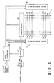
- Fig. 3 is a diagram showing the internal constitutions of The X-row electrode driver 7 and the Y-row electrode driver 8, respectively.
- the X-row electrode driver 7 comprises a power source B1 for generating a direct current voltage V S1 , which constitutes the source of pulse voltage for a driving pulse.
- the positive terminal of power source B1 is connected to row electrode X of PDP 10 via a switching element S3, and the negative terminal thereof is grounded.
- a switching element S4 selectively grounds row electrode X.
- One end of a condenser C1 is grounded, and a first serial circuit comprising a coil L1, a diode D1 and a switching element S1, and a second serial circuit comprising a coil L2, a diode D2 and a switching element S2 are connected in parallel between the other end of condenser C1 and row electrode X.
- the X-row electrode driver 7 is equipped with a resetting pulse generator RX comprising a variable resistor R1, a switching element S5 and a power source B2.
- Power source B2 generates a direct current voltage V r for carrying the pulse voltage of a resetting pulse RP X , which will be described hereinbelow.
- the positive terminal of power source B2 is grounded, and the negative terminal is connected to the switching element S5.
- the switching element S5 applies a negative direct current voltage -V r generated by the negative terminal of power source B2 to row electrode X of PDP 10 via variable resistor R1 only while it is set to the ON state.
- variable resistor R1 is set to a resistance value in accordance with the resetting pulse waveform adjusting signal RW supplied from the above-mentioned drive controller 4.
- the Y-row electrode driver 8 comprises a power source B3 for generating a direct current voltage V S1 , which constitutes the source of pulse voltage for a driving pulse.
- the positive terminal of power source B3 is connected to a connection line 12 to a switching element S15 via a switching element S13, and the negative terminal thereof is grounded.
- Connection line 12 is grounded via the switching element S14.
- One end of a condenser C2 is grounded, and a first serial circuit comprising a coil L3, a diode D3 and a switching element S11, and a second serial circuit comprising a coil L4, a diode D4 and a switching element S12 are connected in parallel between the other end of condenser C2 and connection line 12.
- the switching element S15 makes the connection between connection line 12 and connection line 13 when it is in the ON state, and breaks the connection between these two when it is in the OFF state.
- the positive terminal of a power source B6, which generates a direct current voltage V n , a switching element S21, and the cathode terminal of a diode D5 are connected to this connection line 13.
- a switching element S22 and the anode terminal of diode D6 are connected to the negative terminal of power source B6.
- the cathode terminal of diode D6, the anode terminals of diode D5 and the switching elements S21 and S22 are interconnected, and row electrode Y of PDP 10 is connected to the connection point thereof.
- the Y-row electrode driver 8 is equipped with a resetting pulse generator RY comprising a variable resistor R2, a switching element S16 and a power source B4.
- Power source B4 generates a direct current voltage V r for carrying the pulse voltage of a resetting pulse RP Y , which will be described hereinbelow.
- the negative terminal of power source B4 is grounded, and the positive terminal is connected to the switching element S16.
- the switching element S16 applies direct current voltage V r generated by the positive terminal of power source B4 to the above-mentioned connection line 13 via variable resistor R2 only while it is set to the ON state.
- variable resistor R2 is set to a resistance value in accordance with the resetting pulse waveform adjusting signal RW supplied from the above-mentioned drive controller 4.
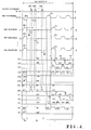
- Fig. 4 is a figure showing the respective switching operations of the above-mentioned switching elements S1 through S5, S11 through S16, S21 and S22 in accordance with the various switching signals supplied from the drive controller 4, the various driving pulses generated in accordance with these switching operations, and the application timing thereof. Furthermore, in Fig. 4, only the operation inside the lead subfield SF1 in the emission driving format shown in Fig. 2 is excerpted and shown.
- the drive controller 4 sets the switching element S5 of The X-row electrode driver 7 and the switching elements S16 and S21 of The Y-row electrode driver 8, respectively, to the ON state, and sets other switching elements to the OFF state.
- the switching element S5 of The X-row electrode driver 7 being set to the ON state, current flows into the path comprising row electrode X, variable resistor R1, the switching element S5 and power source B2.
- the voltage across row electrode X steadily drops at an inclination that accords with a time constant based on the load capacitance C0 between the row electrodes of PDP 10 and the resistance value of variable resistor R1.
- the switching element S16 of The Y-row electrode driver 8 being set to the ON state, current flows into row electrode Y of PDP 10 via power source B4, the switching element S16, variable resistor R2, and the switching element S21.
- the voltage across row electrode Y steadily rises at an inclination that accords with a time constant based on the load capacitance C0 between the row electrodes of PDP 10 and the resistance value of variable resistor R2.
- the drive controller 4 switches the switching element S5 to the OFF state and the switching element S4 to the ON state, respectively, at the timing at which the voltage across row electrode X reaches negative voltage -V r based on direct current voltage V r generated by power source B2.
- a resetting pulse RP X the level change of the leading edge (at rise time) of which reaches negative voltage -V r more slowly than the respective scanning pulse SP and sustaining pulse IP, which will be described hereinbelow, is generated. Then, this resetting pulse RP X is applied simultaneously to each of the row electrodes X 1 through X n .
- the drive controller 4 switches the switching element S16 to the OFF state and the switching elements S14 and S15 to the ON state, respectively, at the timing at which the voltage across row electrode Y reaches direct current voltage V r generated by power source B4.
- a resetting pulse RP y the level change of the leading edge (at rise time) of which reaches positive voltage V r more slowly than the respective scanning pulse SP and sustaining pulse IP, which will be described hereinbelow, is generated. Then, this resetting pulse RP y is applied simultaneously to each of the row electrodes Y 1 through Y n .
- all the discharge cells of PDP 10 are subjected to reset discharging, and following the cessation of this discharging, a wall charge of a predetermined amount is uniformly formed and held inside each discharge cell.
- all discharge cells in PDP 10 are initialized to an emission (sustain discharge)-enabled state (hereinafter referred to as an light-emitting cell state) in an emission sustaining step Ic, which will be explained hereinbelow.
- the address driver 6 generates a pixel data pulse having a pulse voltage that accords with the pixel driving data bit DB1 supplied from the above-mentioned memory 3. For example, when the logic level of a pixel driving data bit DB is "1", the address driver 6 generates a high voltage, and when the logic level is "0", it generates a low voltage (0 volts). Then, the address driver 6 sequentially applies a pixel data pulse group DP 1 , DP 2 , ..., DP n , which groups the above-mentioned pixel data pulses by individual display line (m lines), to column electrodes D 1 through D m .
- the Y-row electrode driver 8 generates a negative scanning pulse SP at the same timing as the application timing of each of the above-mentioned pixel data pulse groups DP 1 through DP n , and sequentially applies this to row electrodes Y 1 through Y n . Furthermore, this scanning pulse SP, as shown in Fig. 4, is generated by setting the above-mentioned the switching element S21 to the OFF state, and the switching element S22 to the ON state. In this process, a discharge (selective erase discharge) takes place only in the discharge cell at the intersecting portion of the display line to which the above-mentioned scanning pulse was applied, and the "column" to which a high voltage pixel data pulse was applied.
- the wall charge being held inside the discharge cell is erased by this selective erase discharge, and this discharge cell is set to a state, wherein an emission (sustain discharge) cannot be performed in an emission sustaining step Ic, which will be explained hereinbelow (hereinafter referred to as a non-light-emitting cell state).
- an emission sustain discharge
- Ic emission sustaining step
- the above-mentioned selective erase discharge does not occur in a discharge cell to which a low-voltage pixel data pulse is applied while a scanning pulse SP is being applied, and this discharge cell is maintained in the state to which it was initialized in the above-mentioned simultaneous resetting step Rc, that is, an light-emitting cell state.
- each discharge cell of PDP 10 is set to either one of an light-emitting cell state or a non-light-emitting cell state in accordance with input picture signal-based pixel data.
- positive sustaining pulses IP X and IP Y are generated by operating the switching elements S1 through S4 and S11 through S14 inside the X-row electrode driver 7 and the Y-row electrode driver 8, respectively, in an ON-OFF sequence like that shown in the figure.
- the respective The X-row electrode driver 7 and the Y-row electrode driver 8 alternately apply these positive sustaining pulses IP X and IP Y repeatedly to row electrodes X and Y.
- the number (or period) of sustaining pulses to be applied in each emission sustaining step Ic is set in accordance with the weighting of each subfield.
- the emission always occurs in an emission sustaining step IC of subfield SF1, except when representing brightness level 0, and thereafter, continuous emission occurs in the emission sustaining steps Ic of each subfield SF in proportion to a number that accords with the brightness level to be represented. That is, the brightness of the grayscale levels can be represented at the (N + 1) stage according to N subfields SF1 through SF(N), including cases when brightness level 0 is represented by sustaining all subfields in a lights-out state.
- the reset discharge which occurs for all discharge cells in the above-mentioned simultaneous resetting step Rc, is a relatively strong discharge, and is accompanied by an emission having a high brightness level. Since this reset discharge occurs simultaneously for all discharge cells irrespective of pixel data, it is the cause of a reduction in dark contrast.
- the constitution is such that the intensity of a reset discharge is appropriately adjusted in accordance with the ambient lightness of PDP 10.
- the external light sensor 5 supplies an illuminance signal LL having a signal level that accords with the lightness of this room to the drive controller 4.
- the drive controller 4 supplies a resetting pulse waveform adjusting signal RW to the X-row electrode driver 7 and the Y-row electrode driver 8 for setting the level change of the leading edge of each of the resetting pulses RP X and RP Y to an inclination corresponding to the above-mentioned illuminance signal LL.
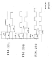
- variable resistors R1 and R2 respectively disposed in the resetting circuits RX and RY of the X-row electrode driver 7 and the Y-row electrode driver 8, respectively, are set to resistance values corresponding to this resetting pulse waveform adjusting signal RW. Accordingly, in this process, resetting circuits RX and RY generate the resetting pulses RP X and RP Y like those shown in Fig. 5B, in which the level change rate at the leading edge constitutes a waveform corresponding to the resetting pulse waveform adjusting signal RW.
- the external light sensor 5 supplies to the drive controller 4 a high-level illuminance signal LL corresponding to the lightness of this room.
- the drive controller 4 supplies a resetting pulse waveform adjusting signal RW to the X-row electrode driver 7 and the Y-row electrode driver 8 for setting the level change at the leading edge of each of the resetting pulses RP X and RP Y to make them slope steeply in proportion to an extent corresponding to the above-mentioned illuminance signal LL.
- variable resistors R1 and R2 inside the resetting circuits RX and RY become small in accordance with this resetting pulse waveform adjusting signal RW, and the time constant becomes small. Accordingly, in this process, the resetting circuit RX (or RY) generates the resetting pulses RP X and RP Y of waveforms such as those shown in Fig. 5A, in which the level change rate at the leading edge is great compared to the waveform shown in Fig. 5B, that is, the time period until the waveform reaches voltage -V r (or V r ) is short. By simultaneously applying these resetting pulses RP X and RP Y , a relatively strong reset discharge occurs in all the discharge cells.
- the external light sensor 5 supplies to the drive controller 4 a low-level illuminance signal LL corresponding to the lightness of this room.
- the drive controller 4 supplies a the resetting pulse waveform adjusting signal RW to the X-row electrode driver 7 and the Y-row electrode driver 8 for setting the level change at the leading edge of each of the resetting pulses RP X and RP Y to make them slope gently in proportion to an extent corresponding to the above-mentioned illuminance signal LL.
- variable resistors R1 and R2 inside the resetting circuits RX and RY become large in accordance with this resetting pulse waveform adjusting signal RW, and the time constant becomes large. Accordingly, at this time, the resetting circuit RX (or RY) generates the resetting pulses RP X and RP Y of waveforms such as those shown in Fig. 5C, in which the level change rate at the leading edge is small compared to the waveform shown in Fig. 5B, that is, the time period until the waveform reaches voltage -V r (or V r ) is long.
- the present invention enhances the dark contrast, which makes this image stand out.
- the pulse width of the resetting pulses RP X and RP Y changes as shown in Fig. 5A through Fig. 5C. Accordingly, the drive controller 4 changes the number of sustaining pulses IP X and IP Y to be applied in the emission sustaining step Ic of each subfield in proportion to the extent of change of the pulse widths of the resetting pulses RP X and RP Y . For example, as shown in Fig.
- the drive controller 4 controls The X-row electrode driver 7 and the Y-row electrode driver 8 so as to increase the number of sustaining pulses to be applied inside each subfield when the area around a plasma display panel is relatively light, and to decrease this number of sustaining pulses when this area is dark.
- the present invention can also similarly be applied to a case in which a so-called selective write addressing method, i.e. a method in which wall charges are selectively formed in accordance with pixel data, is employed as the pixel data writing method.
- a so-called selective write addressing method i.e. a method in which wall charges are selectively formed in accordance with pixel data
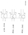
- a negative erasing pulse EP is simultaneously applied to each of row electrodes Y 1 through Y n as shown in Fig. 6A through Fig. 6C.
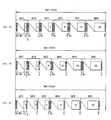
- Fig. 6A through Fig. 6C are diagrams showing the resetting pulses RP X and RP Y to be applied, the waveforms of each erasing pulse EP, and the application timing thereof when the area around PDP 10 is relatively light (Fig. 6A), when this area is within the normal illuminance range (Fig. 6B), and when this area is relatively dark (Fig. 6C), respectively.
- a simultaneous resetting step RC when using the selective write addressing method, the wall charges formed inside all the discharge cells by simultaneously applying the resetting pulses RP Y and RP X are all erased by applying the erasing pulse EP shown in Fig. 6. That is, all of the discharge cells are initialized to a non-emission state in accordance with applying this erasing pulse EP.
- a pixel data writing step Wc when using the selective write addressing method, discharging (a selective write discharge) only takes place in a discharge cell to which a scanning pulse SP and high-voltage pixel data pulse are simultaneously applied as described hereinabove.
- the level change in the leading edge portions of the resetting pulses RP Y and RP X is a curved shape, but as in Fig. 7A through Fig. 7C, this level change can also be linear. In other words, when the area around PDP 10 is relatively bright, the level change at the leading edge portions of the resetting pulses RP Y and RP X is made steep as shown in Fig. 7A, but when this area is dark, this level change is made gentle as shown in Fig. 7C.
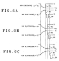
- one reset discharge should be generated within a one field display period, but the number of executions thereof can be changed in accordance with the ambient lightness of the PDP.
- the number of the resetting pulses (RP X1 , RP Y1 , RP Y2 , RP X3 , RP Y4 ) applied in a simultaneous resetting step Rc is set to four as shown in Fig. 8A.
- the number of the resetting pulses (RP X1 , RP Y1 , RP Y2 ) applied in a simultaneous resetting step Rc is set to two as shown in Fig. 8B.
- the emission driving format shown in Fig. 8A through Fig. 8C presents one example of a case in which the selective write addressing method as described hereinabove is used as the pixel data writing method.
- the number of simultaneous resetting steps Rc to be executed within a one field display period can be changed in accordance with the lightness around PDP 10, for example, as shown in Fig. 9A through Fig. 9C.
- a one field display period is divided into six subfields comprising subfields SF1 through SF6, and the driving of the PDP 10 to display images with grayscale levels is implemented using the selective write addressing method.
- a simultaneous resetting step Rc is executed in the respective front positions of all the subfields SF1 through SF6.
- the simultaneous resetting steps Rc are executed in the respective front positions of SF1, SF3 and SF5 of subfields SF1 through SF6, respectively.
- the simultaneous resetting steps Rc are executed in the respective front positions of SF1 and SF4 of subfields SF1 through SF6, respectively.
- the waveforms of the resetting pulses RP X and RP Y generated within all the simultaneous resetting steps Rc shown in Fig. 9A through Fig. 9C, for example, are shown in Fig. 6B.
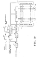
- Fig. 10 is a diagram showing the simplified constitution of a plasma display apparatus equipped with a plasma display panel (hereinafter referred to as PDP).
- this plasma display apparatus is constituted by the PDP 10 as a plasma display panel, and a driving portion comprising various functional modules.
- the PDP 10 comprises m column electrodes D 1 through D m as address electrodes, and n row electrodes X 1 through X n and row electrodes Y 1 through Y n , respectively, which are arranged so as to intersect with these respective column electrodes.
- These row electrodes X 1 through X n and row electrodes Y 1 through Y n support a first display line through an nth display line in PDP 10 for each pair of row electrodes X 1 (1 ⁇ i ⁇ n) and Y 1 (1 ⁇ i ⁇ n).
- a discharge space into which is filled a discharge gas, is formed between a column electrode D and row electrodes X and Y.
- the constitution is such that a discharge cell corresponding to a pixel is formed at each intersecting portion of each row electrode pair and column electrode comprising this discharge space.
- m discharge cells that is, a number equivalent to the number of column electrodes D, exist on a single display line.
- the driving portion is constituted by a synchronism detecting circuit 21, a drive controller 22, an A/D converter 23, memory 24, an address driver 26, a first sustaining driver 27, a second sustaining driver 28, a data converter 30, an external light sensor 51, and a brightness mode setting circuit 52.
- Synchronism detecting circuit 21 generates a vertical synchronism detection signal V when a vertical synchronization signal is detected in an input picture signal, and generates a horizontal synchronism detection signal H when a horizontal synchronization signal is detected in an input picture signal, and supplies the same to the drive controller 22.
- the A/D converter 23 samples an input picture signal, converts this, for example, to 8-bit pixel data PD corresponding to each pixel, and supplies this to data converter 30.
- Data converter 30 performs processing for increasing shades of gradation on the pixel data, and thereafter converts this processed pixel data to 8-bit pixel driving data GD for setting each discharge cell of PDP 10 to either the light-emitting cell state or the non-light-emitting cell state, and supplies this to memory 24.
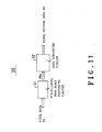
- Fig. 11 is a diagram showing an example of the internal constitution of this data converter 30.
- a multi-level gray scale processing circuit 31 performs error diffusion processing and dithering on 8-bit pixel data. For example, in the above-mentioned error diffusion processing, first, the upper six bits of pixel data are captured as display data, and the remaining lower two bits are captured as error data. Then, the weighting of each error data of the above-mentioned pixel data PD corresponding to the respective neighboring pixels is added, and this is reflected in the above-mentioned display data.
- the brightness of the lower two bits in the original pixel is falsely represented by the above-mentioned neighboring pixels, making it possible to represent the same brightness gradation as the above-mentioned 8-bit pixel data in the 6-bit display data, which is less than eight bits.
- dithering is performed for the 6-bit error diffusion processed pixel data achieved via this error diffusion processing.
- a plurality of pixels located adjacent to one another are treated as a single pixel unit, and dithering coefficients comprising mutually different coefficients are respectively allocated and added to the above-mentioned error diffusion processed pixel data corresponding to each pixel inside this single pixel unit, respectively, to achieve dithered pixel data.
- multi-level gray scale processing circuit 31 supplies the upper four bits of the above-mentioned dithered pixel data to data converting circuit 32 as pixel data with increased shades PD S .
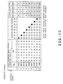
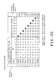
- Data converting circuit 32 converts the above-mentioned four bits of pixel data with increased shades PD S to 8-bit pixel driving data GD in accordance with a data conversion table as shown in Fig. 12, and supplies this to memory 24. Furthermore, the first through the eighth bits of pixel driving data GD, respectively, correspond to the respective subfields SF1 through SF8, which will be explained hereinbelow.
- Memory 24 sequentially writes in the above-mentioned pixel driving data GD in accordance with write signals supplied from the drive controller 22. Then, when a write of one screen's worth of pixel driving data, that is, (n x m) worth of pixel driving data from pixel driving data GD 11 corresponding to pixels of the first line and first column to pixel driving data GD nm corresponding to pixels of the nth line and mth column, is complete, memory 24 performs a read-out operation as follows.
- memory 3 captures the first screen's worth of written pixel driving data GD 11 through GD nm , respectively, as pixel driving data bits DB1 through DB8, which are divided into respective bit digits (first bit through eighth bit).
- memory 24 reads out the above-mentioned pixel driving data bits DB1 11 through DB1 nm one display line at a time, and supplies them to the address driver 26.
- memory 24 reads out the above-mentioned pixel driving data bits DB2 11 through DB2 nm one display line at a time, and supplies them to the address driver 26.
- memory 24 reads out pixel driving data bits DB3 through DB8 one display line at a time at the timing of the respective pixel data writing steps Wc of subfields SF3 through SF8, which will be explained hereinbelow, and supplies them to the address driver 26.
- the external light sensor 51 is a sensor disposed in the area around the above-mentioned PDP 10, and detects the ambient lightness of PDP 10, and supplies an illuminance signal LL having a signal level corresponding to this lightness to the brightness mode setting circuit 52.
- the brightness mode setting circuit 52 supplies to the drive controller 22 a brightness mode signal LC indicating brightness mode 1 when the lightness around PDP 10 represented by the above-mentioned illuminance signal LL is darker than a prescribed illuminance L1. Furthermore, brightness mode setting circuit 52 supplies to the drive controller 22 a brightness mode signal LC indicating brightness mode 2 when the lightness around PDP 10 represented by this illuminance signal LL is lighter than prescribed illuminance L1 but darker than prescribed illuminance L2. Furthermore, brightness mode setting circuit 52 supplies to the drive controller 22 a brightness mode signal LC indicating brightness mode 3 when the lightness around PDP 10 represented by this illuminance signal LL is lighter than prescribed illuminance L2 but darker than prescribed illuminance L3.
- brightness mode setting circuit 52 sets four stages of brightness modes corresponding to the illuminance around PDP 10, that is, the lightness of the place in which PDP 10 is installed, in the drive controller 22.
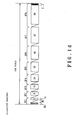
- the drive controller 22 supplies various timing signals t the address driver 26, the first sustaining driver 27 and the second sustaining driver 28 respectively, for controlling the driving of PDP 10 in accordance with the emission driving format shown in Fig. 14 and the above-mentioned brightness mode signals LC.
- the display period of each field (hereinafter a representation comprising a single frame as well) is divided into eight subfields SF1 through SF8. Then a pixel data writing step Wc for setting each discharge cell of PDP 10 to at the least one of either an light-emitting cell state or a non-light-emitting cell state, and an emission sustaining step Ic for causing only discharge cells, which are in the above-mentioned light-emitting cell state, to repeatedly emit light only the number of times indicated by the frequency ratio described inside Fig. 14, are implemented inside each subfield.
- a simultaneous resetting step Rc for initializing the wall charge quantity inside all the discharge cells of PDP 10 is executed only in the front of lead subfield SF1, and erasing step E for simultaneously erasing the wall charges inside all the discharge cells is executed at the very end of final subfield SF8.
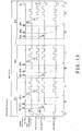
- Fig. 15 is a diagram showing the various drive pulses, which the above-mentioned address driver 26, first sustaining driver 27 and second sustaining driver 28 apply to PDP 10, and the application timing thereof in the above-mentioned simultaneous resetting step Rc, pixel data writing step Wc, emission sustaining step Ic and erasing step E.
- resetting pulses RP X and RP Y all the discharge cells inside PDP 10 are subjected to reset discharging, and immediately after this reset discharging, a wall charge of a predetermined quantity is uniformly formed inside each discharge cell. This reset discharging initializes all the discharge cells to the light-emitting cell state.
- the address driver 26 generates a pixel data pulse having a voltage corresponding to the logic level of the pixel driving data bit DB supplied from the above-mentioned memory 24. For example, when the logic level of a pixel driving data bit DB is "1", the address driver 26 generates a high voltage pixel data pulse, and when the logic level is "0", it generates a low voltage (0 volts) pixel data pulse. At this time, the address driver 26 applies pixel data pulses generated as described hereinabove to column electrodes D 1 through D m one line (m electrodes) at a time.
- the address driver 26 first extracts an amount corresponding to the first line, that is DB1 11 through DB1 1m , from thereamong. Then, the address driver 26 converts each of these m bits of DB1 11 through DB1 1m to m pixel data pulses DB1 11 through DB1 1m corresponding to the logic level thereof, and simultaneously applies these pulses to column electrodes D 1 through D m as shown in Fig. 15.
- the address driver 26 extracts pixel driving data bits DB1 21 through DB1 2m corresponding to the second line from among pixel driving data bit group DB1 11 through DB1 nn . Then, the address driver 26 converts each of these m bits of DB1 21 through DB1 2m to m pixel data pulses DB1 21 through DB1 2m corresponding to the logic level thereof, and simultaneously applies these pulses to column electrodes D 1 through D m as shown in Fig. 15. Thereafter, in the pixel data writing step Wc of subfield SF1, the address driver 26 similarly applies pixel data pulse DP1 corresponding to pixel driving data bit DB1 supplied from memory 24 to column electrodes D 1 through D m one line at a time.
- second sustaining driver 28 generates a negative scanning pulse SP as shown in Fig. 15 at the same timing as the application timing of the one-line-at-a-time pixel data pulse DP as described hereinabove, and sequentially applies this to row electrodes Y 1 through Y n .
- a discharge selective erase discharge
- discharge cells which were initialized to the light-emitting cell state in the above-mentioned simultaneous resetting step Rc, are set to the non-light-emitting cell state.
- discharge cells in which the above-mentioned selective erase discharge did not take place retain the state of immediately prior thereto. That is, discharge cells, which were in the light-emitting cell state, are set to the light-emitting cell state as-is, and discharge cells, which were in the non-light-emitting cell state, are set to the non-light-emitting cell state as-is.
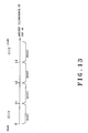
- the address driver 26 and second sustaining driver 28 when the above-mentioned brightness mode signal LC indicates brightness mode 1, the address driver 26 and second sustaining driver 28 generate a pixel data pulse and a scanning pulse SP of pulse width T1 as shown in Fig. 16A. Furthermore, when the above-mentioned brightness mode signal LC indicates brightness mode 2, the address driver 26 and second sustaining driver 28 generate a pixel data pulse and a scanning pulse SP of pulse width T2, which is narrower than the above-mentioned pulse width T1, as shown in Fig. 16B.
- the address driver 26 and second sustaining driver 28 when the above-mentioned brightness mode signal LC indicates brightness mode 3, the address driver 26 and second sustaining driver 28 generate a pixel data pulse and a scanning pulse SP of pulse width T3, which is narrower than the above-mentioned pulse width T2, as shown in Fig. 16C. Furthermore, when the above-mentioned brightness mode signal LC indicates brightness mode 4, the address driver 26 and second sustaining driver 28 generate a pixel data pulse and a scanning pulse SP of pulse width T4, which is narrower than the above-mentioned pulse width T3, as shown in Fig. 16D.
- the address driver 26 and second sustaining driver 28 generate pixel data pulses and scanning pulses SP with wider pulse widths the darker the area around PDP 10 is.
- the wider the pulse width of the pixel data pulses and scanning pulses SP the higher the discharge margin for the above-mentioned selective erase discharge.
- the discharge margin becomes high, it becomes possible to reliably cause a selective erase discharge to occur, even, for example, when the priming particle weight that exists inside a discharge cell is low.
- first sustaining driver 27 and second sustaining driver 28 alternately apply positive sustaining pulses IP X and IP Y to row electrodes X 1 through X n and Y 1 through Y n as shown in Fig. 15.
- the number of the above-mentioned sustaining pulses IP repeatedly applied in the emission sustaining step Ic of each of subfields SF1 through SF8 is based on the brightness mode indicated by the above-mentioned brightness mode signal LC.
- a brightness mode signal LC indicates brightness mode 1
- the number of the above-mentioned sustaining pulses IP repeatedly applied in the emission sustaining step Ic of each of subfields SF1 through SF8 is as shown in Fig. 18, which is
- a brightness mode signal LC indicates brightness mode 2
- the number of the above-mentioned sustaining pulses IP repeatedly applied in the emission sustaining step Ic of each of subfields SF1 through SF8 is as shown in Fig. 18, which is
- a brightness mode signal LC indicates brightness mode 3
- the number of the above-mentioned sustaining pulses IP repeatedly applied in the emission sustaining step Ic of each of subfields SF1 through SF8 is as shown in Fig. 18, which is
- a brightness mode signal LC indicates brightness mode 4
- the number of the above-mentioned sustaining pulses IP repeatedly applied in the emission sustaining step Ic of each of subfields SF1 through SF8 is as shown in Fig. 18, which is
- first sustaining driver 27 and second sustaining driver 28 when the above-mentioned brightness mode signal LC indicates brightness mode 1, first sustaining driver 27 and second sustaining driver 28 generate sustaining pulses IP X and IP Y of pulse width P1 as shown in Fig. 17A. Furthermore, when brightness mode signal LC indicates brightness mode 2, first sustaining driver 27 and second sustaining driver 28 generate sustaining pulses IP X and IP Y of pulse width P2, which, as shown in Fig. 17B, is narrower than the above-mentioned pulse width P1. Furthermore, when brightness mode signal LC indicates brightness mode 3, first sustaining driver 27 and second sustaining driver 28 generate sustaining pulses IP X and IP Y of pulse width P3, which, as shown in Fig.
- first sustaining driver 27 and second sustaining driver 28 generate sustaining pulses IP X and IP Y of pulse width P4, which, as shown in Fig. 17D, is narrower than the above-mentioned pulse width P3.
- first sustaining driver 27 and second sustaining driver 28 generate sustaining pulses IP X and IP Y , the pulse widths of which are wider the darker the area around PDP 10 is.
- the wider the pulse width of sustaining pulses IP X and IP Y the higher the discharge margin is when the above-mentioned sustain discharge occurs.
- this discharge margin is high, it becomes possible to reliably cause a sustain discharge to occur, even, for example, when the priming particle weight that exists inside a discharge cell is low.
- discharge cells in which the wall charge remains as-is that is, discharge cells that were set to the light-emitting cell state in the above-mentioned pixel data writing step Wc, are subjected to a sustain discharge each time the above-mentioned sustaining pulses IP X and IP Y are applied, and the emission cell state accompanying this sustain discharge is maintained only for the number of discharges allocated for each subfield.
- whether or not each discharge cell is set to the light-emitting cell state is determined by pixel driving data GD.
- the patterns capable of being adopted as the pixel driving data GD are the nine patterns shown in Fig. 12.
- the only step that is capable of forming a wall charge inside a discharge cell, and switching this discharge cell from the non-light-emitting cell state to the light-emitting cell state is the simultaneous resetting step Rc in the lead subfield SF1. Consequently, according to driving that makes use of the pixel driving data GD of Fig. 12, a discharge cell is held in the light-emitting cell state for the period from the head of each field until a selective erase discharge occurs in the pixel data writing step Wc of the subfields marked with a black circle in Fig. 15. Then, when a selective erase discharge occurs one time, thereafter, the discharge cell is held in a non-light-emitting cell state until the very end of one field. Accordingly, each discharge cell is held in the light-emitting cell state until the first selective erase discharge takes place inside each field, and consecutive sustain discharges occur in the emission sustaining steps Ic of each subfield (indicated by white circles) that exists therebetween.
- a brightness mode signal LC indicates brightness mode 1
- a nine-gray-level intermediate brightness display having visible brightness comprising ⁇ 0, 1, 7, 23, 47, 82, 128, 185, 255 ⁇ is achieved.
- a brightness mode signal LC indicates brightness mode 2
- a nine-gray-level intermediate brightness display having visible brightness comprising ⁇ 0, 2, 14, 46, 94, 164, 256, 370, 510 ⁇ is achieved.
- a brightness mode signal LC indicates brightness mode 3
- a nine-gray-level intermediate brightness display having visible brightness comprising ⁇ 0, 3, 21, 69, 141, 246, 384, 555, 765 ⁇ is achieved.
- a brightness mode signal LC indicates brightness mode 4
- a nine-gray-level intermediate brightness display having visible brightness comprising ⁇ 0, 4, 28, 92, 188, 328, 512, 740, 1020 ⁇ is achieved.
- the present invention is constituted such that various discharges are made to occur reliably by reducing the number of sustain discharges that take place in the emission sustaining step of each subfield when the area around PDP 10 is dark as compared to when it is light, and, in addition, widening the respective pulse widths of scanning pulses, pixel data pulses and sustaining pulse to that extent.
- the respective pulse widths of scanning pulses, pixel data pulses and sustaining pulses are changed in accordance with the illuminance of the area surrounding PDP 10.
- the constitution is such that the number of sustaining pulses per unit time repeatedly applied to cause the respective discharge cells to emit light is changed, and, in addition, the pulse width of at the least one of either the scanning pulse or the sustaining pulse is adjusted in accordance with the luminous intensity around the plasma display panel. Consequently, when the area around the plasma display panel is dark, if the number of sustaining pulses per unit time is reduced, and, in addition, the pulse width of at the least one of either the scanning pulse or the sustaining pulse is widened, power consumption can be reduced while also assuring reliable discharge operations.
- Fig. 1 is a diagram showing the simplified constitution of a plasma display apparatus equipped with a plasma display panel (hereinafter referred to as PDP).
- PDP plasma display panel
- this plasma display apparatus is constituted from PDP 10 as a plasma display panel, and a driving portion comprising various functional modules.
- the driving portion is constituted from an A/D converter 23, a drive controller 22, a memory 24, an address driver 26, a first sustaining driver 27, a second sustaining driver 28, a data converter 30, an average brightness computing circuit 50, an external light sensor 51, and a memory for ABL characteristics 53.
- the A/D converter 23 samples an input picture signal, converts this, for example, to 8-bit pixel data PD corresponding to each pixel, and supplies this to the data converter 30 and average brightness computing circuit 50, respectively.
- the data converter 30 performs the multi-level gray scale processing on pixel data PD, after which, it converts this pixel data PD to 8-bit pixel driving data GD for setting each discharge cell on the PDP 10 to either the light-emitting cell state or the non-light-emitting cell state in each subfield, and supplies this data to the memory 24.
- the Data converter 30 is the same as that shown in Fig. 11, and an explanation thereof will not be reiterated.
- the data converter 30 converts the above-mentioned multi-grayscale pixel data PD S of four bits to pixel driving data GD of eight bits in accordance with a data conversion table as shown in Fig. 20, and supplies this to memory 24.
- Average brightness computing circuit 50 computes the average brightness level of an image according to an input picture signal based on one field's worth of the above-mentioned pixel data PD for each field (each frame), and supplies an average brightness signal APL indicating this computed average brightness level to the drive controller 22.
- the external light sensor 51 is a sensor disposed in the area around the above-mentioned PDP 10, and detects the ambient lightness around PDP 10, and supplies an illuminance signal LL having a signal level corresponding to this lightness to the drive controller 22.
- the ABL (Automatic Brightness Limiting) characteristics memory 53 there is stored a data conversion table corresponding to three ABL characteristics A through C, respectively, as shown in Fig. 21, for converting the above-mentioned average brightness signal APL to a number of sustaining pulses to be applied to discharge cells inside each field, that is, an application frequency.
- a data conversion table based on ABL characteristic A when an average brightness signal APL is smaller than a first lower limit V1, a sustaining pulse application number of, for example, "1530" is obtained, and conversely, when an average brightness signal APL is larger than the above-mentioned first lower limit V1, an number of applications that is as small as the average brightness signal APL is large is obtained.
- the power consumed pursuant to a sustain discharge is held within a predetermined first power consumption regardless of the average brightness of an input picture.
- a sustaining pulse application number of, for example, "1530" is obtained, and conversely, when an average brightness signal APL is larger than the above-mentioned second lower limit V2, an number of applications that is as small as the average brightness signal APL is large is obtained.
- consumed power which is consumed pursuant to a sustain discharge, is held within a predetermined second power consumption regardless of the average brightness of an input picture.
- a sustaining pulse application number of "1530" is obtained, and conversely, when an average brightness signal APL is larger than the above-mentioned third lower limit V3, an number of applications that is as small as the average brightness signal APL is large is obtained.
- consumed power which is consumed pursuant to a sustain discharge, is held within a predetermined third power consumption regardless of the average brightness of an input picture.
- the ABL characteristics A through C changes the number of applications of sustaining pulses to be applied to discharge cells inside each field, that is, the application frequency, to a number that is as small as the average brightness of an input picture is high, to limit the respective power consumed pursuant to a sustain discharge to within a separately set predetermined power consumption.
- the above-mentioned first lower limit Vlin The ABL characteristic A is the highest, followed by the second lower limit V2 in The ABL characteristic B, and the third lower limit V3 in The ABL characteristic C. Therefore, the above-mentioned second power consumption according to the above-mentioned ABL characteristic B is smaller than the above-mentioned first power consumption according to the above-mentioned ABL characteristic A, and the above-mentioned third power consumption according to the above-mentioned ABL characteristic C is smaller than the above-mentioned second power consumption.
- the ABL characteristics memory 53 selectively reads out, from among The ABL characteristics A through C, a data conversion table of The ABL characteristics indicated by an ABL characteristic read-out signal supplied from the drive controller 22, and supplies this to the drive controller 22.
- the drive controller 22 supplies various timing signals for driving and controlling PDP 10 in accordance with the emission driving format shown in Fig. 14, to the address driver 26, first sustaining driver 27 and second sustaining driver 28, respectively.
- the first sustaining driver 27 and second sustaining driver 28 alternately apply positive sustaining pulses IP X and IP Y to row electrodes X 1 through X n and Y 1 through Y n as shown in Fig. 15.
- the number of times that the above-mentioned sustaining pulses IP is repeatedly applied in the emission sustaining step Ic of each of subfields SF1 through SF8 is based on the above-mentioned average brightness signal APL, illuminance signal LL and data conversion tables read out from The ABL characteristics memory 53.
- the drive controller 22 supplies an ABL characteristic read-out signal for reading out a data conversion table corresponding to the ABL characteristic C to the ABL characteristic memory 53.
- the ABL characteristic memory 53 supplies a data conversion table corresponding to the ABL characteristic C as shown in Fig. 21 to the drive controller 22.
- the drive controller 22 determines the number of applications of sustaining pulses corresponding to average brightness signal APL based on the above-mentioned data conversion table corresponding to the ABL characteristic C.
- the drive controller 22 allocates the number of applications of sustaining pulses to be applied within this one field display period to the emission sustaining step Ic of each subfield as a frequency ratio as shown in Fig. 14, and supplies the timing signal for these sustaining pulses to the first sustaining driver 27 and the second sustaining driver 28, respectively.
- the average brightness signal APL for example, is "40" as shown in Fig. 21
- "510" will be obtained as the total number of sustaining pulses to be applied inside a one field display period. Consequently, when this pulse number for sustaining pulses of "510" is allocated to the emission sustaining step Ic of the respective subfields SF1 through SF8 as a frequency ratio as shown in Fig. 14, as shown in Fig. 23, this frequency ratio becomes:
- the drive controller 22 supplies to the ABL characteristic memory 53 an ABL characteristic read-out signal for reading out a data conversion table corresponding to the ABL characteristic B.
- the ABL characteristic memory 53 supplies a data conversion table corresponding to the ABL characteristic B as shown in Fig. 21 to the drive controller 22.
- the drive controller 22 determines the number of applications of sustaining pulses corresponding to average brightness signal APL (to be applied within display period of one field) based on the above-mentioned data conversion table corresponding to the ABL characteristic B.
- the drive controller 22 allocates the number of applications of sustaining pulses to be applied within this one field display period to the emission sustaining step Ic of each subfield as a frequency ratio as shown in Fig. 14, and supplies the timing signal for each sustaining pulse to the first sustaining driver 27 and second sustaining driver 28, respectively.
- the average brightness signal APL for example, is "40" as shown in Fig. 21
- the ABL characteristic B "765" will be obtained as the total number of sustaining pulses to be applied inside a one field display period. Consequently, when this pulse number for sustaining pulses of "765" is allocated to the emission sustaining step Ic of the respective subfields SF1 through SF8 as a frequency ratio as shown in Fig. 14, as shown in Fig. 23, this frequency ratio becomes:
- the drive controller 22 supplies an ABL characteristic read-out signal to the ABL characteristic memory 53 for reading out a data conversion table corresponding to the ABL characteristic A.
- the ABL characteristic memory 53 supplies the drive controller 22 with a data conversion table corresponding to the ABL characteristic A as shown in Fig. 21.
- the drive controller 22 determines the number of applications of sustaining pulses corresponding to average brightness signal APL (to be applied within display period of one field) based on the above-mentioned data conversion table corresponding to the ABL characteristic A.
- the drive controller 22 allocates the number of applications of sustaining pulses to be applied within this one field display period to the emission sustaining step Ic of each subfield as a frequency ratio as shown in Fig. 14, and supplies the timing signal for each sustaining pulse to the first sustaining driver 27 and the second sustaining driver 28, respectively.
- the average brightness signal APL for example, is "40" as shown in Fig. 21
- the ABL characteristic A "1020" will be obtained as the total number of sustaining pulses to be applied inside a one field display period. Consequently, when this pulse number for sustaining pulses of "1020" is allocated to the emission sustaining step Ic of the respective subfields SF1 through SF8 as a frequency ratio as shown in Fig. 14, as shown in Fig. 23, this frequency ratio becomes:
- the first sustaining driver 27 and second sustaining driver 28 respectively, repeatedly apply sustaining pulses IP X and IP Y to each discharge cell only the number of times described hereinabove.
- discharge cells in which the wall charge remains unchanged that is, discharge cells that were set to the light-emitting cell state in the above-mentioned pixel data writing step Wc, are subjected to a sustain discharge each time the above-mentioned sustaining pulses IP X and IP Y are applied, and the emission cell state accompanying this sustain discharge is maintained only for the number of discharges allocated for each subfield.
- whether or not each discharge cell is set to the light-emitting cell state is determined by pixel driving data GD.
- the patterns capable of being adopted as the pixel driving data GD are the nine patterns shown in Fig. 20.
- the only step that is capable of forming a wall charge inside a discharge cell, and switching this discharge cell from the non-light-emitting cell state to the light-emitting cell state is the simultaneous resetting step Rc in the lead subfield SF1. Consequently, according to driving that makes use of the pixel driving data GD of Fig. 20, a discharge cell is held in the light-emitting cell state for the period from the head of each field until a selective erase discharge occurs in the pixel data writing step Wc of the subfields marked with a black circle in Fig. 20.
- each discharge cell is held in the light-emitting cell state until the first selective erase discharge takes place inside each field, and consecutive sustain discharges occur in the emission sustaining step Ic of each subfield (indicated by white circles) that exists therebetween.
- an number of applications of sustaining pulses to be applied to each discharge cell within a one field display period is determined based on The ABL characteristic A shown in Fig. 21. Accordingly, when the average brightness level of an input picture as shown in Fig. 21 is "40" for example, the number of applications of sustaining pulses to be applied to each discharge cell inside a one field display period constitutes "1020". Therefore, the brightness levels of the intermediate brightness of the respective nine grayscale levels achieved by emission driving patterns like the nine shown in Fig. 20 become: ⁇ 0, 4, 28, 92, 188, 328, 512, 740, 1020 ⁇
- the illuminance around PDP 10 is relatively high the same as described hereinabove, and the average brightness level of an input picture as shown in Fig. 21 is "50", the number of applications of sustaining pulses to be applied to each discharge cell inside a one field display period constitutes "765". Therefore, the brightness levels of the intermediate brightness of the respective nine grayscale levels achieved by emission driving patterns like the nine shown in Fig. 20 become: ⁇ 0, 3, 21, 69, 141, 246, 384, 555, 765 ⁇
- the number of applications of sustaining pulses applied to each discharge cell inside a one field display period decreases to the extent that the average brightness level of an input picture increases.
- the power limiting operation of the invention works so as to keep this consumed power within the above-mentioned first power consumption.
- an number of applications of sustaining pulses to be applied to each discharge cell within a one field display period is determined based on The ABL characteristic C shown in Fig. 21. Accordingly, for example, when the average brightness level of an input picture as shown in Fig. 21 is "40", the number of applications of sustaining pulses to be applied to each discharge cell inside a one field display period constitutes "510". Therefore, the brightness levels of the intermediate brightness of the respective nine grayscale levels achieved by emission driving patterns like the nine shown in Fig. 20 become: ⁇ 0, 2, 14, 46, 94, 164, 256, 370, 510 ⁇
- the present invention is constituted such that an appropriate screen brightness, which corresponds to the lightness of a place in which the plasma display apparatus is installed, is provided.
- the present invention is constituted such that this consumed power is kept within the above-mentioned third power consumption.
- the third power consumption according to this ABL characteristic C is smaller than the first power consumption according to the ABL characteristic A, which is utilized when the illuminance around PDP 10 is high. Therefore, when the illuminance around PDP 10 is low, the power consumed thereby is lower than when this illuminance is high.
- the ABL characteristics A through C can be adopted as one conversion function for determining the number of applications, that is, the application frequency of sustaining pulses to be applied inside each field, having the average brightness of an input picture and the illuminance around PDP 10 as parameters.
- this conversion function can be expressed by superimposing a first conversion function for converting to a sustaining pulse application frequency that makes this average brightness lower as the average brightness becomes higher, and a second conversion function for making this application frequency as small as the illuminance is low.
- the present invention is constituted such that either the pulse width of each sustaining pulse, or the pulse widths of the scanning pulse and pixel data pulse, respectively, are widened to the extent that the sustaining pulse application frequency is reduced, thereby ensuring that the various discharges take place reliably.
- the address driver 26 and second sustaining driver 28 generate a pixel data pulse and a scanning pulse SP of pulse width T1 as shown in Fig. 24A.
- first sustaining driver 27 and second sustaining driver 28 generate sustaining pulses IP X and IP p of pulse width P1 and synchronization S1 as shown in Fig. 25A in the above-mentioned emission sustaining step Ic.
- the address driver 26 and second sustaining driver 28 generate a pixel data pulse and a scanning pulse SP, which make the pulse width T2, which is narrower than the above-mentioned pulse width T1, and make the synchronization shorter than in the case of the above-mentioned pulse width T1, as shown in Fig. 24B.
- first sustaining driver 27 and second sustaining driver 28 generate sustaining pulses IP X and IP p of pulse width P2, which is narrower that the above-mentioned pulse width P1, and of synchronization S2, which is shorter than the above-mentioned synchronization S1, as shown in Fig. 25B in the above-mentioned emission sustaining step Ic.
- the address driver 26 and second sustaining driver 28 generate a pixel data pulse and a scanning pulse SP, which make the pulse width T3, which is narrower than the above-mentioned pulse width T1, and make the synchronization shorter than in the case of the above-mentioned pulse width T2, as shown in Fig. 24C.
- first sustaining driver 27 and second sustaining driver 28 generate sustaining pulses IP X and IP p of pulse width P3, which is narrower that the above-mentioned pulse width P2, and of synchronization S3, which is shorter than the above-mentioned synchronization S2, as shown in Fig. 25C in the above-mentioned emission sustaining step Ic.
- the pulse width of the scanning pulse, pixel data pulse and sustaining pulse as wide as the number of applications of the sustaining pulses to be applied to discharge cells inside each field is small in this way, the discharge margin for each discharge increases. In accordance therewith, it becomes possible to cause a discharge to reliably occur even, for example, when the priming particle weight that exists inside a discharge cell is small because of the small number of sustain discharges.
- the constitution is such that the application frequency of displaying pulses (sustaining pulses) to be applied per unit time (a one field display period) is determined based on the average brightness of an input picture and the illuminance around the PDP, and displaying pulses are applied to each discharge cell in accordance with this application frequency.
Landscapes
- Engineering & Computer Science (AREA)
- Physics & Mathematics (AREA)
- Power Engineering (AREA)
- Computer Hardware Design (AREA)
- General Physics & Mathematics (AREA)
- Theoretical Computer Science (AREA)
- Plasma & Fusion (AREA)
- Life Sciences & Earth Sciences (AREA)
- Environmental Sciences (AREA)
- Animal Husbandry (AREA)
- Biodiversity & Conservation Biology (AREA)
- Birds (AREA)
- Marine Sciences & Fisheries (AREA)
- Zoology (AREA)
- Control Of Indicators Other Than Cathode Ray Tubes (AREA)
- Control Of Gas Discharge Display Tubes (AREA)
Applications Claiming Priority (6)
| Application Number | Priority Date | Filing Date | Title |
|---|---|---|---|
| JP2001368665A JP4136364B2 (ja) | 2001-12-03 | 2001-12-03 | プラズマディスプレイパネルの駆動装置 |
| JP2001368665 | 2001-12-03 | ||
| JP2001375190 | 2001-12-10 | ||
| JP2001375190A JP2003177695A (ja) | 2001-12-10 | 2001-12-10 | プラズマディスプレイパネルの駆動方法及び駆動装置 |
| JP2002009485 | 2002-01-18 | ||
| JP2002009485A JP4180828B2 (ja) | 2002-01-18 | 2002-01-18 | プラズマディスプレイパネルの駆動方法及び駆動装置 |
Publications (2)
| Publication Number | Publication Date |
|---|---|
| EP1316938A2 true EP1316938A2 (fr) | 2003-06-04 |
| EP1316938A3 EP1316938A3 (fr) | 2008-06-04 |
Family
ID=27347898
Family Applications (1)
| Application Number | Title | Priority Date | Filing Date |
|---|---|---|---|
| EP02025936A Withdrawn EP1316938A3 (fr) | 2001-12-03 | 2002-11-20 | Dispositif de commande d'un appareil d'affichage à plasma |
Country Status (4)
| Country | Link |
|---|---|
| US (3) | US6762567B2 (fr) |
| EP (1) | EP1316938A3 (fr) |
| KR (2) | KR100512918B1 (fr) |
| CN (1) | CN1424706A (fr) |
Cited By (10)
| Publication number | Priority date | Publication date | Assignee | Title |
|---|---|---|---|---|
| WO2005010857A1 (fr) | 2003-07-24 | 2005-02-03 | Lg Electronics Inc. | Appareil et procede de commande d'ecran plat plasma |
| EP1531451A2 (fr) | 2003-11-12 | 2005-05-18 | Lg Electronics Inc. | Méthode et dispositif de contrôle de l'initialisation dans un panneau d'affichage à plasma |
| EP1538591A2 (fr) * | 2003-12-01 | 2005-06-08 | Lg Electronics Inc. | Dispositif et méthode de commande d'un panneau d'affichage à plasma |
| EP1577868A2 (fr) | 2004-03-12 | 2005-09-21 | Samsung Electronics Co., Ltd. | Dispositif d'affichage |
| EP1791105A1 (fr) * | 2005-11-23 | 2007-05-30 | LG Electronics Inc. | Dispositif d'affichage à plasma et sa méthode de commande |
| EP1780697A3 (fr) * | 2005-10-28 | 2007-06-13 | LG Electronics Inc. | Appareil d'affichage à plasma equipé d'un capteur de lumière ambiante ou d'un capteur de mouvement |
| EP1696410A3 (fr) * | 2005-02-23 | 2008-12-31 | LG Electronics Inc. | CIrcuits de commande de lignes et d'entretien pour un affichage à plasma |
| CN100463034C (zh) * | 2005-04-26 | 2009-02-18 | 松下电器产业株式会社 | 等离子显示装置 |
| EP1777696A3 (fr) * | 2005-10-20 | 2009-02-18 | Samsung Electronics Co., Ltd. | Appareil d'affichage et son procédé de commande |
| EP1594114A3 (fr) * | 2004-05-07 | 2009-09-16 | Pioneer Corporation | Dispositif d'affichage |
Families Citing this family (34)
| Publication number | Priority date | Publication date | Assignee | Title |
|---|---|---|---|---|
| US6867754B2 (en) * | 2001-06-04 | 2005-03-15 | Samsung Sdi Co., Ltd. | Method for resetting plasma display panel for improving contrast |
| KR100438718B1 (ko) * | 2002-03-30 | 2004-07-05 | 삼성전자주식회사 | 플라즈마 디스플레이 패널의 리세트 램프 파형 자동 조정장치 및 방법 |
| WO2004068461A1 (fr) * | 2003-01-17 | 2004-08-12 | Thomson Licensing S.A. | Systeme d'affichage a modulation sequentielle multi-segment d'impulsions en duree |
| JP4430878B2 (ja) * | 2003-03-11 | 2010-03-10 | パナソニック株式会社 | 容量性負荷駆動装置 |
| JP4443998B2 (ja) * | 2004-05-24 | 2010-03-31 | パナソニック株式会社 | プラズマディスプレイパネルの駆動方法 |
| KR100705836B1 (ko) * | 2004-11-10 | 2007-04-10 | 엘지전자 주식회사 | 플라즈마 표시 패널의 구동 방법 |
| KR100625574B1 (ko) * | 2004-12-14 | 2006-09-20 | 엘지전자 주식회사 | 플라즈마 표시 패널의 구동 장치 및 구동 방법 |
| US7477991B2 (en) * | 2005-03-12 | 2009-01-13 | Bushnell Performance Optics | GPS device and method for reducing light emitted by display |
| JP2006259516A (ja) * | 2005-03-18 | 2006-09-28 | Pioneer Electronic Corp | プラズマディスプレイパネルの駆動方法 |
| KR100667540B1 (ko) * | 2005-04-07 | 2007-01-12 | 엘지전자 주식회사 | 플라즈마 디스플레이 장치 및 그의 구동 방법 |
| KR100667539B1 (ko) * | 2005-04-07 | 2007-01-12 | 엘지전자 주식회사 | 플라즈마 디스플레이 장치 및 그의 구동 방법 |
| JP2006343377A (ja) * | 2005-06-07 | 2006-12-21 | Pioneer Electronic Corp | 表示装置 |
| KR100931441B1 (ko) * | 2005-09-14 | 2009-12-11 | 파나소닉 주식회사 | 플라즈마 디스플레이 패널의 구동 장치, 구동 방법 및플라즈마 디스플레이 장치 |
| EP1785975A1 (fr) * | 2005-11-10 | 2007-05-16 | Deutsche Thomson-Brandt Gmbh | Procédé et appareil pour le contrôle de la puissance dans un dispositif d'affichage |
| US7633466B2 (en) | 2005-11-18 | 2009-12-15 | Chungwa Picture Tubes, Ltd. | Apparatus and method for luminance adjustment of plasma display panel |
| CN100533523C (zh) * | 2005-11-28 | 2009-08-26 | 中华映管股份有限公司 | 等离子显示器的亮度调整装置及其方法 |
| US7764252B2 (en) * | 2005-12-22 | 2010-07-27 | Global Oled Technology Llc | Electroluminescent display brightness level adjustment |
| KR100706122B1 (ko) * | 2006-01-05 | 2007-04-12 | 엘지전자 주식회사 | 외부 밝기를 반영한 플라즈마 디스플레이 패널의 잔상 제거방법 및 플라즈마 디스플레이 장치 |
| TWI307600B (en) * | 2006-01-26 | 2009-03-11 | Asustek Comp Inc | Image processing method for display device |
| KR101025673B1 (ko) * | 2006-02-24 | 2011-03-30 | 파나소닉 주식회사 | 플라즈마 디스플레이 패널의 구동 방법 및 플라즈마 디스플레이 장치 |
| US7872619B2 (en) * | 2006-11-01 | 2011-01-18 | Global Oled Technology Llc | Electro-luminescent display with power line voltage compensation |
| US20080122746A1 (en) * | 2006-11-24 | 2008-05-29 | Seungmin Kim | Plasma display panel and driving method thereof |
| KR20080048893A (ko) * | 2006-11-29 | 2008-06-03 | 엘지전자 주식회사 | 플라즈마 디스플레이 장치 |
| JP2009086143A (ja) * | 2007-09-28 | 2009-04-23 | Panasonic Corp | 容量性負荷駆動回路およびプラズマディスプレイパネル |
| KR20090037675A (ko) * | 2007-10-12 | 2009-04-16 | 삼성전자주식회사 | 영상신호처리장치 및 그의 영상신호처리방법 |
| JP2009259668A (ja) * | 2008-04-18 | 2009-11-05 | Panasonic Corp | プラズマディスプレイ装置 |
| JP2009258465A (ja) * | 2008-04-18 | 2009-11-05 | Panasonic Corp | プラズマディスプレイ装置 |
| JP2009259670A (ja) * | 2008-04-18 | 2009-11-05 | Panasonic Corp | プラズマディスプレイ装置 |
| KR20100137206A (ko) * | 2009-06-22 | 2010-12-30 | 삼성전자주식회사 | 전자파장애를 방지하는 플라즈마 디스플레이 장치 |
| US8723427B2 (en) * | 2011-04-05 | 2014-05-13 | Abl Ip Holding Llc | Systems and methods for LED control using on-board intelligence |
| KR20140137243A (ko) * | 2013-05-22 | 2014-12-02 | 삼성디스플레이 주식회사 | 표시장치 및 표시장치의 구동방법 |
| CN103337229B (zh) * | 2013-06-18 | 2015-08-05 | 西安交通大学 | 一种可自动调节等离子体显示器准备期波形斜率的装置 |
| CN110956084A (zh) * | 2019-10-21 | 2020-04-03 | Oppo广东移动通信有限公司 | 驱动电路、控制方法、电子装置、设备及存储介质 |
| CN112652267B (zh) * | 2020-02-26 | 2021-09-21 | 中国电子科技集团公司第五十五研究所 | 一种有源Micro-LED显示屏卷帘显示数字驱动方法 |
Family Cites Families (16)
| Publication number | Priority date | Publication date | Assignee | Title |
|---|---|---|---|---|
| JPH04366889A (ja) * | 1991-06-13 | 1992-12-18 | Nec Corp | プラズマディスプレイ装置 |
| JP2752309B2 (ja) * | 1993-01-19 | 1998-05-18 | 松下電器産業株式会社 | 表示装置 |
| JPH0772825A (ja) * | 1993-09-03 | 1995-03-17 | Fujitsu General Ltd | Pdp表示装置 |
| JPH10207426A (ja) * | 1997-01-21 | 1998-08-07 | Victor Co Of Japan Ltd | プラズマディスプレイパネル表示装置の駆動方法及び駆動制御装置 |
| JP2994630B2 (ja) * | 1997-12-10 | 1999-12-27 | 松下電器産業株式会社 | 明るさによるサブフィールド数調整可能な表示装置 |
| JP2994631B2 (ja) * | 1997-12-10 | 1999-12-27 | 松下電器産業株式会社 | Pdp表示の駆動パルス制御装置 |
| KR20000001748A (ko) * | 1998-06-13 | 2000-01-15 | 구자홍 | 플라즈마 디스플레이 패널의 구동장치 및 방법 |
| JP3556138B2 (ja) * | 1998-12-24 | 2004-08-18 | 富士通株式会社 | 表示装置 |
| JP2001075529A (ja) * | 1999-09-07 | 2001-03-23 | Matsushita Electric Ind Co Ltd | 表示装置およびその輝度制御方法 |
| KR20010029070A (ko) * | 1999-09-29 | 2001-04-06 | 구자홍 | 플라즈마 디스플레이 패널의 휘도 조정장치 |
| KR100330031B1 (ko) * | 2000-01-13 | 2002-03-27 | 구자홍 | 플라즈마 디스플레이 패널의 구동방법 |
| JP3560143B2 (ja) * | 2000-02-28 | 2004-09-02 | 日本電気株式会社 | プラズマディスプレイパネルの駆動方法及び駆動回路 |
| JP4160236B2 (ja) * | 2000-06-26 | 2008-10-01 | パイオニア株式会社 | プラズマディスプレイパネルの駆動方法及びプラズマディスプレイ装置 |
| US6630796B2 (en) * | 2001-05-29 | 2003-10-07 | Pioneer Corporation | Method and apparatus for driving a plasma display panel |
| US6862022B2 (en) * | 2001-07-20 | 2005-03-01 | Hewlett-Packard Development Company, L.P. | Method and system for automatically selecting a vertical refresh rate for a video display monitor |
| JP4308488B2 (ja) * | 2002-03-12 | 2009-08-05 | 日立プラズマディスプレイ株式会社 | プラズマディスプレイ装置 |
-
2002
- 2002-11-20 EP EP02025936A patent/EP1316938A3/fr not_active Withdrawn
- 2002-11-26 US US10/303,709 patent/US6762567B2/en not_active Expired - Fee Related
- 2002-11-28 KR KR10-2002-0074869A patent/KR100512918B1/ko not_active Expired - Fee Related
- 2002-12-03 CN CN02154503A patent/CN1424706A/zh active Pending
-
2004
- 2004-05-20 US US10/849,521 patent/US20040212565A1/en not_active Abandoned
- 2004-05-20 US US10/849,165 patent/US20040207573A1/en not_active Abandoned
-
2005
- 2005-01-31 KR KR1020050008632A patent/KR100713789B1/ko not_active Expired - Fee Related
Cited By (15)
| Publication number | Priority date | Publication date | Assignee | Title |
|---|---|---|---|---|
| EP1649440A4 (fr) * | 2003-07-24 | 2009-08-26 | Lg Electronics Inc | Appareil et procede de commande d'ecran plat plasma |
| WO2005010857A1 (fr) | 2003-07-24 | 2005-02-03 | Lg Electronics Inc. | Appareil et procede de commande d'ecran plat plasma |
| EP1531451A2 (fr) | 2003-11-12 | 2005-05-18 | Lg Electronics Inc. | Méthode et dispositif de contrôle de l'initialisation dans un panneau d'affichage à plasma |
| EP1531451A3 (fr) * | 2003-11-12 | 2006-01-18 | Lg Electronics Inc. | Méthode et dispositif de contrôle de l'initialisation dans un panneau d'affichage à plasma |
| EP1538591A2 (fr) * | 2003-12-01 | 2005-06-08 | Lg Electronics Inc. | Dispositif et méthode de commande d'un panneau d'affichage à plasma |
| EP1577868A2 (fr) | 2004-03-12 | 2005-09-21 | Samsung Electronics Co., Ltd. | Dispositif d'affichage |
| EP1577868A3 (fr) * | 2004-03-12 | 2007-04-11 | Samsung Electronics Co., Ltd. | Dispositif d'affichage |
| EP1594114A3 (fr) * | 2004-05-07 | 2009-09-16 | Pioneer Corporation | Dispositif d'affichage |
| US7642994B2 (en) | 2005-02-23 | 2010-01-05 | Lg Electronics Inc. | Plasma display |
| EP1696410A3 (fr) * | 2005-02-23 | 2008-12-31 | LG Electronics Inc. | CIrcuits de commande de lignes et d'entretien pour un affichage à plasma |
| CN100463034C (zh) * | 2005-04-26 | 2009-02-18 | 松下电器产业株式会社 | 等离子显示装置 |
| EP1777696A3 (fr) * | 2005-10-20 | 2009-02-18 | Samsung Electronics Co., Ltd. | Appareil d'affichage et son procédé de commande |
| EP1780697A3 (fr) * | 2005-10-28 | 2007-06-13 | LG Electronics Inc. | Appareil d'affichage à plasma equipé d'un capteur de lumière ambiante ou d'un capteur de mouvement |
| EP1791105A1 (fr) * | 2005-11-23 | 2007-05-30 | LG Electronics Inc. | Dispositif d'affichage à plasma et sa méthode de commande |
| US7812789B2 (en) | 2005-11-23 | 2010-10-12 | Lg Electronics Inc. | Plasma display apparatus and method of driving the same |
Also Published As
| Publication number | Publication date |
|---|---|
| EP1316938A3 (fr) | 2008-06-04 |
| KR20030045601A (ko) | 2003-06-11 |
| US6762567B2 (en) | 2004-07-13 |
| US20040207573A1 (en) | 2004-10-21 |
| CN1424706A (zh) | 2003-06-18 |
| KR100512918B1 (ko) | 2005-09-07 |
| KR100713789B1 (ko) | 2007-05-04 |
| US20030122494A1 (en) | 2003-07-03 |
| KR20050101114A (ko) | 2005-10-20 |
| US20040212565A1 (en) | 2004-10-28 |
Similar Documents
| Publication | Publication Date | Title |
|---|---|---|
| US6762567B2 (en) | Driving device for plasma display panel | |
| KR100433212B1 (ko) | 어드레스 소비전력 저감을 위한 플라즈마 디스플레이패널의 구동방법 및 장치 | |
| JP5063841B2 (ja) | プラズマディスプレイパネルの駆動方法 | |
| JP2000242229A (ja) | プラズマディスプレイパネルの駆動方法 | |
| US6459212B2 (en) | Method of driving plasma display panel and plasma display apparatus | |
| JP2003015588A (ja) | ディスプレイ装置 | |
| KR100924105B1 (ko) | 비디오 화상을 처리하기 위한 방법 및 장치 | |
| JP5004382B2 (ja) | プラズマディスプレイパネルの駆動装置 | |
| JP4180828B2 (ja) | プラズマディスプレイパネルの駆動方法及び駆動装置 | |
| EP1260956A2 (fr) | Panneau d'affichage à plasma et son procédé de commande | |
| KR20020061500A (ko) | 플라즈마 디스플레이 패널의 소수값 계조 표현방법 및 장치 | |
| JP4071382B2 (ja) | プラズマディスプレイパネルの駆動方法 | |
| JP2003022045A (ja) | プラズマディスプレイパネルの駆動方法 | |
| JP4422443B2 (ja) | 表示パネルの駆動装置 | |
| JP2002372947A (ja) | ディスプレイパネルの駆動方法 | |
| JP4136364B2 (ja) | プラズマディスプレイパネルの駆動装置 | |
| JP2003302929A (ja) | プラズマディスプレイ装置 | |
| JP2003005701A (ja) | プラズマディスプレイパネルの駆動方法 | |
| JP2003015584A (ja) | プラズマディスプレイパネルの駆動方法 | |
| JP3913241B2 (ja) | プラズマディスプレイパネルの駆動方法 | |
| JP2000276103A (ja) | プラズマディスプレイパネルの駆動方法 | |
| JP2003177695A (ja) | プラズマディスプレイパネルの駆動方法及び駆動装置 | |
| KR20000074558A (ko) | 플라즈마 디스플레이 패널의 계조 제어방법 및 장치 | |
| KR20040073762A (ko) | 고해상도 플라즈마 디스플레이 패널의 싱글스캔 방법 및장치 | |
| JP2008096716A (ja) | プラズマディスプレイパネルの駆動方法 |
Legal Events
| Date | Code | Title | Description |
|---|---|---|---|
| PUAI | Public reference made under article 153(3) epc to a published international application that has entered the european phase |
Free format text: ORIGINAL CODE: 0009012 |
|
| AK | Designated contracting states |
Designated state(s): AT BE BG CH CY CZ DE DK EE ES FI FR GB GR IE IT LI LU MC NL PT SE SK TR |
|
| AX | Request for extension of the european patent |
Extension state: AL LT LV MK RO SI |
|
| RAP1 | Party data changed (applicant data changed or rights of an application transferred) |
Owner name: PIONEER DISPLAY PRODUCTS CORPORATION Owner name: PIONEER CORPORATION |
|
| PUAL | Search report despatched |
Free format text: ORIGINAL CODE: 0009013 |
|
| AK | Designated contracting states |
Kind code of ref document: A3 Designated state(s): AT BE BG CH CY CZ DE DK EE ES FI FR GB GR IE IT LI LU MC NL PT SE SK TR |
|
| AX | Request for extension of the european patent |
Extension state: AL LT LV MK RO SI |
|
| AKX | Designation fees paid | ||
| STAA | Information on the status of an ep patent application or granted ep patent |
Free format text: STATUS: THE APPLICATION IS DEEMED TO BE WITHDRAWN |
|
| 18D | Application deemed to be withdrawn |
Effective date: 20081205 |
|
| REG | Reference to a national code |
Ref country code: DE Ref legal event code: 8566 |