EP1320084A2 - Anzeigevorrichtung und elektronisches Gerät und Vorrichtung hierfür - Google Patents
Anzeigevorrichtung und elektronisches Gerät und Vorrichtung hierfür Download PDFInfo
- Publication number
- EP1320084A2 EP1320084A2 EP03000508A EP03000508A EP1320084A2 EP 1320084 A2 EP1320084 A2 EP 1320084A2 EP 03000508 A EP03000508 A EP 03000508A EP 03000508 A EP03000508 A EP 03000508A EP 1320084 A2 EP1320084 A2 EP 1320084A2
- Authority
- EP
- European Patent Office
- Prior art keywords
- output
- mpu
- circuit
- display driver
- liquid crystal
- Prior art date
- Legal status (The legal status is an assumption and is not a legal conclusion. Google has not performed a legal analysis and makes no representation as to the accuracy of the status listed.)
- Granted
Links
Images






Classifications
-
- G—PHYSICS
- G09—EDUCATION; CRYPTOGRAPHY; DISPLAY; ADVERTISING; SEALS
- G09G—ARRANGEMENTS OR CIRCUITS FOR CONTROL OF INDICATING DEVICES USING STATIC MEANS TO PRESENT VARIABLE INFORMATION
- G09G3/00—Control arrangements or circuits, of interest only in connection with visual indicators other than cathode-ray tubes
- G09G3/006—Electronic inspection or testing of displays and display drivers, e.g. of LED or LCD displays
-
- G—PHYSICS
- G06—COMPUTING OR CALCULATING; COUNTING
- G06F—ELECTRIC DIGITAL DATA PROCESSING
- G06F11/00—Error detection; Error correction; Monitoring
- G06F11/006—Identification
-
- G—PHYSICS
- G06—COMPUTING OR CALCULATING; COUNTING
- G06F—ELECTRIC DIGITAL DATA PROCESSING
- G06F11/00—Error detection; Error correction; Monitoring
- G06F11/22—Detection or location of defective computer hardware by testing during standby operation or during idle time, e.g. start-up testing
- G06F11/2205—Detection or location of defective computer hardware by testing during standby operation or during idle time, e.g. start-up testing using arrangements specific to the hardware being tested
- G06F11/2221—Detection or location of defective computer hardware by testing during standby operation or during idle time, e.g. start-up testing using arrangements specific to the hardware being tested to test input/output devices or peripheral units
-
- G—PHYSICS
- G09—EDUCATION; CRYPTOGRAPHY; DISPLAY; ADVERTISING; SEALS
- G09G—ARRANGEMENTS OR CIRCUITS FOR CONTROL OF INDICATING DEVICES USING STATIC MEANS TO PRESENT VARIABLE INFORMATION
- G09G3/00—Control arrangements or circuits, of interest only in connection with visual indicators other than cathode-ray tubes
- G09G3/20—Control arrangements or circuits, of interest only in connection with visual indicators other than cathode-ray tubes for presentation of an assembly of a number of characters, e.g. a page, by composing the assembly by combination of individual elements arranged in a matrix no fixed position being assigned to or needed to be assigned to the individual characters or partial characters
- G09G3/34—Control arrangements or circuits, of interest only in connection with visual indicators other than cathode-ray tubes for presentation of an assembly of a number of characters, e.g. a page, by composing the assembly by combination of individual elements arranged in a matrix no fixed position being assigned to or needed to be assigned to the individual characters or partial characters by control of light from an independent source
- G09G3/36—Control arrangements or circuits, of interest only in connection with visual indicators other than cathode-ray tubes for presentation of an assembly of a number of characters, e.g. a page, by composing the assembly by combination of individual elements arranged in a matrix no fixed position being assigned to or needed to be assigned to the individual characters or partial characters by control of light from an independent source using liquid crystals
- G09G3/3611—Control of matrices with row and column drivers
-
- G—PHYSICS
- G09—EDUCATION; CRYPTOGRAPHY; DISPLAY; ADVERTISING; SEALS
- G09G—ARRANGEMENTS OR CIRCUITS FOR CONTROL OF INDICATING DEVICES USING STATIC MEANS TO PRESENT VARIABLE INFORMATION
- G09G2330/00—Aspects of power supply; Aspects of display protection and defect management
- G09G2330/02—Details of power systems and of start or stop of display operation
-
- G—PHYSICS
- G09—EDUCATION; CRYPTOGRAPHY; DISPLAY; ADVERTISING; SEALS
- G09G—ARRANGEMENTS OR CIRCUITS FOR CONTROL OF INDICATING DEVICES USING STATIC MEANS TO PRESENT VARIABLE INFORMATION
- G09G2330/00—Aspects of power supply; Aspects of display protection and defect management
- G09G2330/02—Details of power systems and of start or stop of display operation
- G09G2330/021—Power management, e.g. power saving
-
- G—PHYSICS
- G09—EDUCATION; CRYPTOGRAPHY; DISPLAY; ADVERTISING; SEALS
- G09G—ARRANGEMENTS OR CIRCUITS FOR CONTROL OF INDICATING DEVICES USING STATIC MEANS TO PRESENT VARIABLE INFORMATION
- G09G2330/00—Aspects of power supply; Aspects of display protection and defect management
- G09G2330/12—Test circuits or failure detection circuits included in a display system, as permanent part thereof
-
- G—PHYSICS
- G09—EDUCATION; CRYPTOGRAPHY; DISPLAY; ADVERTISING; SEALS
- G09G—ARRANGEMENTS OR CIRCUITS FOR CONTROL OF INDICATING DEVICES USING STATIC MEANS TO PRESENT VARIABLE INFORMATION
- G09G2370/00—Aspects of data communication
- G09G2370/04—Exchange of auxiliary data, i.e. other than image data, between monitor and graphics controller
- G09G2370/042—Exchange of auxiliary data, i.e. other than image data, between monitor and graphics controller for monitor identification
-
- G—PHYSICS
- G09—EDUCATION; CRYPTOGRAPHY; DISPLAY; ADVERTISING; SEALS
- G09G—ARRANGEMENTS OR CIRCUITS FOR CONTROL OF INDICATING DEVICES USING STATIC MEANS TO PRESENT VARIABLE INFORMATION
- G09G5/00—Control arrangements or circuits for visual indicators common to cathode-ray tube indicators and other visual indicators
- G09G5/003—Details of a display terminal, the details relating to the control arrangement of the display terminal and to the interfaces thereto
- G09G5/006—Details of the interface to the display terminal
-
- Y—GENERAL TAGGING OF NEW TECHNOLOGICAL DEVELOPMENTS; GENERAL TAGGING OF CROSS-SECTIONAL TECHNOLOGIES SPANNING OVER SEVERAL SECTIONS OF THE IPC; TECHNICAL SUBJECTS COVERED BY FORMER USPC CROSS-REFERENCE ART COLLECTIONS [XRACs] AND DIGESTS
- Y10—TECHNICAL SUBJECTS COVERED BY FORMER USPC
- Y10S—TECHNICAL SUBJECTS COVERED BY FORMER USPC CROSS-REFERENCE ART COLLECTIONS [XRACs] AND DIGESTS
- Y10S345/00—Computer graphics processing and selective visual display systems
- Y10S345/904—Display with fail/safe testing feature
Definitions
- the present invention relates to a display unit containing a display driver IC (integrated circuit) and an MPU controlling the display driver IC, and to an electronic device using the display unit.
- a display driver IC integrated circuit
- MPU controlling the display driver IC
- Fig. 1 is a schematic sectional view of a display unit of a cellular phone.
- the display unit of a cellular phone comprises a liquid crystal module 20 using a liquid crystal display driver IC 10 with an inspection circuit built therein, a printed circuit board 30 with an MPU 300 mounted thereon, and a connector 40 electrically connecting the liquid crystal module 20 and the printed circuit board 30.
- the connector 40 is made of an elastic connecting member (zebra rubber) having conductive parts and insulating parts alternately formed, for example.
- the elastic connecting member 40 is formed from conductive parts and insulating parts alternately layered in the longitudinal direction from the back side to front side of the drawing in Fig. 1.
- the terminals of the liquid crystal module 20 and the terminals of the printed circuit board 30 are electrically connected by evenly applying a pressure to the elastic connecting member 40 in the longitudinal direction.
- the liquid crystal module 20 has a liquid crystal display section 28 having a structure in which a liquid crystal 26 is sealed between two glass substrates 22 and 24.
- the liquid crystal display driver IC 10 is mounted on the extended portion of the substrate 24.
- Inspection of the connection has conventionally been performed by driving the liquid crystal display driver IC 10 based on a signal from the MPU 300 for displaying the display patterns on the liquid crystal display section 28 and visually inspecting the patterns.
- the driver ICs have an IEEE 1149.1 compatible interface. Through this test port, all of the various test features can be exercised, including boundary scan of the system I/O, built-in-self-test of the internal IC circuitry, and connectivity testing of the display.
- the boundary scan testing is employed for testing the interconnect between the display driver and the system control interface. This prior art does not disclose anything about testing of connections through a connector.
- An object of the present invention is to provide a display unit in which the MPU can be used in common to a plurality of types of display driver ICs and can correctly set a controlling content for the display driver ICs built therein, an electronic device using such a display unit, and a method of inspecting the display unit.
- the display driver IC comprises: an ID setting circuit; and a command decoder decoding the command from the MPU, the MPU has a storage section for storing a plurality of types of control contents for a plurality of types of display driver ICs including the display driver IC, the MPU sends an ID monitor command to the display driver IC when the MPU reads an ID from the ID setting circuit, the display driver IC sends ID information from the ID setting circuit to the MPU in accordance with a signal generated by the command decoder decoding the ID monitor command, and the MPU reads the ID information and so as to control the display driver IC according to the corresponding control contents in the storage section.
- This configuration not only enables the MPU to be used commonly by a plurality of types of display driver ICs, but also ensures the control contents for the display driver IC connected to the MPU to be selected according to the ID information read out from the display driver IC.
- An electronic device of further aspect of the present invention comprises the display unit described above so that display malfunction may be reduced.
- the liquid crystal device of this embodiment of the present invention also has the display unit for a cellular phone shown in Fig. 1.
- a first board is a glass plate 24 that is a component of the liquid crystal display section 28, and a liquid crystal display driver IC 10 is mounted on the glass plate 24.
- a second board is a printed circuit board 30 with an MPU mounted thereon, which is connected to the first board 24 by a connector (elastic connecting member, such as zebra rubber).
- a connector elastic connecting member, such as zebra rubber
- the liquid crystal module 20 shown in Fig. 1 has a back light or a side light mounted thereon if it is used for a transmission type liquid crystal display device, but requires no light source if it is a reflecting type.
- the liquid crystal module 20 is disposed in a cellular phone 500 so that the liquid crystal display section 28 is exposed.
- the cellular phone 500 comprises, in addition to the liquid crystal display section 28, a receiver section 510, a transmitter section 520, an operating section 530, an antenna 540, and the like.
- the MPU 300 sends command data or display data to the liquid crystal module 20 according to the information received by the antenna 540 or the information input by the operating section 530.
- Liquid crystal display driver IC Liquid crystal display driver IC
- Fig. 2 is a block diagram showing the liquid crystal display driver IC.
- the liquid crystal driver IC 10 is provided with essential components for driving a liquid crystal such as a power source circuit 50, a display memory such as a display data RAM 60, a segment (SEG) driver 70 and a common (COM) driver 80 as display drivers, an oscillation circuit 90 and a display timing generating circuit 92.
- the display data RAM 60 is provided with memory cells equal in number (132 ⁇ 65) to pixels formed at the intersecting points between 132 segment electrodes SEG 0 to SEG 131 and 65 common electrodes COM 0 to COM 64.
- This liquid crystal display driver IC 10 also has an inspection circuit 200 and an ID setting circuit 400.
- the ID setting circuit 400 sets an ID that is particular to the liquid crystal display driver IC 10.
- the inspection circuit 200 in this embodiment serially outputs the inspection data (an inspection result signal) based on the signal from the power supply circuit 50, the oscillation circuit 90, or the ID setting circuit 400.
- the inspection data is input to the MPU 300 through a later-described MPU interface circuit 100 and a first input-output terminal 101.
- the liquid crystal display driver IC 10 is further provided with an MPU interface 100, a command decoder 110, and an internal bus 120.
- the MPU interface 100 has a first input-output terminal 101 for inputting various signals from the MPU 300 and a second to fourth input terminals 102 to 104.
- a serial data signal (SDA) is input or output through the first input-output terminal 101
- a serial clock signal (SCL) is input to the second input terminal 102
- a chip selection signal (XCS) is input to the third input terminal 103
- XRES reset signal
- serial data signal includes command data and display data as the data input from the MPU 300, and the above-described inspection data as the output data from the liquid crystal display driver IC 10.
- These serial data signals (SDA) are composed of the number of bits that the MPU 300 processes simultaneously; 1 byte (8 bits) in this embodiment.
- the number of bits of command data or display data may be designed to be one word (16 bits) or one long word (32 bits).
- the MPU interface 100 transfers the serial data signal (SI) according to the serial clock signal (SCL) and makes a serial-parallel conversion of the signal to input or output the converted signal.
- SI serial data signal
- SCL serial clock signal
- the MPU interface 100 sends command data in parallel to the command decoder 110 when the serial data signal (SDA) is command data and sends display data in parallel to the internal bus line 120 when the serial data signal (SDA) is display data.
- the MPU interface circuit 100 has a function of outputting the inspection data from the inspection circuit 200 through the first input-output terminal 101.
- the decoded command data is used as an operating command for the power source circuit 50 and the display timing generating circuit 92 and is also used to assign each address of a page address circuit 61, a column address circuit 62, and a line address circuit 63 which are connected to the display data RAM 60.
- the command data decoded is a command requesting inspection data from the inspection circuit 200
- the first input-output terminal 101 is put in the output-allowable state, and the inspection data from the inspection circuit 200 is output.
- parallel display data is written through the I/O buffer 64 of the display data RAM 60 to the memory cells in the display data RAM 60 according to the page address and column address specified by a command.
- the display data RAM 60 functions as a field or frame memory of the liquid crystal display section 28 of the liquid crystal module 20.
- the display data written in the display data RAM 60 is read out through address assignment according to a timing signal from the display timing generating circuit 92 and latched by a display data latch circuit 65.
- the display data latched by the display data latch circuit 65 is converted into data required for driving a liquid crystal, for instance, of five potential levels V1 to V5, and supplied to the segment electrodes SEG 0 to SEG 131 of the liquid crystal display section 28.
- a potential is supplied to the segment electrodes SEG 0 to SEG 131 based on a timing signal from the display timing generating circuit 92 while switching the common electrodes COM 0 to COM 64 via the common (COM) driver 80, whereby the liquid crystal display section 28 is driven.
- Fig. 3 shows the inspection circuit 200 in Fig. 2 and the configuration related to the operation of the inspection circuit 200.
- the inspection circuit 200 has a function of serially outputting the output of the booster circuit 52 formed inside the power supply circuit 50, the output of the oscillation circuit 90, and the output of the ID setting circuit 400 shown in Fig. 2 according to the signal from the command decoder 110.
- the inspection circuit 200 has a voltage-monitoring circuit 210, a comparator 212, and a multiplexer 214 as shown in Fig. 3.
- the voltage-monitoring circuit 210 divides the output of the booster circuit 52 by resistance division to generate a monitor voltage corresponding to the reference voltage Vref which is input to the comparator 212.
- the comparator 212 compares the monitor voltage with the reference voltage Vref and outputs the comparison result.
- the multiplexer 214 serially send the outputs of the oscillation circuit 90, the comparator 212, and the ID setting circuit 400, while switching these outputs according to the signals of the command decoder 110.
- the MPU interface 100 has an autoreturn circuit 111, a first and second transmission gates 112 and 114, and an inverter circuit 116 for switching the first output terminal 101 between the input-allowable state and output-allowable state.
- the autoreturn circuit 111 reverses the output every time when it counts eight pulses of the serial clock signal (SCL) from the second input terminal 102.
- the first transmission gate 112 is turned on by the output H of the autoreturn circuit 111.
- the second transmission gate 114 is turned on by the H signal that is the output L of the autoreturn circuit 111 inverted by the inverter 116.
- the inspection data can be output from the multiplexer 214 by turning on the first transmission gate 112.
- command data and other data from the first input-output terminal 101 are brought into the condition to be input into the liquid crystal driver IC 10 by turning on the second transmission gate 114.
- a shift register 109 is connected to the second transmission gate 114.
- a command data input serially is shifted bit by bit therein and input to the command decoder 110 in 8-bit parallel data.
- logic voltages VDD (2.7 V, for example), VIO (1.8 V, for example), and GND (0 V) from a power IC 310 are supplied to the logic voltage input section of the liquid crystal drive IC 10 through the elastic connecting member 40.
- the external capacitors C1 to C4 for boosting voltage are connected to the booster circuit 52 through the connector 40.
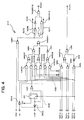
- Fig. 4 is a logic circuit diagram of the multiplexer 214 shown in Fig. 3.
- the oscillating output XCICL from the oscillating circuit 90, the output COMP from the comparator 212, or the output from the ID setting circuit 400 is selected according to the output TSINV, TEST1S, TEST11 to TEST14, and TEST16 from the command decoder 110 shown in Fig. 3, and the output TSTOUT of the multiplexer 214 is obtained.
- the multiplexer 214 has inverters INV1 to INV5, NAND gates NAND1 to NAND13, NOR gates NOR1 to NOR8, and a D-type flip-flop DFF.
- the inverter INV2, D-type flip-flop DFF, and NOR gate NOR1 function as a circuit 216 that latches the fail status when the output of the comparator 212 is LOW.
- LOW is output during the inspection at the inspection circuit 200 and HIGH is output at any other time.
- the signal TEST1S shown in Fig. 4 is held HIGH only when monitoring the output of the oscillation circuit 90.
- the signal TEST16 is held HIGH only when monitoring voltages according to the output of the comparator 212.
- the signals TEST11 to TEST14 are held HIGH in turn one after another when monitoring the ID from the ID setting circuit 400.
- the signal TSINV shown in Fig. 4 is used for switching so that the output signal at the node "a” shown in Fig. 4 is output through either one of the non-inverting output path OUT1 or the inverting output path OUT2 as shown in Fig. 4.
- the output signal at node "a” passes through the non-inverting output path OUT1
- the logic is output without changing; and when the output signal at node "a” passes through the inverting output path OUT2, the inverted logic is output.
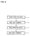
- the method of inspecting whether the oscillation circuit 90 of the liquid crystal display drive IC 90 is normal or not normal is described by referring to the flowchart in Fig. 5 and the timing diagram in Fig. 6.
- the MPU 300 cancels the power save mode of the liquid crystal display driver IC 10 (Step 1 in Fig. 5). This step is performed to operate the oscillation circuit 90 in the normal mode, not in the power save mode.
- the MPU 300 outputs the test command for monitoring the output of the oscillation circuit 90 by the MPU 300 (Step 2 in Fig. 5).
- the 8-bit test command is output being synchronized with eight pulses of the serial clock SCL of as shown in Fig. 6, and input serially to the liquid crystal display driver IC 10 via the first input-output terminal 101.
- This test command is input serially to the shift register 109 through the second transmission gate 114 shown in Fig. 3.
- the shift register 109 shifts the serial data according to the serial clock signal (SCL) which is input via the second input terminal 102, and outputs the 8-bit test command D0 to D8 in parallel.
- This test command is decoded by the command decoder 110.
- the multiplexer 214 is controlled so as to select and output the output from the oscillation circuit 90.
- the signal TEST1S alone goes HIGH, and the other signals are LOW during the monitoring process of the oscillation circuit output.
- the logic of the output XICL of the oscillation circuit 90 is inverted by each of the inverter INV1, NAND gate NAND1, NOR gate NOR7, NOR gate NOR15, and NAND gate NAND11, and consequently the inverted output of the output XICL of the oscillation circuit 90 is obtained at the node "a".
- the signals TSINV and TEST1S input to the NOR gate NOR7 are LOW and HIGH, respectively, and hence the output of the NOR gate NOR7 is set LOW.
- the inverting output path OUT2 in Fig. 3 is selected for the output path after the node "a".
- the autoreturn circuit 111 in Fig. 3 counts eight pulses of the serial clock signal (SCL) when the 8-bit test command is input, whereby the second transmission gate 114 is turned off and the first transmission gate 112 is turned on.
- the output of the oscillation circuit 90 selected as the output of the multiplexer 214 is output to the external MPU 300 via the first input-output terminal 101.
- the oscillation circuit 90 is oscillating in the normal mode because the power save mode is canceled.
- the MPU 300 is set in the oscillation output read status (Step 3 in Fig. 5) and measures the oscillation frequency of the oscillation circuit 90.
- the MPU 300 stops the generation of the serial clock signal (SCL).
- the oscillation output is of a low frequency, for example, several ten kilohertz, whereas the serial clock signal (SCL) is of a high frequency, for example, 4 MHz. Therefore, measuring the low-frequency oscillation output to the timing of the serial clock signal (SCL) only results in many times of measurements of the state of the oscillation output without change. For this reason, the oscillation frequency is measured by stopping the serial clock signal (SCL) and reading the change in the level of the oscillation output to a constant timing suited to the oscillation frequency or by using an event counter.
- the MPU 300 After this measurement is completed, the MPU 300 outputs eight serial clock pluses (SCL) as shown in Fig. 6.
- SCL serial clock pluses
- Significance of this monitoring of the oscillation output of the oscillation circuit 90 resides in that, since the oscillation circuit 90 operates on the logic voltage supply from the logic voltage input section 54, the operator can know that the normal logic voltages are supplied to the logic voltage input section 54 if the oscillation output is normal. This indicates that the contact of the elastic connection material 40 of the power IC310 and the logic voltage input section 54 is normal.
- first input-output terminal 101 and the second input terminal 102 are also maintained in normal contact based on the fact that the command data from the MPU 300 and the oscillation output data from the liquid crystal display driver IC 10 can be normally input or output.
- the ID monitoring process is preferably performed following the oscillation output monitoring process described above when the result of the inspection is normal, it may also be performed at another timing.
- the one input terminal of the NAND gate 6 is connected to voltage VDD and one input terminal of each of the other NAND gates 3 to 5 is connected to potential VSS in order to set a particular ID for the liquid crystal display driver IC 10.
- 2 4 16 IDs can be set by changing the wiring.
- the test command is input from the MPU 300 to the liquid crystal display driver IC 10.
- the signals TEST11 to TEST14 to the other input terminals of the aforementioned NAND gates NAND3 to NAND6 are brought HIGH selectively one after another in the order from TEST14 to TEST11.
- signal TSINV is held LOW in the first half period during which the outputs of the NAND gates NAND3 to NAND6 are read out, and held HIGH in the second half period.
- the other signals TEST1S and TEST16 shown in Fig. 4 are held LOW.
- ID1 to ID4 each consisting of 8 bits, shown in Table 1 below are read out one by one, and IDs of 32 bits in total are monitored by the MPU 300.
- Type of ID ID Read High Significant Bits Non-inverted Low Significant Bits Inverted D7 D6 D5 D4 D3 D2 D1 D0 ID1 NAND6 1 1 1 1 0 0 0 0 ID2 NANDS 0 0 0 0 1 1 1 1 ID3 NAND4 0 0 0 0 1 1 1 1 ID4 NAND3 0 0 0 0 1 1 1 1 1 1 1 1 1 1 1 1 1 1 1 1 1 1 1 1 1 1 1 1 1 1 1 1 1 1 1 1 1 1 1 1 1 1 1 1 1 1 1 1 1 1 1 1 1 1 1 1 1 1 1 1 1 1 1 1 1 1 1 1 1 1 1 1 1 1 1 1 1 1 1 1 1 1 1 1 1 1 1 1 1 1 1 1 1 1 1 1 1 1 1 1 1 1 1 1 1 1 1 1 1 1 1 1 1 1 1 1 1
- test command for reading out the ID is decoded by the command decoder 110 via the input-output terminal 101, the second transmission gate 114, and the shift register 109 in the same manner as described above.
- the multiplexer 214 is thereby controlled so as to select the output of the ID setting circuit 400 and output it.
- TEST11 is first brought to HIGH, and TEST12 to TEST14 are held LOW by this test command.
- the signal TSINV is held LOW at first. Consequently, one input voltage VDD (HIGH) is inverted by each of the NAND gate NAND9, inverter INV4, and NAND gate NAND11, and hence HIGH is obtained at the node "a".
- VDD high input voltage
- the non-inverting output path OUT1 is selected, and the logic HIGH at the node "a” is obtained as is as the output TSTOUT of the multiplexer 214.
- This output of the multiplexer 214 is output by the MPU interface 100 in accordance with the serial clock signal CLK, that is, the status of each of the high significant four bits D7 to D4 is output as "1" as shown in the above Table 1 and Fig. 8.
- the signal TSINV is switched from LOW to HIGH as shown in Fig. 8.
- the output of the NAND gate NAND7 is thereby fixed to LOW, and the inverting output path OUT2 is selected.
- the logic HIGH at the node "a” is thereby inverted, and LOW is obtained as the output TSTOUT of the multiplexer 214.
- This output of the multiplexer 214 is also output by the MPU interface 100 in accordance with the serial clock signal CLK, that is, the status of each of the low significant four bits D3 to D0 is output as "0" as shown in the above Table 1 and Fig. 8.
- non-inverted high significant four bits and inverted low significant four bits are obtained as ID2 to ID4 shown in Table 1 by bringing the signals TEST12, TEST13, and TEST14 HIGH one by one.
- ID1 to ID4 32 bits in total, shown in Table 1 are thus input to the MPU 300, and the MPU 300 reads the ID (Step 2 in Fig. 7). If the eight bits of each of ID1 to ID4 having been input to the MPU 300 have the low significant four bits inverted against the logic of the high significant four bits, the connection of the logic power supply and that of the serial interface can be judged to be normal. This is because the eight bits of each of ID1 to ID4 do not have the non-inverted and inverted logic states by four bits if there is any abnormality in these connections.
- a parity check is generally performed to check whether serial data is being transferred normally.
- the number of data "1"s is checked using an adder.
- an adder occupies a substantial area in the IC because of possession of a large circuit size. This embodiment makes it possible to judge whether the serial interface is normal without need of such a large circuit.
- the MPU 300 sends the reset command, whereby the ID monitoring process terminates (Step 3 in Fig. 7).
- this voltage monitoring process is preferably performed following the ID monitoring process described above when the result of the inspection is normal, it may also be performed at any other timing.
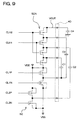
- Fig. 9 shows the booster circuit 52 and its external booster capacitors C1 to C4.
- Fig. 10 shows waveforms of the booster clock signal for driving the booster transistors shown in Fig. 9.
- the booster capacitors C1 to C4 are connected to the group of booster transistors 52A via the elastic-connecting member 40.
- the booster clock signals CLH1, CLH2, CL1P, CL2P, CL1N, and CL2N are applied to the gates of the booster transistors 52A at the timing shown in Fig. 10. These booster clock signals are generated by dividing the output of the oscillation circuit 90. Therefore, this voltage-monitoring process may be preferably performed after the oscillation output of the oscillation circuit 90 has been decided to be normal.
- VDD2 (2.7 V, for example) and 2 ⁇ VDD2 are alternately charged to the booster capacitor C1
- voltages of 2VDD2 and 4 ⁇ VDD2 are alternately charged to the booster capacitor C2
- voltages of 3 ⁇ VDD2 and 4 ⁇ VDD2 are alternately charged to the booster capacitor C3.
- the above-described operation requires connection between the booster transistors 52A and the booster capacitors C1 to C4 via the elastic-connecting member 40 without an inadequate contact. If there is no problem with the connection, the output voltage VOUT of the booster circuit 52 is maintained constant as shown in Fig. 11. However, if the connection of the booster capacitor C1 is faulty, for example, the output voltage VOUT varies in synchronism with the booster clock as shown in Fig. 12. Ripples appear in the waveform of the output voltage when the connection is abnormal, and the peaks of the ripples are about the same values as the normal value shown in Fig. 11.
- the output voltage VOUT of the booster circuit 52 is monitored.
- the voltage VOUT is divided by the voltage monitoring circuit 210 by resistance division and input to one input terminal of the comparator 212.
- a reference voltage 1.5 V, for example
- the output voltage VOUT is divided so that the output voltage VOUT of the booster circuit 52 is a little higher than the reference voltage when the output voltage VOUT is normal. Therefore, if the output voltage of the voltage-monitoring circuit 210 is higher than the reference voltage, the output of the comparator 212 is HIGH, indicating that the output voltage VOUT is normal. If one or more of the booster capacitors are out of connection, on the other hand, the waveform as shown in Fig. 12 is generated, whereby the output voltage of the comparator 212 is not always HIGH, but can go LOW.
- the power save mode is canceled (Step 1 in Fig. 13), and the oscillation circuit 90 is driven in the normal mode.
- the booster circuit 52 is then turned on (Step 2 in Fig. 13), and a waiting time is allowed until the booster capacitor C4 is charged to voltage 4 ⁇ VDD2 (Step 3 in Fig. 13).
- test command is also decoded by the command decoder 110 in the same manner as described above.
- signal TEST16 shown in Fig. 4 alone goes HIGH, and the other test signals TSINV, TEST1S, and TEST11 to TEST14 are all LOW.
- the non-inverting output path OUT1 is selected.
- the logic (HIGH) at the node “a” is therefore output as is as the output TSTOUT of the multiplexer 214 via the NAND gate NAND12 and NAND gate NAND13.
- the output signal of the multiplexer 214 is also output via the MPU interface 100 to the serial clock signal CLK. This is performed during one period H of the boosting operation or longer time (Step 5 in Fig. 13).
- the output of the multiplexer 214 is read by the MPU 300 (Step 6 in Fig. 13), and the output voltage VOUT of the booster circuit 52 is judged to be normal if the output logic of the multiplexer 214 is HIGH.
- Step 5 in Fig. 13 the voltage is monitored for at least one period H of the booster clock, and any abnormality in the output voltage VOUT can be latched by the fail status latch circuit 216 shown in Fig. 4.
- the logic (LOW) at the node “a” shown in Fig. 4 is output as is as the output TSTOUT of the multiplexer 214 via the NAND gates NAND12 and NAND13.
- the MPU 300 to which this is input, can judge that the output voltage VOUT of the booster circuit 52 is abnormal when the logic is LOW by reading the output of the multiplexer 214 (Step 6 in Fig. 13) after the waiting time in Step 5 in Fig. 13.
- the MPU 300 then sends the reset command, and the voltage monitoring process terminates (Step 7 in Fig. 13).
- the MPU 300 can be configured so that it can be used with two or more types of liquid crystal display driver ICs.
- the MPU 300 has two or more sets of display control contents for two or more liquid crystal display driver ICs stored in a storage section, for example, PROM (Programmable Read Only Memory) in correspondence to a plurality of IDs.
- PROM Programmable Read Only Memory
- liquid crystal display driver ICs used with the same MPU 300
- the following types A and B used for driving liquid crystal panels of different display capacities can be given.
- An ID that is set by the ID setting circuit 400 of the liquid crystal driver IC 10 can be used not only for the inspection process described above but also for selecting one set of control contents among those for a plurality of types of driver ICs stored in the storage section of the MPU 300 as described below.
- the reading of the ID from the liquid crystal display driver IC 10 can be performed every time a device with this IC mounted therein is switched on or after every power-on reset.
- the ID read command is sent from the MPU 300 in this timing, the ID from the liquid crystal display driver IC 10 is read by the MPU 300 in the same manner as in the ID monitoring process.
- the ID reading method is standardized among venders and types.
- the ID read is stored in a register or memory, for example, RAM in the device. If the memory is nonvolatile, the ID that is read in the above-described inspection process at the factory can be stored. Thus, reading and storing of the ID every time the device is switched on or after every power-on reset becomes unnecessary.
- Control contents which correspond the ID stored in a memory, are then selected according to the stored ID, and the liquid crystal display driver IC 10 can be controlled using the control contents.
- control contents corresponding to the ID are selected and stored in the RAM by referring to a look-up table in the ROM according to the ID stored in the RAM, for example.
- the information in the control contents includes, for example, the screen size and display capacity of the liquid crystal panel and various commands (address set, display ON/OFF, etc.).
- the present invention is not limited to the embodiments described above, and various modifications may be made within the sprits and scope of the present invention.
- the present invention can also be applied to a configuration which allows the user to switch input of data such as command data and display data between serial and parallel, because the operation by the configuration of the present invention can be performed at least when serial input is used.
- the display driver IC of the present invention can be used not only for liquid crystal displays but also for other various types of displays.
- An electronic device of the present invention is also not limited to a cellular phone, and can be applied to other various electronic devices of which the liquid crystal or the other type of display unit is driven according to the data input serially.
Landscapes
- Engineering & Computer Science (AREA)
- Theoretical Computer Science (AREA)
- Physics & Mathematics (AREA)
- General Physics & Mathematics (AREA)
- Computer Hardware Design (AREA)
- General Engineering & Computer Science (AREA)
- Quality & Reliability (AREA)
- Crystallography & Structural Chemistry (AREA)
- Chemical & Material Sciences (AREA)
- Control Of Indicators Other Than Cathode Ray Tubes (AREA)
- Liquid Crystal Display Device Control (AREA)
- Devices For Indicating Variable Information By Combining Individual Elements (AREA)
- Testing Of Short-Circuits, Discontinuities, Leakage, Or Incorrect Line Connections (AREA)
- Testing Electric Properties And Detecting Electric Faults (AREA)
- Stored Programmes (AREA)
- Selective Calling Equipment (AREA)
Priority Applications (1)
| Application Number | Priority Date | Filing Date | Title |
|---|---|---|---|
| EP08014982A EP1988540A3 (de) | 1999-08-12 | 2000-08-09 | Treiber |
Applications Claiming Priority (3)
| Application Number | Priority Date | Filing Date | Title |
|---|---|---|---|
| JP22838999 | 1999-08-12 | ||
| JP22838999A JP3815131B2 (ja) | 1999-08-12 | 1999-08-12 | 表示ユニット及びそれを用いた電子機器並びに表示ユニットの検査方法 |
| EP00117083A EP1076292B1 (de) | 1999-08-12 | 2000-08-09 | Anzeigeeinheit, selbige verwendendes elektronisches Gerät, und Verfahren zur Inspektion der Anzeigeeinheit |
Related Parent Applications (1)
| Application Number | Title | Priority Date | Filing Date |
|---|---|---|---|
| EP00117083A Division EP1076292B1 (de) | 1999-08-12 | 2000-08-09 | Anzeigeeinheit, selbige verwendendes elektronisches Gerät, und Verfahren zur Inspektion der Anzeigeeinheit |
Related Child Applications (1)
| Application Number | Title | Priority Date | Filing Date |
|---|---|---|---|
| EP08014982A Division EP1988540A3 (de) | 1999-08-12 | 2000-08-09 | Treiber |
Publications (3)
| Publication Number | Publication Date |
|---|---|
| EP1320084A2 true EP1320084A2 (de) | 2003-06-18 |
| EP1320084A3 EP1320084A3 (de) | 2004-05-26 |
| EP1320084B1 EP1320084B1 (de) | 2008-11-05 |
Family
ID=16875713
Family Applications (3)
| Application Number | Title | Priority Date | Filing Date |
|---|---|---|---|
| EP03000508A Expired - Lifetime EP1320084B1 (de) | 1999-08-12 | 2000-08-09 | Anzeigevorrichtung und elektronisches Gerät und Vorrichtung hierfür |
| EP08014982A Withdrawn EP1988540A3 (de) | 1999-08-12 | 2000-08-09 | Treiber |
| EP00117083A Expired - Lifetime EP1076292B1 (de) | 1999-08-12 | 2000-08-09 | Anzeigeeinheit, selbige verwendendes elektronisches Gerät, und Verfahren zur Inspektion der Anzeigeeinheit |
Family Applications After (2)
| Application Number | Title | Priority Date | Filing Date |
|---|---|---|---|
| EP08014982A Withdrawn EP1988540A3 (de) | 1999-08-12 | 2000-08-09 | Treiber |
| EP00117083A Expired - Lifetime EP1076292B1 (de) | 1999-08-12 | 2000-08-09 | Anzeigeeinheit, selbige verwendendes elektronisches Gerät, und Verfahren zur Inspektion der Anzeigeeinheit |
Country Status (6)
| Country | Link |
|---|---|
| US (3) | US6657648B1 (de) |
| EP (3) | EP1320084B1 (de) |
| JP (1) | JP3815131B2 (de) |
| KR (1) | KR100380258B1 (de) |
| CN (1) | CN1163043C (de) |
| DE (2) | DE60040761D1 (de) |
Cited By (1)
| Publication number | Priority date | Publication date | Assignee | Title |
|---|---|---|---|---|
| EP2099015A3 (de) * | 2008-03-05 | 2011-04-06 | Samsung Electronics Co., Ltd. | Vorrichtung und Verfahren zur Unterscheidung eines Paneels einer Anzeige |
Families Citing this family (19)
| Publication number | Priority date | Publication date | Assignee | Title |
|---|---|---|---|---|
| JP3736622B2 (ja) * | 2001-06-15 | 2006-01-18 | セイコーエプソン株式会社 | ライン駆動回路、電気光学装置及び表示装置 |
| JP2004021067A (ja) * | 2002-06-19 | 2004-01-22 | Sanyo Electric Co Ltd | 液晶表示装置、液晶表示装置の調整方法 |
| JP4055572B2 (ja) * | 2002-12-24 | 2008-03-05 | セイコーエプソン株式会社 | 表示システム及び表示コントローラ |
| US7573286B2 (en) * | 2003-05-16 | 2009-08-11 | E.I. Du Pont De Nemours And Company | System and method for testing displays |
| JP4016915B2 (ja) * | 2003-09-11 | 2007-12-05 | 株式会社日立製作所 | 表示システム及びそれに用いられる表示パネル、信号処理装置 |
| US20060017715A1 (en) * | 2004-04-14 | 2006-01-26 | Pioneer Plasm Display Corporation | Display device, display driver, and data transfer method |
| TWI275055B (en) * | 2004-11-26 | 2007-03-01 | Hon Hai Prec Ind Co Ltd | System and method for sharing MCU codes |
| US7519863B2 (en) * | 2005-05-20 | 2009-04-14 | Nokia Corporation | Detection of a malfunction in a hardware module |
| KR101189278B1 (ko) * | 2006-04-18 | 2012-10-09 | 삼성디스플레이 주식회사 | 디지털 아날로그 변환기 및 표시 장치의 구동 방법 |
| JP2008294381A (ja) * | 2007-05-28 | 2008-12-04 | Panasonic Corp | 電子部品モジュール及び電子部品モジュールの製造方法 |
| JP2009204558A (ja) * | 2008-02-29 | 2009-09-10 | Keihin Corp | バックアップコンデンサの容量診断方法 |
| JP5465918B2 (ja) * | 2009-05-13 | 2014-04-09 | 矢崎総業株式会社 | ノイズ対策構造 |
| CN101996560B (zh) * | 2010-11-05 | 2014-08-06 | 彩优微电子(昆山)有限公司 | 一种显示驱动装置以及显示驱动方法 |
| CN102945648B (zh) * | 2012-11-26 | 2015-03-25 | 京东方科技集团股份有限公司 | 一种显示装置的测试设备及测试方法 |
| CN103236242A (zh) * | 2013-04-23 | 2013-08-07 | 青岛海信电器股份有限公司 | 一种显示面板测试用信号产生装置 |
| CN104597366B (zh) * | 2014-12-31 | 2017-10-31 | 孙厚永 | 一种测试房的测试工装 |
| KR102448373B1 (ko) * | 2015-06-15 | 2022-09-29 | 삼성디스플레이 주식회사 | 표시장치 및 표시장치 구동방법 |
| US10643511B2 (en) * | 2016-08-19 | 2020-05-05 | Apple Inc. | Electronic device display with monitoring circuitry |
| TWI682182B (zh) * | 2019-03-07 | 2020-01-11 | 緯創資通股份有限公司 | 檢測設備及其檢測方法 |
Family Cites Families (23)
| Publication number | Priority date | Publication date | Assignee | Title |
|---|---|---|---|---|
| JPH0743581B2 (ja) * | 1990-10-31 | 1995-05-15 | ヤマハ株式会社 | ディスプレイ制御装置 |
| US5081687A (en) * | 1990-11-30 | 1992-01-14 | Photon Dynamics, Inc. | Method and apparatus for testing LCD panel array prior to shorting bar removal |
| JPH04276792A (ja) | 1991-03-05 | 1992-10-01 | Nec Corp | 集合型表示装置 |
| US5670969A (en) * | 1991-10-14 | 1997-09-23 | Hitachi, Ltd. | Information processing apparatus |
| JP3084114B2 (ja) * | 1992-01-06 | 2000-09-04 | パイオニア株式会社 | カーステレオ |
| JP2935307B2 (ja) * | 1992-02-20 | 1999-08-16 | 株式会社日立製作所 | ディスプレイ |
| US5262759A (en) * | 1992-07-27 | 1993-11-16 | Cordata Incorporated | Removable computer display interface |
| JPH07146665A (ja) | 1993-09-30 | 1995-06-06 | Toshiba Lighting & Technol Corp | 表示制御監視装置 |
| JPH07175454A (ja) * | 1993-10-25 | 1995-07-14 | Toshiba Corp | 表示制御装置および表示制御方法 |
| JP3159586B2 (ja) | 1993-12-09 | 2001-04-23 | 株式会社東芝 | 昇圧回路装置 |
| US5565897A (en) * | 1994-01-14 | 1996-10-15 | Elonex Technologies, Inc. | Interactive system for calibration of display monitors |
| JP2765576B2 (ja) | 1994-01-17 | 1998-06-18 | セイコーエプソン株式会社 | 電子時計 |
| JPH07260857A (ja) | 1994-03-18 | 1995-10-13 | Fujitsu Ltd | 液晶表示装置の駆動回路および液晶表示装置 |
| US5440339A (en) * | 1994-04-13 | 1995-08-08 | U.S. Philips Corporation | System and method for testing intensity response of a medical monochrome video monitor |
| US5499040A (en) * | 1994-06-27 | 1996-03-12 | Radius Inc. | Method and apparatus for display calibration and control |
| JPH08223514A (ja) | 1995-02-20 | 1996-08-30 | Fujitsu General Ltd | マルチパネルシステム |
| JPH09114428A (ja) * | 1995-10-19 | 1997-05-02 | Hitachi Ltd | 情報処理装置 |
| JP3627408B2 (ja) | 1996-10-23 | 2005-03-09 | セイコーエプソン株式会社 | 表示体の駆動回路,半導体集積回路装置,表示装置および電子機器 |
| JP3907131B2 (ja) * | 1997-01-27 | 2007-04-18 | コーニンクレッカ フィリップス エレクトロニクス エヌ ヴィ | 液晶表示装置を製造する方法 |
| JPH10268834A (ja) | 1997-03-21 | 1998-10-09 | Mitsubishi Electric Corp | 集合型表示装置 |
| JPH10312172A (ja) | 1997-05-13 | 1998-11-24 | Sony Corp | 表示回路 |
| JPH10323154A (ja) * | 1997-05-26 | 1998-12-08 | Watanabe Seihou | 無塩梅漬けの製法 |
| JP3582382B2 (ja) * | 1998-11-13 | 2004-10-27 | 株式会社日立製作所 | マルチディスプレイ装置の表示制御装置、表示装置及びマルチディスプレイ装置 |
-
1999
- 1999-08-12 JP JP22838999A patent/JP3815131B2/ja not_active Expired - Fee Related
-
2000
- 2000-08-07 US US09/634,876 patent/US6657648B1/en not_active Expired - Fee Related
- 2000-08-09 EP EP03000508A patent/EP1320084B1/de not_active Expired - Lifetime
- 2000-08-09 DE DE60040761T patent/DE60040761D1/de not_active Expired - Lifetime
- 2000-08-09 DE DE60016678T patent/DE60016678T2/de not_active Expired - Lifetime
- 2000-08-09 EP EP08014982A patent/EP1988540A3/de not_active Withdrawn
- 2000-08-09 EP EP00117083A patent/EP1076292B1/de not_active Expired - Lifetime
- 2000-08-11 KR KR10-2000-0046543A patent/KR100380258B1/ko not_active Expired - Fee Related
- 2000-08-14 CN CNB001227807A patent/CN1163043C/zh not_active Expired - Fee Related
-
2003
- 2003-10-02 US US10/676,149 patent/US7129936B2/en not_active Ceased
-
2008
- 2008-10-30 US US12/289,617 patent/USRE42569E1/en not_active Expired - Fee Related
Cited By (2)
| Publication number | Priority date | Publication date | Assignee | Title |
|---|---|---|---|---|
| EP2099015A3 (de) * | 2008-03-05 | 2011-04-06 | Samsung Electronics Co., Ltd. | Vorrichtung und Verfahren zur Unterscheidung eines Paneels einer Anzeige |
| US8194024B2 (en) | 2008-03-05 | 2012-06-05 | Samsung Electronics Co., Ltd. | Apparatus and method for distinguishing panel of display device |
Also Published As
| Publication number | Publication date |
|---|---|
| EP1076292B1 (de) | 2004-12-15 |
| EP1320084A3 (de) | 2004-05-26 |
| DE60016678D1 (de) | 2005-01-20 |
| EP1076292A2 (de) | 2001-02-14 |
| EP1988540A2 (de) | 2008-11-05 |
| CN1163043C (zh) | 2004-08-18 |
| USRE42569E1 (en) | 2011-07-26 |
| JP3815131B2 (ja) | 2006-08-30 |
| KR20010021274A (ko) | 2001-03-15 |
| CN1284808A (zh) | 2001-02-21 |
| EP1076292A3 (de) | 2002-01-02 |
| US7129936B2 (en) | 2006-10-31 |
| EP1988540A3 (de) | 2009-01-14 |
| JP2001051644A (ja) | 2001-02-23 |
| DE60040761D1 (de) | 2008-12-18 |
| KR100380258B1 (ko) | 2003-04-16 |
| US20040066382A1 (en) | 2004-04-08 |
| DE60016678T2 (de) | 2005-10-06 |
| EP1320084B1 (de) | 2008-11-05 |
| US6657648B1 (en) | 2003-12-02 |
Similar Documents
| Publication | Publication Date | Title |
|---|---|---|
| USRE42569E1 (en) | Display unit, electronic device using the same, and method of inspecting the display unit | |
| US20090158093A1 (en) | Motherboard tester | |
| CN216287519U (zh) | 一种驱动芯片测试电路及系统 | |
| US6130657A (en) | Liquid crystal display device | |
| CN107340415A (zh) | 一种信号补偿器及其信号补偿方法、信号补偿系统 | |
| US10872576B2 (en) | Display driver IC | |
| US6473059B1 (en) | Display driver IC and electronic device using same | |
| CN101894057B (zh) | 主板故障诊断卡 | |
| US20050122297A1 (en) | Semiconductor device and the method of testing the same | |
| US5065356A (en) | Shared use of keyboard and memory lines | |
| CN1110095C (zh) | 半导体装置及半导体装置的内部功能识别方法 | |
| CN216162802U (zh) | 一种信号时序测试转接板 | |
| CN117456894A (zh) | 显示驱动装置及其驱动器的测试方法 | |
| US20070075126A1 (en) | Identification method and system | |
| CN100419446C (zh) | 半导体器件及其测试方法 | |
| CN1979269A (zh) | 液晶显示面板 | |
| CN119007674B (zh) | 印刷电路板组件、显示模组、显示装置和显示控制方法 | |
| US6034880A (en) | Embedded memory device and method of performing a burn-in process on the embedded memory device | |
| CN221200764U (zh) | 一种测试设备 | |
| CN110491332A (zh) | 驱动器、显示装置及其使用方法 | |
| CN109345991A (zh) | 显示驱动方法、显示驱动装置和显示装置 | |
| CN121747440A (zh) | 显示驱动器和显示装置 | |
| CN1414423A (zh) | 平面显示器面板 | |
| CN118942362A (zh) | 一种多屏兼容的主板 | |
| TWI442411B (zh) | 讀寫保護電路 |
Legal Events
| Date | Code | Title | Description |
|---|---|---|---|
| PUAI | Public reference made under article 153(3) epc to a published international application that has entered the european phase |
Free format text: ORIGINAL CODE: 0009012 |
|
| AC | Divisional application: reference to earlier application |
Ref document number: 1076292 Country of ref document: EP Kind code of ref document: P |
|
| AK | Designated contracting states |
Designated state(s): DE FI FR NL |
|
| PUAL | Search report despatched |
Free format text: ORIGINAL CODE: 0009013 |
|
| AK | Designated contracting states |
Kind code of ref document: A3 Designated state(s): DE FI FR NL |
|
| 17P | Request for examination filed |
Effective date: 20040923 |
|
| AKX | Designation fees paid |
Designated state(s): DE FI FR NL |
|
| 17Q | First examination report despatched |
Effective date: 20050613 |
|
| 17Q | First examination report despatched |
Effective date: 20050613 |
|
| GRAP | Despatch of communication of intention to grant a patent |
Free format text: ORIGINAL CODE: EPIDOSNIGR1 |
|
| GRAS | Grant fee paid |
Free format text: ORIGINAL CODE: EPIDOSNIGR3 |
|
| GRAA | (expected) grant |
Free format text: ORIGINAL CODE: 0009210 |
|
| AC | Divisional application: reference to earlier application |
Ref document number: 1076292 Country of ref document: EP Kind code of ref document: P |
|
| AK | Designated contracting states |
Kind code of ref document: B1 Designated state(s): DE FI FR NL |
|
| REF | Corresponds to: |
Ref document number: 60040761 Country of ref document: DE Date of ref document: 20081218 Kind code of ref document: P |
|
| PLBE | No opposition filed within time limit |
Free format text: ORIGINAL CODE: 0009261 |
|
| STAA | Information on the status of an ep patent application or granted ep patent |
Free format text: STATUS: NO OPPOSITION FILED WITHIN TIME LIMIT |
|
| 26N | No opposition filed |
Effective date: 20090806 |
|
| PGFP | Annual fee paid to national office [announced via postgrant information from national office to epo] |
Ref country code: DE Payment date: 20140806 Year of fee payment: 15 Ref country code: NL Payment date: 20140710 Year of fee payment: 15 Ref country code: FI Payment date: 20140812 Year of fee payment: 15 |
|
| PGFP | Annual fee paid to national office [announced via postgrant information from national office to epo] |
Ref country code: FR Payment date: 20140808 Year of fee payment: 15 |
|
| REG | Reference to a national code |
Ref country code: DE Ref legal event code: R119 Ref document number: 60040761 Country of ref document: DE |
|
| REG | Reference to a national code |
Ref country code: NL Ref legal event code: MM Effective date: 20150901 |
|
| PG25 | Lapsed in a contracting state [announced via postgrant information from national office to epo] |
Ref country code: FI Free format text: LAPSE BECAUSE OF NON-PAYMENT OF DUE FEES Effective date: 20150809 |
|
| REG | Reference to a national code |
Ref country code: FR Ref legal event code: ST Effective date: 20160429 |
|
| PG25 | Lapsed in a contracting state [announced via postgrant information from national office to epo] |
Ref country code: NL Free format text: LAPSE BECAUSE OF NON-PAYMENT OF DUE FEES Effective date: 20150901 |
|
| PG25 | Lapsed in a contracting state [announced via postgrant information from national office to epo] |
Ref country code: DE Free format text: LAPSE BECAUSE OF NON-PAYMENT OF DUE FEES Effective date: 20160301 |
|
| PG25 | Lapsed in a contracting state [announced via postgrant information from national office to epo] |
Ref country code: FR Free format text: LAPSE BECAUSE OF NON-PAYMENT OF DUE FEES Effective date: 20150831 |