EP1320288A2 - Dispositif de panneau à circuit imprimé et son procédé de fabrication - Google Patents
Dispositif de panneau à circuit imprimé et son procédé de fabrication Download PDFInfo
- Publication number
- EP1320288A2 EP1320288A2 EP02255035A EP02255035A EP1320288A2 EP 1320288 A2 EP1320288 A2 EP 1320288A2 EP 02255035 A EP02255035 A EP 02255035A EP 02255035 A EP02255035 A EP 02255035A EP 1320288 A2 EP1320288 A2 EP 1320288A2
- Authority
- EP
- European Patent Office
- Prior art keywords
- wiring board
- parts
- circuit
- printed wiring
- heat
- Prior art date
- Legal status (The legal status is an assumption and is not a legal conclusion. Google has not performed a legal analysis and makes no representation as to the accuracy of the status listed.)
- Granted
Links
Images


Classifications
-
- H—ELECTRICITY
- H05—ELECTRIC TECHNIQUES NOT OTHERWISE PROVIDED FOR
- H05K—PRINTED CIRCUITS; CASINGS OR CONSTRUCTIONAL DETAILS OF ELECTRIC APPARATUS; MANUFACTURE OF ASSEMBLAGES OF ELECTRICAL COMPONENTS
- H05K1/00—Printed circuits
- H05K1/02—Details
- H05K1/0201—Thermal arrangements, e.g. for cooling, heating or preventing overheating
- H05K1/0203—Cooling of mounted components
- H05K1/0209—External configuration of printed circuit board adapted for heat dissipation, e.g. lay-out of conductors, coatings
-
- H—ELECTRICITY
- H05—ELECTRIC TECHNIQUES NOT OTHERWISE PROVIDED FOR
- H05K—PRINTED CIRCUITS; CASINGS OR CONSTRUCTIONAL DETAILS OF ELECTRIC APPARATUS; MANUFACTURE OF ASSEMBLAGES OF ELECTRICAL COMPONENTS
- H05K1/00—Printed circuits
- H05K1/02—Details
- H05K1/0201—Thermal arrangements, e.g. for cooling, heating or preventing overheating
-
- H—ELECTRICITY
- H05—ELECTRIC TECHNIQUES NOT OTHERWISE PROVIDED FOR
- H05K—PRINTED CIRCUITS; CASINGS OR CONSTRUCTIONAL DETAILS OF ELECTRIC APPARATUS; MANUFACTURE OF ASSEMBLAGES OF ELECTRICAL COMPONENTS
- H05K3/00—Apparatus or processes for manufacturing printed circuits
- H05K3/30—Assembling printed circuits with electric components, e.g. with resistors
- H05K3/32—Assembling printed circuits with electric components, e.g. with resistors electrically connecting electric components or wires to printed circuits
- H05K3/34—Assembling printed circuits with electric components, e.g. with resistors electrically connecting electric components or wires to printed circuits by soldering
- H05K3/3494—Heating processes for reflow soldering
-
- H—ELECTRICITY
- H05—ELECTRIC TECHNIQUES NOT OTHERWISE PROVIDED FOR
- H05K—PRINTED CIRCUITS; CASINGS OR CONSTRUCTIONAL DETAILS OF ELECTRIC APPARATUS; MANUFACTURE OF ASSEMBLAGES OF ELECTRICAL COMPONENTS
- H05K2201/00—Indexing scheme relating to printed circuits covered by H05K1/00
- H05K2201/06—Thermal details
- H05K2201/066—Heatsink mounted on the surface of the printed circuit board [PCB]
-
- H—ELECTRICITY
- H05—ELECTRIC TECHNIQUES NOT OTHERWISE PROVIDED FOR
- H05K—PRINTED CIRCUITS; CASINGS OR CONSTRUCTIONAL DETAILS OF ELECTRIC APPARATUS; MANUFACTURE OF ASSEMBLAGES OF ELECTRICAL COMPONENTS
- H05K2201/00—Indexing scheme relating to printed circuits covered by H05K1/00
- H05K2201/09—Shape and layout
- H05K2201/09209—Shape and layout details of conductors
- H05K2201/09654—Shape and layout details of conductors covering at least two types of conductors provided for in H05K2201/09218 - H05K2201/095
- H05K2201/09781—Dummy conductors, i.e. not used for normal transport of current; Dummy electrodes of components
-
- H—ELECTRICITY
- H05—ELECTRIC TECHNIQUES NOT OTHERWISE PROVIDED FOR
- H05K—PRINTED CIRCUITS; CASINGS OR CONSTRUCTIONAL DETAILS OF ELECTRIC APPARATUS; MANUFACTURE OF ASSEMBLAGES OF ELECTRICAL COMPONENTS
- H05K2201/00—Indexing scheme relating to printed circuits covered by H05K1/00
- H05K2201/10—Details of components or other objects attached to or integrated in a printed circuit board
- H05K2201/10007—Types of components
- H05K2201/10204—Dummy component, dummy PCB or template, e.g. for monitoring, controlling of processes, comparing, scanning
-
- H—ELECTRICITY
- H05—ELECTRIC TECHNIQUES NOT OTHERWISE PROVIDED FOR
- H05K—PRINTED CIRCUITS; CASINGS OR CONSTRUCTIONAL DETAILS OF ELECTRIC APPARATUS; MANUFACTURE OF ASSEMBLAGES OF ELECTRICAL COMPONENTS
- H05K2203/00—Indexing scheme relating to apparatus or processes for manufacturing printed circuits covered by H05K3/00
- H05K2203/11—Treatments characterised by their effect, e.g. heating, cooling, roughening
- H05K2203/1121—Cooling, e.g. specific areas of a PCB being cooled during reflow soldering
-
- H—ELECTRICITY
- H05—ELECTRIC TECHNIQUES NOT OTHERWISE PROVIDED FOR
- H05K—PRINTED CIRCUITS; CASINGS OR CONSTRUCTIONAL DETAILS OF ELECTRIC APPARATUS; MANUFACTURE OF ASSEMBLAGES OF ELECTRICAL COMPONENTS
- H05K2203/00—Indexing scheme relating to apparatus or processes for manufacturing printed circuits covered by H05K3/00
- H05K2203/30—Details of processes not otherwise provided for in H05K2203/01 - H05K2203/17
- H05K2203/304—Protecting a component during manufacturing
-
- Y—GENERAL TAGGING OF NEW TECHNOLOGICAL DEVELOPMENTS; GENERAL TAGGING OF CROSS-SECTIONAL TECHNOLOGIES SPANNING OVER SEVERAL SECTIONS OF THE IPC; TECHNICAL SUBJECTS COVERED BY FORMER USPC CROSS-REFERENCE ART COLLECTIONS [XRACs] AND DIGESTS
- Y10—TECHNICAL SUBJECTS COVERED BY FORMER USPC
- Y10T—TECHNICAL SUBJECTS COVERED BY FORMER US CLASSIFICATION
- Y10T29/00—Metal working
- Y10T29/49—Method of mechanical manufacture
- Y10T29/49002—Electrical device making
- Y10T29/49117—Conductor or circuit manufacturing
- Y10T29/49124—On flat or curved insulated base, e.g., printed circuit, etc.
- Y10T29/4913—Assembling to base an electrical component, e.g., capacitor, etc.
- Y10T29/49144—Assembling to base an electrical component, e.g., capacitor, etc. by metal fusion
Definitions
- the present invention relates to a printed wiring board device on which solder junctions of individual parts are made by using reflow equipment, and to a method of manufacture of the printed wiring board device.
- the melting point of the unleaded solder is raised from 183 deg. C that is the melting point of the eutectic alloy solder.
- the melting point of the Sn-Zn unleaded solder goes up to 200 deg. C
- the melting point of the Sn-Ag-Cu unleaded solder goes up to 217-221 deg. C.
- the mounting temperature that ensures good solder junctions in the case of the unleaded solder is also raised by about 10-20 deg. C from 205 deg. C that is the mounting temperature in the case of the leaded solder.
- the reliability of individual parts of the printed wiring board is significantly affected.
- the heat-resistant temperature of the printed wiring board parts varies depending on the composition material and size of the individual parts. Even if the leaded solder is replaced by the unleaded solder, the heat-resistant temperature remains unchanged. Hence, it is necessary to take measures to reduce the time to maintain the high temperature conditions as small as possible for the printed wiring board parts wherein the permissible temperature conditions are severe.
- the conventional circuit parts should not be used without change. It is necessary to change the conventional circuit parts to special circuit parts using a composition material having a high thermal resistance or to improve the manufacturing processes by taking preventive measures against the peeling or swelling of the resin layer of the isolated parts.
- Japanese Laid-Open Patent Application Nos. 2001-85827, 8-64953 and 8-236913 disclose improvements of pads and circuit patterns for a printed wiring board that is configured to suppress the temperature variations of the lead portion of each individual part on the printed wiring board to obtain the uniform temperature, and to suppress irregularities of solder junctions at the time of soldering.
- Japanese Published Utility Model Application No. 7-37337 discloses an electronic circuit chip in which dummy parts are provided.
- the dummy parts are provided in order to prevent the engagement between adjacent circuit chips when arranging the circuit chips in row into a cylindrical case and mounting the circuit chips on a printed circuit board by using an automatic mounting machine.
- a conceivable method for improvement of the manufacturing processes is that a special jig is provided in order to prevent the heat concentration on specific circuit parts.
- a special jig is provided in order to prevent the heat concentration on specific circuit parts.
- An object of the present invention is to provide an improved printed wiring board device in which the above-described problems are eliminated.
- Another object of the present invention is to provide a printed wiring board device that prevents the temperature rise of the circuit parts during the reflow soldering from exceeding the heat-resistant temperature thereof, and maintains the circuit parts in proper temperature conditions, thereby ensuring that good solder junctions are made on the wiring board.
- Another object of the present invention is to provide a method of manufacturing a printed wiring board device that prevents the temperature rise of the circuit parts during the reflow soldering from exceeding the heat-resistant temperature thereof, and maintains the circuit parts in proper temperature conditions, thereby ensuring that good solder junctions are made on the wiring board.
- Another object of the present invention is to provide an information processing apparatus in which a printed wiring board device is provided, the printed wiring board device preventing the temperature rise of the circuit parts during the reflow soldering from exceeding the heat-resistant temperature thereof, and maintaining the circuit parts in proper temperature conditions, thereby ensuring that good solder junctions are made on the wiring board.
- a printed wiring board device comprising: circuit parts which are mounted on a wiring board and constitute parts of a circuit in the printed wiring board device; pads which are provided on the wiring board in the circumference of the circuit parts and electrically isolated from the circuit; and heat-absorbing dummy parts which are mounted on the pads and absorb heat from the circuit parts through the pads during reflow soldering.
- a printed wiring board device comprising: circuit parts which are mounted on a wiring board at positions isolated from other parts on the wiring board, the circuit parts constituting parts of a circuit in the printed wiring board device; and heat-absorbing dummy parts which are mounted on the wiring board by using an adhesive agent that is thermally conductive, the dummy parts absorbing heat from the circuit parts through the adhesive agent during reflow soldering.
- a method of manufacturing a printed wiring board device having circuit parts mounted on a wiring board and constituting parts of a circuit in the printed wiring board device comprising steps of: providing pads on the wiring board in the circumference of the circuit parts such that the pads are electrically isolated from the circuit; applying a solder to the wiring board in accordance with a wiring pattern of the wiring board; mounting heat-absorbing dummy parts on the pads; and performing a reflow soldering of the printed wiring board device to produce solder junctions on the wiring board by using a reflow equipment, wherein the dummy parts absorbs heat from the circuit parts through the pads during the reflow soldering, thereby preventing an excessive temperature rise of the circuit parts.
- an information processing apparatus in which a printed wiring board device is provided, the printed wiring board device comprising: circuit parts which are mounted on a wiring board and constitute parts of a circuit in the printed wiring board device; pads which are provided on the wiring board in the circumference of the circuit parts and electrically isolated from the circuit; and heat-absorbing dummy parts which are mounted on the pads and absorb heat from the circuit parts through the pads during reflow soldering.
- the circuit parts are mounted on the wiring board and constitute parts of the circuit on the wiring board.
- the pads are provided on the wiring board in the circumference of the circuit parts and electrically isolated from the circuit.
- the heat-absorbing dummy parts are mounted on the pads and absorb heat from the circuit parts through the pads during the reflow soldering. Even if the circuit parts having a low thermal resistance are needed to be isolated from other parts on the wiring board, it is possible to prevent the temperature rise of the circuit parts during the reflow soldering from exceeding the heat-resistant temperature thereof.
- the printed wiring board device of the present invention is effective in maintaining the circuit parts in proper temperature conditions, and it can ensure that good solder junctions are made on the wiring board.
- the mounting of the dummy parts on the wiring board can be easily carried out, and it contributes to reduction of the manufacturing cost while it prevents the temperature rise of the circuit parts during the reflow soldering.
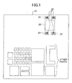
- FIG. 1 is a plan view of one embodiment of the printed wiring board device of the present invention.
- FIG. 2 is a diagram showing an example of the dummy part according to the present invention.
- FIG. 3 is a diagram showing another example of the dummy part according to the present invention.
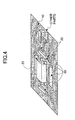
- FIG. 4 is a perspective view of one embodiment of the printed wiring board device of the present invention.
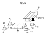
- FIG. 5 is a perspective view of another example of the dummy parts according to the present invention.
- FIG. 6 is a diagram for explaining a change of the surface temperature of a component part on a printed wiring board device in accordance with the elapsed time during reflow heating.
- FIG. 7 is a flowchart for explaining a method of manufacture of the printed wiring board device according to the present invention.
- FIG. 8 is a diagram for explaining each of respective steps of the manufacture method shown in FIG. 7.
- FIG. 9 is a plan view of a printed wiring board model that is used for a simulation test for comparison between the surface temperature of a target circuit part with the dummy parts and that of the target circuit part without the dummy parts.
- FIG. 10 is a diagram showing the surface temperature of the S-SOP and the physical properties of dummy parts in the vicinity of the S-SOP in each simulated result for a first example of the printed wiring board model.
- FIG. 11 is a plan view of the first example of the printed wiring board model for the simulation test.
- FIG. 12 is a diagram for explaining a change of the surface temperature of each of the circuit parts during the reflow heating which is obtained as simulation results of the first example of the printed wiring board model.
- FIG. 13 is a diagram showing the surface temperature of the S-SOP and the physical properties of dummy parts in the vicinity of the S-SOP in each simulated results of a second example of the printed wiring board model.
- FIG. 14 is a plan view of the second example of the printed wiring board model for the simulation test.
- FIG. 15 is a diagram for explaining a change of the surface temperature of each of the circuit parts during the reflow heating which is obtained as simulation results of the second example of the printed wiring board model.
- FIG. 16 is a diagram showing an information processing apparatus in which the printed wiring board device of the present invention is provided.
- FIG. 1 shows one embodiment of the printed wiring board device of the present invention.
- a circuit part 20 is mounted on the wiring board at a position isolated from other parts on the wiring board.
- the circuit part 20 constitutes a part of a circuit in the printed wiring board device 10.
- a plurality of pads 22 are provided on the wiring board in the vicinity of peripheral edges of the circuit part 20.
- the pads 22 are electrically isolated from the circuit in the printed wiring board device 10. Namely, there is no electrical connection between each pad 22 and the circuit.
- heat-absorbing dummy parts 30 are mounted on the pads 22, and the dummy parts 30 efficiently absorb heat from the circuit part 20 through the pads 22 during reflow soldering.
- the dummy parts are not circuit parts that constitute parts of a circuit in the printed wiring board device, but the dummy parts are provided on the wiring board adjacent to a circuit part in order to absorb or collect heat from the adjacent circuit part at the time of reflow soldering.
- FIG. 6 shows a change of the surface temperature of the circuit parts on the printed wiring board in accordance with the elapsed time during the reflow heating.
- the surface temperature of the circuit parts on the printed wiring board is gradually raised in accordance with the elapsed time (preliminary heating).
- the surface temperature is increased at a stretch so that all solder junctions on the wiring board are set to be higher than the melting point temperature (heating). In this state, the solder melting is attained so that the solder junctions between the individual parts on the wiring board are made.
- the temperature at which the surface temperature during the reflow heating is the maximum is called the peak temperature.
- the reflow soldering of the printed wiring board including the isolated parts is performed and the isolated parts have a low heat capacity, there is a problem in that the reflow heating temperature is rapidly raised and it may exceed the heat-resistant temperature of the isolated parts. Furthermore, when the leaded solder is changed to the unleaded solder, the melting point of the unleaded solder is raised from that of the leaded solder. In such a case, it is necessary to take measures for maintaining the isolated parts in a proper temperature range during the reflow heating, in order to prevent the peeling or swelling of the resin layer of the isolated parts.
- FIG. 4 shows another embodiment of the printed wiring board device of the present invention.
- the circuit part 20 has a low heat resistance and is mounted on the wiring board at a position isolated from other parts on the wiring board.
- the circuit part 20 constitutes a part of a circuit in the printed wiring board device 10.
- the circuit part 20 is an isolated circuit part that is subjected to excessive heating at the time of reflow soldering of the printed wiring board device 10.
- a superfluous temperature rise of the isolated circuit part 20 which exceeds a heat-resistant temperature thereof is likely to take place during the reflow soldering.
- the preventive measures for preventing the excessive heating of the isolated circuit part 20 during the reflow soldering are taken, as described below.
- the plurality of pads 22, which are electrically isolated from the circuit formed by the circuit part 20, are disposed on the wiring board in the vicinity of the peripheral edges of the circuit part 20.
- the heat-absorbing dummy parts 30 are mounted on the pads 22.
- a superfluous temperature rise of the circuit part 20 during the reflow heating can be prevented by increasing the heat capacity per unit area in the vicinity of the isolated circuit part 20 by means of the dummy parts 30.
- each dummy part 30 is mounted on the pads 22 which are not electrically connected with the circuit inside the printed wiring board device 10. Accordingly, even when the dummy parts 30 are added to the printed wiring board device 10, the influences of the dummy parts 20 on the internal circuit may be negligible.
- the dummy parts 30 are permanently mounted on the pads 22 of the printed wiring board device 10.
- the dummy parts 30 may be provided removably onto the printed wiring board device 10.
- the dummy parts 30 can suppress the change to the current printed wiring board design at a necessary, minimum level, and it is advantageous in respect of the manufacture cost.
- the dummy parts 30 are mounted in the circumference of one of the circuit parts (the circuit part 20 in FIG. 4) that receives during the reflow heating the largest amount of heat among the respective amounts of heat received by the circuit parts on the wiring board.
- the heat capacity is defined as being a quantity of heat needed for a 1-degree temperature rise of the part concerned, and it can be computed as a product of the specific heat (J/kg-K) of the part, the density (kg/m 3 ) of the part and the volume (m 3 ) of the part.
- the dummy parts 30 In order to prevent the excessive heating of the circuit part 20 during the reflow heating, it is necessary that the dummy parts 30 have a sufficiently large heat capacity in comparison with the heat-resistant temperature of the circuit part 20. It is preferred that the dummy parts 30 are configured so that they have a sufficiently large thermal conductivity as well as a sufficiently large heat capacity in comparison with the heat-resistant temperature of the circuit part 20.
- the dummy parts 30 having a large thermal conductivity promote the flow of heat from the external surfaces of the dummy parts 30 to the inside thereof, and the dummy parts 30 efficiently absorb the heat from the circuit part 20 during the reflow heating because they have a large heat capacity.
- the printed wiring board device 10 of the present embodiment it is possible for the printed wiring board device 10 of the present embodiment to prevent the temperature rise of the circuit part 20 during the reflow soldering from exceeding the heat-resistant temperature of the circuit part 30.
- the composition material of the dummy parts 30 that is suitable for the above purpose is one of ceramics (such as alumina), copper, an aluminum alloy, etc. If it is ensured that the dummy parts have a sufficiently large heat capacity, a metallic material, such as a stainless material, may be used as the suitable composition material of the dummy parts 30.
- a ceramic material is selected as being the composition material of the dummy parts 30, chip capacitors or chip resistors may be used as the dummy parts 30.
- a metallic material is selected as being the composition material of the dummy parts 30, it is desirable that the dummy parts 30 are fixed to the wiring board by using an adhesive agent or a mechanical junction.
- the plurality of pads 22 that are not electrically connected with the circuit inside the printed wiring board device 10 are mounted in the vicinity of the circuit parts 20.
- the present invention is not limited to this embodiment.
- the pads 22 on the printed wiring board device 10 it is possible to prevent the excessive heating of the circuit parts 20 during the reflow soldering.
- the dummy parts 30 are fixed to the wiring board in the vicinity of the circuit parts 20 without using the pads 22.
- the dummy parts 30 serve to absorb the heat from the circuit parts 20 through the adhesive agent during the reflow heating.
- the surfaces of the dummy parts 30 are colored substantially in black by painting or surface treatment.
- FIG. 2 shows an example of the dummy part according to the present invention.
- the dummy part 30 of this example is configured in a rectangular parallelepiped form.
- the form of the dummy parts 30 is not limited to this example.
- the dummy parts 30 according to the present invention may be configured in a pillar-like form or a variant-like form.
- Such examples of the dummy parts 30 have no significant differences with respect to the effect to prevent the excessive heating of the circuit parts 20 during the reflow soldering.
- FIG. 3 shows another example of the dummy part 30 according to the present invention.
- a heat-absorption part 32 for example, a metal part which has a sufficiently large thermal conductivity in comparison with the heat-resistant temperature of the circuit parts 20 is attached to the surface of each dummy part 30 by using an adhesive agent or a mechanical junction.
- FIG. 5 shows another example of the dummy part according to the present invention.
- a heat-absorption part 34 having a sufficiently large heat capacity and being configured to cover the two dummy parts 30 is additionally provided on the wiring board in the vicinity of the circuit part 20.
- the heat-absorption part 34 of the example, as shown in FIG. 5, has a groove formed on the bottom of the heat-absorption part 34, and the two adjacent dummy parts 30 are contained in the groove and fully covered with the heat-absorption part 34 when the heat-absorption part 34 is mounted on the wiring board.
- the heat-absorption part 34 of the present embodiment is arranged near the circuit part 20 on the side of the printed wiring board device that faces toward the conveyance direction in which the printed wiring board device is transferred to and passed through the reflow equipment. According to the present embodiment, the effect which prevents the excessive heating of the circuit part 20 during the reflow soldering can be increased even when the surface area of the circuit part 20 is relatively large.
- the heat-absorption part 34 may be configured to surround the entire circumference of the circuit part 20.
- FIG. 7 shows a method of manufacture of the printed wiring board device according to the present invention.
- FIG. 8 is a diagram for explaining each of respective steps of the manufacturing method in FIG. 7.
- the circuit parts 20 are mounted on the wiring board at positions isolated from other parts on the wiring board, and the circuit parts 20 constitute parts of a circuit in the printed wiring board device.
- the preventive measures for preventing the temperature rise of the circuit parts 20 during the reflow soldering from exceeding the heat-resistant temperature of the circuit parts 20 are taken as described below.
- the pads 22 are not electrically isolated from the circuit in the printed wiring board device 10 and are mounted on the wiring board in the vicinity of the circuit parts 20.
- the arrangement portions of the pads 22 in the printed wiring board device 10 are predetermined such that they are essentially the same as those of the previous embodiment.
- the solder paste 41 is applied to the pads 22 on the printed wiring board device 10 by using a known method, such as a screen printing method (S10).
- the circuit parts 40 which should be mounted on the printed wiring board device 10 are mounted on the wiring board (S20), as shown in FIG. 7 and FIG. 8 (B).
- the circuit parts 40 constitute parts of the circuit in the printed wiring board device 10.
- the dummy parts 30 are also mounted on the pads 22 of the printed wiring board device 10, similar to the circuit parts 40. Hence, the dummy parts 30 are mounted on the wiring board in the vicinity of the circuit parts 20.
- the printed wiring board device 10 is transferred to and passed through the reflow equipment, and the reflow soldering of the printed wiring board device 10 is performed by using the reflow equipment (S30).
- the reflow equipment As shown in FIG. 8 (C), the printed wiring board device 10 is heated by the heat convection and radiation within the reflow equipment, and the re-melting of the solder paste 41 is caused to produce solder junctions on the printed wiring board device 10.
- the dummy parts 30 absorb efficiently the heat from the circuit parts 20 through the pads 22 during the reflow soldering.
- the manufacturing method of the present embodiment is effective in maintaining the circuit parts 20 in proper temperature conditions during the reflow soldering, and it is ensured that good solder junctions of the circuit parts 20 are made on the wiring board.
- the appearance inspection of the printed wiring board device 10 is conducted, and the solder junctions of the individual parts thereof are inspected (S40), as shown in FIG. 7 and FIG. 8 (D).
- the dummy parts 30 are provided so that they have a sufficiently large heat capacity in comparison with the heat-resistant temperature of the circuit parts 20. It is preferred that the dummy parts 30 are configured so that they have a sufficiently large thermal conductivity as well as a sufficiently large heat capacity in comparison with the heat-resistant temperature of the circuit part 20. Moreover, in order to increase the effect which prevents the excessive heating of the circuit parts 20 during the reflow soldering, the plurality of such dummy parts 30 are arranged on the wiring board in the vicinity of the peripheral edges of the circuit parts 20. Furthermore, in order to more efficiently absorb the heat from the circuit parts 20 in the reflow heating step, it is desirable that the surfaces of the dummy parts 30 are colored substantially in black by painting or surface treatment.
- FIG. 9 shows a printed wiring board model 100 that is used for a simulation test for comparison between the surface temperature of the target circuit part with the dummy parts and that of the target circuit part without the dummy parts.
- the circuit parts which constitute parts of the circuit in the printed wiring board are provided as the non-isolated circuit parts.
- Such circuit parts include the 14-pin S-SOP (shrink small outline package) package 42, the three FET (field-effect transistor) transistors 43, the two coils 44, and the BGA (ball grid array) package 45.
- the 14-pin S-SOP package which is essentially the same as the package 42, is provided as the isolated circuit part 20 that is mounted at the position isolated from the circuit parts 42-45.
- the S-SOP package 20 also constitutes a part of the circuit in the printed wiring board. It is assumed that the isolated arrangement of the S-SOP package 20 is needed according to the restrictions of the part arrangement.
- the four dummy parts 30 are provided on the wiring board in the vicinity of the peripheral edges of the isolated circuit part 20 (the S-SOP package). Moreover, the size of the printed wiring board model 100 of FIG. 9 is about 120 mm x 120 mm.
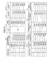
- FIG. 10 shows the surface temperature of the S-SOP and the physical properties of dummy parts in the vicinity of the S-SOP in each simulated result for a first example of the printed wiring board model.
- FIG. 11 is a plan view of the first example of the printed wiring board model for the simulation test.
- the Surface-A is the case where no dummy parts are provided in the vicinity of the isolated circuit part 20
- the Surface-B, the Surface-C, and the Surface-D are the cases where the dummy parts 30 which have different composition materials are provided, respectively, in the vicinity of the circuit part 20.
- the size of the coil 44 and the size of each of the respective dummy parts 30 of different composition materials are indicated.
- SOP indicates the small outline package is used as the material of the dummy parts 30.
- “CHIP” indicates the chip capacitor or resistor is used as the material of the dummy parts 30.
- SUS indicates the stainless material is used as the composition material of the dummy parts 30.
- GAP column of the table in FIG. 10 indicates that the gap between the coil 44 and the circuit part 42 or the gap between the dummy part 30 and the circuit part 20 is about 4 mm.
- the "TEMP. OF PART" column of the table in FIG. 10 indicates the surface temperature of the S-SOP part 42 or part 20 when the simulation test of the reflow heating is performed.
- the temperature of the non-isolated circuit part 42 is 220 deg. C
- the temperature of the circuit part 20 of the Surface-A wherein no dummy parts 30 are provided is 235 deg. C
- the respective temperatures of the circuit parts 20 of the Surface-B, the Surface-C and the Surface-D wherein the dummy parts 30 of the present invention are provided are decreased to 223 deg. C - 230 deg. C.
- the dummy parts 30 of the present invention serve to efficiently absorb the heat from the circuit part 20 during the reflow heating.
- FIG. 12 shows a change of the surface temperature of each of the isolated circuit parts during the reflow heating which is obtained as simulation results of the first example of the printed wiring board model 100-1.
- "42Q" indicates the point of measurement of the surface temperature of the non-isolated circuit part 42
- "20A” through “20D” respectively indicate the points of measurement of the surface temperatures of the isolated circuit parts 20 of the Surface-A through the Surface-D in the printed wiring board model 100-1.
- FIG. 13 shows the surface temperature of the S-SOP and the physical properties of dummy parts in the vicinity of the S-SOP in each simulated results of a second example of the printed wiring board model.
- FIG. 14 is a plan view of the second example of the printed wiring board model for the simulation test.
- composition material of the dummy parts 30 and the number thereof are changed, and the second example is provided to consider the change of the preventive effects that prevent the excessive heating of the isolated circuit part 20 during the reflow heating.
- the heat capacity of the dummy parts 30 of the Surface-A through the Surface-H and the thermal conductivity thereof are varied, and the change of the preventive effects according to the dummy parts 30 is taken into consideration.
- the "TEMP. OF PART" column of the table in FIG. 13 indicates the surface temperature of the S-SOP circuit parts 20 when the simulation test of the reflow heating is performed.
- the temperature of the circuit part 20 of the Surface-A wherein no dummy parts are provided is 235 deg. C
- the respective temperatures of the circuit parts 20 of the Surface-B through the Surface-H wherein the dummy parts 30 of the present invention are decreased to 223 deg. C - 230 deg. C.
- the dummy parts 30 of the present invention serve to efficiently absorb the heat from the circuit part 20 during the reflow heating.
- the preventive effects of the dummy parts 30 having a large thermal conductivity are higher than the preventive effects of the dummy parts 30 having a small thermal conductivity.
- the composition material of the dummy parts 30 having a large specific heat value in order to ensure that the heat capacity of the dummy parts 30 is sufficiently large.
- the volume of the dummy parts 30 is restricted, it is possible to compensate for the restriction of the volume by choosing the composition material of the dummy parts 30 having a large density value.
- the heat capacity of each dummy part 30 can be computed as a product of the specific heat (J/kg-K) of the dummy part, the density (kg/m 3 ) of the dummy part and the volume (m 3 ) of the dummy part.
- FIG. 15 shows a change of the surface temperature of each of the circuit parts during the reflow heating which is obtained as simulation results of the second example of the printed wiring board model.
- "20A” through “20H” respectively indicate the points of measurement of the surface temperatures of the circuit parts 20 of the Surface-A through the Surface-H in the printed wiring board model 100-2.
- FIG. 16 shows an example of an information processing apparatus in which the printed wiring board device according to the present invention is provided.
- the example in FIG. 16 is a main component 50 of a personal computer in which the printed wiring board device 10 according to the previous embodiment of FIG. 1 or FIG. 4 is provided.
- the personal computer is provided as the information processing apparatus.
- the circuit parts provided on the printed wiring board device 10 constitutes parts of an information processing circuit (for example, a data reading circuit) which processes information.
- the isolated circuit parts 20 are arranged at positions isolated from other parts on the wiring board and constitute parts of the information processing circuit.
- the pads are provided on the wiring board in the circumference of the circuit parts and electrically isolated from the circuit, and the dummy parts are mounted on the pads and absorb heat from the circuit parts through the pads during the reflow soldering. Even if the circuit parts having a low thermal resistance are needed to be isolated from other parts on the wiring board, it is possible to prevent the temperature rise of the circuit parts during the reflow soldering from exceeding the heat-resistant temperature thereof.
- the printed wiring board device 10 in the present embodiment of the information processing apparatus is effective in maintaining the circuit parts in proper temperature conditions, and it can ensure that good solder junctions are made on the wiring board, similar to the previous embodiment of FIG. 1 or FIG. 4. It is possible for the present embodiment to provide an information processing apparatus that is equipped with the printed wiring board device in which good solder junctions are made on the wiring board without causing defects.
Landscapes
- Engineering & Computer Science (AREA)
- Microelectronics & Electronic Packaging (AREA)
- Manufacturing & Machinery (AREA)
- Electric Connection Of Electric Components To Printed Circuits (AREA)
- Structure Of Printed Boards (AREA)
Applications Claiming Priority (2)
| Application Number | Priority Date | Filing Date | Title |
|---|---|---|---|
| JP2001381326A JP3816380B2 (ja) | 2001-12-14 | 2001-12-14 | 吸熱用ダミー部品を備えた基板ユニット及びその製造方法 |
| JP2001381326 | 2001-12-14 |
Publications (3)
| Publication Number | Publication Date |
|---|---|
| EP1320288A2 true EP1320288A2 (fr) | 2003-06-18 |
| EP1320288A3 EP1320288A3 (fr) | 2004-10-13 |
| EP1320288B1 EP1320288B1 (fr) | 2009-04-15 |
Family
ID=19187321
Family Applications (1)
| Application Number | Title | Priority Date | Filing Date |
|---|---|---|---|
| EP02255035A Expired - Lifetime EP1320288B1 (fr) | 2001-12-14 | 2002-07-17 | Dispositif de panneau à circuit imprimé et son procédé de fabrication |
Country Status (4)
| Country | Link |
|---|---|
| US (1) | US6787711B2 (fr) |
| EP (1) | EP1320288B1 (fr) |
| JP (1) | JP3816380B2 (fr) |
| DE (1) | DE60231952D1 (fr) |
Cited By (3)
| Publication number | Priority date | Publication date | Assignee | Title |
|---|---|---|---|---|
| EP2019574A3 (fr) * | 2007-07-25 | 2009-07-08 | TDK Corporation | Carte intégrée dans un composant électronique et son procédé de fabrication |
| EP2276329A1 (fr) * | 2009-07-16 | 2011-01-19 | ABB Research Ltd. | Carte de circuit électronique dotée d'un condensateur thermique |
| US8237059B2 (en) | 2007-07-25 | 2012-08-07 | Tdk Corporation | Electronic component-embedded board and method of manufacturing the same |
Families Citing this family (3)
| Publication number | Priority date | Publication date | Assignee | Title |
|---|---|---|---|---|
| US10879211B2 (en) | 2016-06-30 | 2020-12-29 | R.S.M. Electron Power, Inc. | Method of joining a surface-mount component to a substrate with solder that has been temporarily secured |
| JP6737221B2 (ja) | 2017-04-11 | 2020-08-05 | 株式会社デンソー | 電動パワーステアリング制御装置および電子ユニット。 |
| JP7543863B2 (ja) * | 2020-11-17 | 2024-09-03 | 富士電機株式会社 | 半導体モジュール |
Family Cites Families (16)
| Publication number | Priority date | Publication date | Assignee | Title |
|---|---|---|---|---|
| JPH02113512A (ja) * | 1988-10-21 | 1990-04-25 | Matsushita Electric Ind Co Ltd | フィルムコンデンサ |
| US4941067A (en) * | 1989-04-07 | 1990-07-10 | Motorola Inc. | Thermal shunt for electronic circuits |
| JPH02309602A (ja) * | 1989-05-24 | 1990-12-25 | Matsushita Electric Ind Co Ltd | 角形チップ抵抗器 |
| US5128506A (en) * | 1990-10-30 | 1992-07-07 | Westinghouse Electric Corp. | Method and apparatus for selective infrared soldering using shielding fixtures |
| US6021046A (en) * | 1993-06-09 | 2000-02-01 | Dallas Semiconductor Corporation | Thermal protection of electrical elements systems |
| JPH0737337A (ja) | 1993-07-08 | 1995-02-07 | Hitachi Ltd | ディジタル信号記録再生方法およびその装置 |
| JPH0888463A (ja) * | 1994-09-19 | 1996-04-02 | Fujitsu Ltd | 電子部品のはんだ付け実装方法 |
| JPH08213724A (ja) * | 1995-01-31 | 1996-08-20 | Mitsumi Electric Co Ltd | 回路基板 |
| JPH1022335A (ja) * | 1996-06-28 | 1998-01-23 | Toyota Motor Corp | ハンダ膜厚制御方法 |
| DE69812570T2 (de) * | 1997-12-24 | 2004-01-29 | Denso Corp | Gerät mit Leiterplatte und dessen Zusammenbauverfahren |
| US6281573B1 (en) * | 1998-03-31 | 2001-08-28 | International Business Machines Corporation | Thermal enhancement approach using solder compositions in the liquid state |
| US6034875A (en) * | 1998-06-17 | 2000-03-07 | International Business Machines Corporation | Cooling structure for electronic components |
| US6175500B1 (en) * | 1998-09-22 | 2001-01-16 | Lucent Technologies Inc. | Surface mount thermal connections |
| JP2000114674A (ja) * | 1998-10-08 | 2000-04-21 | Sony Corp | 伝熱部を備えるプリント回路板およびプリント配線基板 |
| JP2001085827A (ja) | 1999-09-14 | 2001-03-30 | Fuji Xerox Co Ltd | プリント配線基板 |
| JP2001291741A (ja) * | 2000-04-06 | 2001-10-19 | Nec Corp | 半導体集積回路実装方法及び半導体集積回路装置 |
-
2001
- 2001-12-14 JP JP2001381326A patent/JP3816380B2/ja not_active Expired - Fee Related
-
2002
- 2002-07-16 US US10/195,547 patent/US6787711B2/en not_active Expired - Lifetime
- 2002-07-17 EP EP02255035A patent/EP1320288B1/fr not_active Expired - Lifetime
- 2002-07-17 DE DE60231952T patent/DE60231952D1/de not_active Expired - Lifetime
Cited By (3)
| Publication number | Priority date | Publication date | Assignee | Title |
|---|---|---|---|---|
| EP2019574A3 (fr) * | 2007-07-25 | 2009-07-08 | TDK Corporation | Carte intégrée dans un composant électronique et son procédé de fabrication |
| US8237059B2 (en) | 2007-07-25 | 2012-08-07 | Tdk Corporation | Electronic component-embedded board and method of manufacturing the same |
| EP2276329A1 (fr) * | 2009-07-16 | 2011-01-19 | ABB Research Ltd. | Carte de circuit électronique dotée d'un condensateur thermique |
Also Published As
| Publication number | Publication date |
|---|---|
| JP3816380B2 (ja) | 2006-08-30 |
| US20030111262A1 (en) | 2003-06-19 |
| DE60231952D1 (de) | 2009-05-28 |
| EP1320288A3 (fr) | 2004-10-13 |
| JP2003188506A (ja) | 2003-07-04 |
| EP1320288B1 (fr) | 2009-04-15 |
| US6787711B2 (en) | 2004-09-07 |
Similar Documents
| Publication | Publication Date | Title |
|---|---|---|
| TW563230B (en) | Semiconductor device having a ball grid array and method therefor | |
| US5172852A (en) | Soldering method | |
| CA2273752A1 (fr) | Zones de collecte de boules de soudure anti-pontage | |
| Marcoux | Fine pitch surface mount technology: quality, design, and manufacturing techniques | |
| US20090050677A1 (en) | Method of welding electronic components on pcbs | |
| US20120325540A1 (en) | Footprint on pcb for leadframe-based packages | |
| EP1320288B1 (fr) | Dispositif de panneau à circuit imprimé et son procédé de fabrication | |
| US20130048360A1 (en) | System in package, printed circuit board provided with such system in package | |
| US7443685B2 (en) | Conductive heat transfer for electrical devices from the solder side and component side of a circuit card assembly | |
| JP2010177274A (ja) | 電子部品実装基板及び電子部品実装基板の製造方法 | |
| CN1874654B (zh) | 焊接方法、电子部件和部件调换方法 | |
| US20080023840A1 (en) | Via heat sink material | |
| JP2003249746A (ja) | プリント基板 | |
| JP4016389B2 (ja) | プリント配線基板の検査装置及び検査方法 | |
| US20060006533A1 (en) | Motherboard structure for preventing short circuit | |
| KR200317709Y1 (ko) | 전자부품용 방열판 및 그 장착구조 | |
| JPH10294399A (ja) | Bgaパッケージの実装構造 | |
| JPS60100495A (ja) | 電子部品の実装方法 | |
| Cognetti et al. | Resistance to soldering heat and thermal characteristics of plastic SMDs | |
| JP2553989Y2 (ja) | 電子部品 | |
| Schiebel | Automatic gang bonding, the alternative process | |
| JPH02244648A (ja) | 電子部品の実装方法およびそれに用いる表面実装形電子部品と実装基板 | |
| JPS60208893A (ja) | 混成厚膜集積回路の製造方法 | |
| JPS61141198A (ja) | 回路部品の混載実装方法 | |
| Kern et al. | BGA Reliability of Large Organic Flip-Chip Carriers |
Legal Events
| Date | Code | Title | Description |
|---|---|---|---|
| PUAI | Public reference made under article 153(3) epc to a published international application that has entered the european phase |
Free format text: ORIGINAL CODE: 0009012 |
|
| AK | Designated contracting states |
Designated state(s): AT BE BG CH CY CZ DE DK EE ES FI FR GB GR IE IT LI LU MC NL PT SE SK TR |
|
| AX | Request for extension of the european patent |
Extension state: AL LT LV MK RO SI |
|
| PUAL | Search report despatched |
Free format text: ORIGINAL CODE: 0009013 |
|
| AK | Designated contracting states |
Kind code of ref document: A3 Designated state(s): AT BE BG CH CY CZ DE DK EE ES FI FR GB GR IE IT LI LU MC NL PT SE SK TR |
|
| AX | Request for extension of the european patent |
Extension state: AL LT LV MK RO SI |
|
| 17P | Request for examination filed |
Effective date: 20041108 |
|
| AKX | Designation fees paid |
Designated state(s): DE FR GB |
|
| GRAP | Despatch of communication of intention to grant a patent |
Free format text: ORIGINAL CODE: EPIDOSNIGR1 |
|
| GRAS | Grant fee paid |
Free format text: ORIGINAL CODE: EPIDOSNIGR3 |
|
| GRAA | (expected) grant |
Free format text: ORIGINAL CODE: 0009210 |
|
| AK | Designated contracting states |
Kind code of ref document: B1 Designated state(s): DE FR GB |
|
| REG | Reference to a national code |
Ref country code: GB Ref legal event code: FG4D |
|
| REF | Corresponds to: |
Ref document number: 60231952 Country of ref document: DE Date of ref document: 20090528 Kind code of ref document: P |
|
| PLBE | No opposition filed within time limit |
Free format text: ORIGINAL CODE: 0009261 |
|
| STAA | Information on the status of an ep patent application or granted ep patent |
Free format text: STATUS: NO OPPOSITION FILED WITHIN TIME LIMIT |
|
| 26N | No opposition filed |
Effective date: 20100118 |
|
| REG | Reference to a national code |
Ref country code: FR Ref legal event code: PLFP Year of fee payment: 15 |
|
| REG | Reference to a national code |
Ref country code: FR Ref legal event code: PLFP Year of fee payment: 16 |
|
| PGFP | Annual fee paid to national office [announced via postgrant information from national office to epo] |
Ref country code: FR Payment date: 20170613 Year of fee payment: 16 |
|
| PGFP | Annual fee paid to national office [announced via postgrant information from national office to epo] |
Ref country code: DE Payment date: 20170711 Year of fee payment: 16 Ref country code: GB Payment date: 20170712 Year of fee payment: 16 |
|
| REG | Reference to a national code |
Ref country code: DE Ref legal event code: R119 Ref document number: 60231952 Country of ref document: DE |
|
| GBPC | Gb: european patent ceased through non-payment of renewal fee |
Effective date: 20180717 |
|
| PG25 | Lapsed in a contracting state [announced via postgrant information from national office to epo] |
Ref country code: GB Free format text: LAPSE BECAUSE OF NON-PAYMENT OF DUE FEES Effective date: 20180717 Ref country code: FR Free format text: LAPSE BECAUSE OF NON-PAYMENT OF DUE FEES Effective date: 20180731 Ref country code: DE Free format text: LAPSE BECAUSE OF NON-PAYMENT OF DUE FEES Effective date: 20190201 |