EP1324308A1 - Système de génération des tensions de commutation lignes et colonnes pour afficheurs à cristaux liquides - Google Patents
Système de génération des tensions de commutation lignes et colonnes pour afficheurs à cristaux liquides Download PDFInfo
- Publication number
- EP1324308A1 EP1324308A1 EP01830809A EP01830809A EP1324308A1 EP 1324308 A1 EP1324308 A1 EP 1324308A1 EP 01830809 A EP01830809 A EP 01830809A EP 01830809 A EP01830809 A EP 01830809A EP 1324308 A1 EP1324308 A1 EP 1324308A1
- Authority
- EP
- European Patent Office
- Prior art keywords
- voltage
- rows
- voltages
- intermediary
- liquid crystal
- Prior art date
- Legal status (The legal status is an assumption and is not a legal conclusion. Google has not performed a legal analysis and makes no representation as to the accuracy of the status listed.)
- Withdrawn
Links
- 239000004973 liquid crystal related substance Substances 0.000 title claims abstract description 27
- 230000001105 regulatory effect Effects 0.000 description 9
- 230000007704 transition Effects 0.000 description 5
- XUIMIQQOPSSXEZ-UHFFFAOYSA-N Silicon Chemical compound [Si] XUIMIQQOPSSXEZ-UHFFFAOYSA-N 0.000 description 2
- 229910052710 silicon Inorganic materials 0.000 description 2
- 239000010703 silicon Substances 0.000 description 2
- 230000001174 ascending effect Effects 0.000 description 1
- 238000000034 method Methods 0.000 description 1
Images



Classifications
-
- G—PHYSICS
- G09—EDUCATION; CRYPTOGRAPHY; DISPLAY; ADVERTISING; SEALS
- G09G—ARRANGEMENTS OR CIRCUITS FOR CONTROL OF INDICATING DEVICES USING STATIC MEANS TO PRESENT VARIABLE INFORMATION
- G09G3/00—Control arrangements or circuits, of interest only in connection with visual indicators other than cathode-ray tubes
- G09G3/20—Control arrangements or circuits, of interest only in connection with visual indicators other than cathode-ray tubes for presentation of an assembly of a number of characters, e.g. a page, by composing the assembly by combination of individual elements arranged in a matrix no fixed position being assigned to or needed to be assigned to the individual characters or partial characters
- G09G3/34—Control arrangements or circuits, of interest only in connection with visual indicators other than cathode-ray tubes for presentation of an assembly of a number of characters, e.g. a page, by composing the assembly by combination of individual elements arranged in a matrix no fixed position being assigned to or needed to be assigned to the individual characters or partial characters by control of light from an independent source
- G09G3/36—Control arrangements or circuits, of interest only in connection with visual indicators other than cathode-ray tubes for presentation of an assembly of a number of characters, e.g. a page, by composing the assembly by combination of individual elements arranged in a matrix no fixed position being assigned to or needed to be assigned to the individual characters or partial characters by control of light from an independent source using liquid crystals
- G09G3/3611—Control of matrices with row and column drivers
- G09G3/3696—Generation of voltages supplied to electrode drivers
-
- G—PHYSICS
- G09—EDUCATION; CRYPTOGRAPHY; DISPLAY; ADVERTISING; SEALS
- G09G—ARRANGEMENTS OR CIRCUITS FOR CONTROL OF INDICATING DEVICES USING STATIC MEANS TO PRESENT VARIABLE INFORMATION
- G09G2330/00—Aspects of power supply; Aspects of display protection and defect management
- G09G2330/02—Details of power systems and of start or stop of display operation
- G09G2330/021—Power management, e.g. power saving
Definitions
- the present invention refers to a generation system for driving voltages of the rows and of the columns of a liquid crystal display.
- the first voltage level is called Vlcd and it is directly proportional to the lighting threshold of the liquid crystal and to the square root of the number of the driven rows.
- the other four voltage levels V2, V3, V4 and V5 are distributed between the Vlcd and GND voltages according to a law that depends on the square root of the number of the driven rows.
- the different voltage levels are applied to the rows and columns with alternate phase in order to cancel the direct component of the voltage applied to the display, harmful for the liquid crystal. More particularly, in a frame period, or part of it, the rows are driven between the voltages V5 and Vlcd, while in the following period the rows are driven between the voltages GND and V2, in the same way the columns are driven between the voltages GND and V4 and between the voltages V3 and Vlcd.
- the voltage Vlcd is generated by a charging pump starting from the supply voltage Vdd, while the other four voltage levels V2, V3, V4 and V5 are obtained from intermediary dividers of Vlcd, and applied to voltage followers that work as buffer circuits, normally supplied between the voltages Vlcd and GND.
- the Applicant noticed that in this case the charge quantity, determined during a transition from the voltage Vlcd to the voltage V3 and equal to Cx(Vlcd - V3), where Cx is the capacity of the pixel, is transferred to ground GND. Similarly he noticed that the charge quantity determined during a transition from the voltage GND to the voltage V4, equal to Cx* V4, is taken from the supply voltage Vlcd.
- an object of the present invention is to provide a generation system for driving voltages of the rows and of the columns of a liquid crystal display with greater efficiency than the known art.
- a generation system for driving voltages of the rows and of the columns of a liquid crystal display comprising: a first supply voltage; a second supply voltage; said first and second supply voltage supply a voltage generator circuit that provides at its output a first, a second, a third and a fourth voltage having respectively four prefixed values; characterized by further comprising at least one voltage generator that provides a first intermediary voltage having a first intermediary prefixed value of intermediary value with respect to said first and second supply voltages, said first intermediary voltage supplies part of said voltage generator circuit.
- the present invention it is possible to realize a generation system for driving voltages of the rows and of the columns of a liquid crystal display having a reduced power consumption.
- the supply voltage Vdd supplies a positive charging pump 1 or, otherwise said, voltage converter, that provides in output the voltage Vddbis.
- the voltage Vddbis supplies an operational amplifier OP1 that provides a voltage Vlcd in output.
- the voltage Vlcd is applied to a terminal of a variable resistance P1, the other terminal of P1 is connected to ground GND.
- the cursor of the variable resistance P1 is connected to the negative terminal of the operational amplifier OP1.
- a reference voltage Vref produced by a voltage generator 2 is connected to the positive terminal of the operational amplifier OP1.
- the voltage Vlcd is applied to a resistance divider R1-R5 in turn connected to ground GND.
- the positive inputs of the operational amplifiers denominated respectively OP2-OP5 are applied in the junction nodes between a resistance and an other.
- the negative terminals of the operational amplifiers OP2-OP5 are connected to the respective outputs of the operational amplifiers OP2-OP5, as to constitute voltage followers.
- the operational amplifiers OP2-OP5 produce respectively the voltages V2-V5 at their output.
- the operational amplifiers OP2-OP5, in the embodiment of figure 1, are supplied between the voltages Vlcd and GND.
- the voltage generator 2 is designed so that it compensates the thermal variations and eventually other factors of the liquid crystal display.
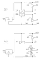
- figure 2 represents schematically a first embodiment of a generation system for driving voltages of the rows and of the columns of a liquid crystal display according to the present invention.
- a positive charging pump 21 supplied by the voltage Vdd and referred to ground produces the voltage Vlcd in output. It is assumed for simplicity that the charging pump 21 also comprises the circuit of figure 1 constituted by the variable resistance P1, by the operational amplifier OP1 and by the voltage generator 2. Besides, also like below, the resistance divider R1-R5 is not represented for simplicity.
- a negative charging pump 22 supplied by the voltage Vdd and referred to the voltage Vlcd produces the voltage V3bis in output.
- the operational amplifiers OP2 and OP3, here represented schematically for illustrative simplicity, are supplied between the voltages Vlcd and V3bis.
- a positive charging pump 23 supplied by the voltage Vdd and referred to the voltage GND produces the voltage V4bis in output.
- the operational amplifiers OP4 and OP5, also here represented schematically for illustrative simplicity, are supplied between the voltages V4bis and GND.
- the charging pumps are referred to the voltages as above described but they can also be referred to other voltages in the system, for example the negative charging pumps 22, 32, 42, 52 can be referred to Vddbis, and the positive charging pumps 21, 31, 41, 51, 23, 43 can be referred to Vdd.
- the voltage Vlcd As upper voltage it is reported the voltage Vlcd, but also another voltage as for instance the voltage Vddbis (of figure 1) can be used, by adding a similar circuit to that of figure 1 for the generation of the voltage Vlcd.
- Vdd 1,6V
- V2 8V
- V3 7V
- V4 2V
- V5 1V
- the advantage will be therefore that the quantity of charge determined during a transition between a voltage and an other will be of considerably lower entity than in the known art, with a consequent small current consumption.
- figure 3 represents schematically a second embodiment of a generation system for driving voltages of the rows and of the columns of a liquid crystal display according to the present invention.
- a positive charging pump 31 supplied by the voltage Vdd and referred to ground produces the voltage Vlcd in output.
- the charging pump 31 also comprises the circuit of figure 1 constituted by the variable resistance P1, by the operational amplifier OP1 and by the voltage generator 2.
- a negative charging pump 32 supplied by the voltage Vdd and referred to the voltage Vlcd produces the voltage V3bis in output.
- the operational amplifiers OP2 and OP3, here represented schematically for illustrative simplicity, are supplied between the voltages Vlcd and V3bis.
- the operational amplifiers OP4 and OP5 also here represented schematically for illustrative simplicity, are supplied between the voltage Vdd and GND, if the voltage Vdd is greater than V4, but they can also be supplied with the voltage Vlcd or V3bis.
- the positive charging pump 23 is eliminated.
- figure 4 represents schematically a third embodiment of a generation system for driving voltages of the rows and of the columns of a liquid crystal display according to the present invention.
- a positive charging pump 41 supplied by the voltage Vdd and referred to ground produces the voltage Vlcd in output.
- the charging pump 41 also comprises the circuit of figure 1 constituted by the variable resistance P1, by the operational amplifier OP1 and by the voltage generator 2.
- a negative regulated charging pump 42 supplied by the voltage Vdd and referred to the voltage Vlcd produces the voltage V3 in output.
- the operational amplifier OP2 here represented schematically for illustrative simplicity, is supplied between the voltage Vlcd and V3.
- a positive regulated charging pump 43 supplied by the voltage Vdd and referred to the GND voltage produces the voltage V4 in output.
- the operational amplifier OP4 also here represented schematically for illustrative simplicity, is supplied between the voltages V4 and GND.
- the charging pumps 42 and 43 are defined regulated in the sense that they must supply directly the voltages V3 and V4 in output, and they therefore present a feedback loop for the output voltage control, as can be seen from figure 6 subsequently.
- figure 5 represents schematically a fourth embodiment of a generation system for driving voltages of the rows and of the columns of a liquid crystal display according to the present invention.
- a positive charging pump 51 supplied by the voltage Vdd and referred to ground produces in output the voltage Vlcd.
- the charging pump 51 also comprises the circuit of figure 1 constituted by the variable resistance P1, by the operational amplifier OP1 and by the voltage generator 2.
- a negative regulated charging pump 52 supplied by the voltage Vdd and referred to the voltage Vlcd produces the voltage V3 in output.
- the operational amplifier OP2 here represented schematically for illustrative simplicity, is supplied between the voltage Vlcd and V3.
- the charging pump 52 is defined regulated in the sense that it must supply the voltage V3 directly in output.
- the positive charging pump 43 is eliminated.
- circuits 22, 23, 32, 42, 43 and 52 are defined as charging pumps but they can be substituted by any other kind of voltage converter able to provide the voltage levels above defined in output.
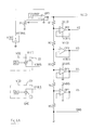
- figure 6A represents schematically an implementation of the scheme of figure 2, according the present invention.
- FIG 6A the scheme of figure 1 has been modified by inserting the implementation of the negative charging pump 22 and of the positive charging pump 23, composed respectively by an oscillator 24 and 26 and by a controlled generator 25 and 27, that produce the voltage V3bis and the voltage V4bis respectively.
- the voltages V3bis and V4bis supply the operational amplifiers OP2-OP5.
- Such a circuit can be simplified unifying the oscillator signal of the charging pumps 22 and 23, generating it with only one common oscillator.
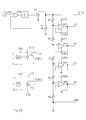
- figure 7 schematically represents an implementation of the scheme of figure 4.
- FIG 7A the scheme of figure 1 has been modified by inserting the implementation of the negative regulated charging pump 42 and of the positive regulated charging pump 43, schematised respectively by an operational amplifier OP6 and OP7 whose output is connected to a voltage controlled oscillator 44 and 45 and by a controlled generator 46 and 47, that produce the voltage V3 and the voltage V4 respectively in output.
- the negative input of the operational amplifier OP6 is connected to the connection point between the resistance R2 and the resistance R3.
- the positive input of the operational amplifier OP6 is connected to the voltage V3.
- the positive input of the operational amplifier OP7 is connected to the connection point between the resistance R3 to the resistance R4.
- the negative input of the operational amplifier OP7 is connected to the voltage V4.
- the voltages V3 and V4 supply the operational amplifiers OP2 and OP5 as above described.
- the charging pumps 21, 31, 41 and 51 are defined as comprising the circuits of figure 1 that starting from the supply voltage Vdd provides the voltage Vlcd in output, but they can be also constituted by regulated positive charging pumps as for example the regulated positive charging pump 43.
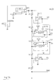
- the scheme of figure 6A has been modified implementing the charging pump that provides the voltage Vlcd, by means of a voltage generator 2 that produces a reference voltage Vref, that is applied to the positive input of an operational amplifier OP8.
- the output of the operational amplifier OP8 is connected to a voltage controlled oscillator 61 that controls a controlled generator 62, which produces the voltage Vlcd in output.
- the voltage Vlcd is applied to a terminal of a variable resistance P1, the other terminal of P1 is connected to ground GND.
- the cursor of the variable resistance P1 is connected to the negative terminal of the operational amplifier OP8.
- FIG 7B the scheme of figure 7A has been modified implementing the charging pump that provides the voltage Vlcd, by means of a voltage generator 2 that produces a reference voltage Vref, that is applied to the positive input of an operational amplifier OP9.
- the output of the operational amplifier OP9 is connected to a voltage controlled oscillator 71 that control a controlled generator 72, which produces the voltage Vlcd in output.
- the voltage Vlcd is applied to a terminal of a variable resistance P1, the other terminal of P1 is connected to ground GND.
- the cursor of the variable resistance P1 is connected to the negative terminal of the operational amplifier OP9.
Landscapes
- Engineering & Computer Science (AREA)
- Chemical & Material Sciences (AREA)
- Crystallography & Structural Chemistry (AREA)
- Physics & Mathematics (AREA)
- Computer Hardware Design (AREA)
- General Physics & Mathematics (AREA)
- Theoretical Computer Science (AREA)
- Liquid Crystal Display Device Control (AREA)
- Liquid Crystal (AREA)
Priority Applications (2)
| Application Number | Priority Date | Filing Date | Title |
|---|---|---|---|
| EP01830809A EP1324308A1 (fr) | 2001-12-27 | 2001-12-27 | Système de génération des tensions de commutation lignes et colonnes pour afficheurs à cristaux liquides |
| US10/326,724 US20030122766A1 (en) | 2001-12-27 | 2002-12-20 | Generation system for driving voltages of the rows and of the columns of a liquid crystal display |
Applications Claiming Priority (1)
| Application Number | Priority Date | Filing Date | Title |
|---|---|---|---|
| EP01830809A EP1324308A1 (fr) | 2001-12-27 | 2001-12-27 | Système de génération des tensions de commutation lignes et colonnes pour afficheurs à cristaux liquides |
Publications (1)
| Publication Number | Publication Date |
|---|---|
| EP1324308A1 true EP1324308A1 (fr) | 2003-07-02 |
Family
ID=8184839
Family Applications (1)
| Application Number | Title | Priority Date | Filing Date |
|---|---|---|---|
| EP01830809A Withdrawn EP1324308A1 (fr) | 2001-12-27 | 2001-12-27 | Système de génération des tensions de commutation lignes et colonnes pour afficheurs à cristaux liquides |
Country Status (2)
| Country | Link |
|---|---|
| US (1) | US20030122766A1 (fr) |
| EP (1) | EP1324308A1 (fr) |
Families Citing this family (4)
| Publication number | Priority date | Publication date | Assignee | Title |
|---|---|---|---|---|
| CN101000738A (zh) * | 2006-01-11 | 2007-07-18 | 松下电器产业株式会社 | 电压产生系统 |
| JP5189147B2 (ja) * | 2010-09-02 | 2013-04-24 | 奇美電子股▲ふん▼有限公司 | ディスプレイ装置及びこれを有する電子機器 |
| US9898992B2 (en) | 2011-07-01 | 2018-02-20 | Sitronix Technology Corp. | Area-saving driving circuit for display panel |
| US11069318B2 (en) * | 2011-07-01 | 2021-07-20 | Sitronix Technology Corp. | Driving circuit for display panel |
Citations (6)
| Publication number | Priority date | Publication date | Assignee | Title |
|---|---|---|---|---|
| JPS6368819A (ja) * | 1986-09-10 | 1988-03-28 | Casio Comput Co Ltd | 液晶駆動電圧発生回路 |
| EP0772067A1 (fr) * | 1995-05-17 | 1997-05-07 | Seiko Epson Corporation | Affichage a cristaux liquides, son procede d'excitation, circuit d'excitation et alimentation electrique employes a cet effet |
| US6232944B1 (en) * | 1996-04-05 | 2001-05-15 | Matsushita Electric Industrial Co., Ltd. | Driving method, drive IC and drive circuit for liquid crystal display |
| US20010013864A1 (en) * | 1997-07-09 | 2001-08-16 | Ryohei Kakuta | Driving voltage generator of liquid crystal display unit |
| US6281890B1 (en) * | 1997-06-19 | 2001-08-28 | Kabushiki Kaisha Toshiba | Liquid crystal drive circuit and liquid crystal display system |
| US6317122B1 (en) * | 1995-01-11 | 2001-11-13 | Seiko Epson Corporation | Power circuit, liquid crystal display device, and electronic equipment |
Family Cites Families (6)
| Publication number | Priority date | Publication date | Assignee | Title |
|---|---|---|---|---|
| JP2695981B2 (ja) * | 1990-10-05 | 1998-01-14 | 株式会社東芝 | 液晶表示器駆動電源回路 |
| JPH06180564A (ja) * | 1992-05-14 | 1994-06-28 | Toshiba Corp | 液晶表示装置 |
| JP3234043B2 (ja) * | 1993-05-10 | 2001-12-04 | 株式会社東芝 | 液晶駆動用電源回路 |
| CN1129887C (zh) * | 1994-12-26 | 2003-12-03 | 夏普公司 | 液晶显示装置 |
| JP3477714B2 (ja) * | 1995-01-13 | 2003-12-10 | セイコーエプソン株式会社 | 電源回路、液晶表示体駆動用電源及び液晶表示装置 |
| JP3132470B2 (ja) * | 1998-06-08 | 2001-02-05 | 日本電気株式会社 | 液晶表示パネル駆動用電源回路とその消費電力低減方法 |
-
2001
- 2001-12-27 EP EP01830809A patent/EP1324308A1/fr not_active Withdrawn
-
2002
- 2002-12-20 US US10/326,724 patent/US20030122766A1/en not_active Abandoned
Patent Citations (6)
| Publication number | Priority date | Publication date | Assignee | Title |
|---|---|---|---|---|
| JPS6368819A (ja) * | 1986-09-10 | 1988-03-28 | Casio Comput Co Ltd | 液晶駆動電圧発生回路 |
| US6317122B1 (en) * | 1995-01-11 | 2001-11-13 | Seiko Epson Corporation | Power circuit, liquid crystal display device, and electronic equipment |
| EP0772067A1 (fr) * | 1995-05-17 | 1997-05-07 | Seiko Epson Corporation | Affichage a cristaux liquides, son procede d'excitation, circuit d'excitation et alimentation electrique employes a cet effet |
| US6232944B1 (en) * | 1996-04-05 | 2001-05-15 | Matsushita Electric Industrial Co., Ltd. | Driving method, drive IC and drive circuit for liquid crystal display |
| US6281890B1 (en) * | 1997-06-19 | 2001-08-28 | Kabushiki Kaisha Toshiba | Liquid crystal drive circuit and liquid crystal display system |
| US20010013864A1 (en) * | 1997-07-09 | 2001-08-16 | Ryohei Kakuta | Driving voltage generator of liquid crystal display unit |
Non-Patent Citations (1)
| Title |
|---|
| PATENT ABSTRACTS OF JAPAN vol. 012, no. 295 (P - 743) 11 August 1988 (1988-08-11) * |
Also Published As
| Publication number | Publication date |
|---|---|
| US20030122766A1 (en) | 2003-07-03 |
Similar Documents
| Publication | Publication Date | Title |
|---|---|---|
| CN100459384C (zh) | 能够可变控制升压率的升压电路 | |
| CN101789692B (zh) | 负载驱动装置和液晶显示装置 | |
| US5939871A (en) | DC/DC converter and controller therefor utilizing an output inductor current and input voltage | |
| CN1941052B (zh) | 驱动电路和使用该驱动电路的电子设备 | |
| CN101369803A (zh) | 差分放大器电路及使用其的液晶显示单元的驱动电路 | |
| CN111009206B (zh) | 显示装置、用于显示装置的电源器件和显示装置的驱动方法 | |
| EP0772182B1 (fr) | Appareil pour générer des tensions de commande d'affichage | |
| CN102270430A (zh) | 发光二极管驱动装置以及具备其的电子设备 | |
| JPH0798577A (ja) | 電源供給装置、液晶表示装置及び電源供給方法 | |
| KR20050021917A (ko) | 전원 장치 | |
| US6972547B2 (en) | Power supply for positive and negative output voltages | |
| CN101356717A (zh) | 电源、发光控制装置和显示装置 | |
| KR20110084677A (ko) | 전원 회로 및 이를 갖는 액정 표시 장치 | |
| CN112581905A (zh) | 电源电压生成器和具有电源电压生成器的显示装置 | |
| US20080018634A1 (en) | Liquid crystal display device and driving method thereof | |
| US6903600B2 (en) | Capacitor charge sharing charge pump | |
| US10103727B1 (en) | Power switch circuit and integrated circuit of power switch controller | |
| WO2009040340A1 (fr) | Système d'alimentation à inductance unique avec psrr extrêmement élevé pour des afficheurs à oled à matrice active à double alimentation | |
| EP1324308A1 (fr) | Système de génération des tensions de commutation lignes et colonnes pour afficheurs à cristaux liquides | |
| US7253798B2 (en) | Charge pump | |
| US7088356B2 (en) | Power source circuit | |
| KR20190045517A (ko) | 백라이트 드라이버 및 이를 포함하는 액정표시장치 | |
| US20080122826A1 (en) | Driving circuit for adjusting common voltage and liquid crystal display using same | |
| US7230471B2 (en) | Charge pump circuit of LCD driver including driver having variable current driving capability | |
| CN101036102B (zh) | 对向集成电路供电的并联连接调压器的控制 |
Legal Events
| Date | Code | Title | Description |
|---|---|---|---|
| PUAI | Public reference made under article 153(3) epc to a published international application that has entered the european phase |
Free format text: ORIGINAL CODE: 0009012 |
|
| AK | Designated contracting states |
Designated state(s): AT BE CH CY DE DK ES FI FR GB GR IE IT LI LU MC NL PT SE TR |
|
| AX | Request for extension of the european patent |
Extension state: AL LT LV MK RO SI |
|
| 17P | Request for examination filed |
Effective date: 20031204 |
|
| AKX | Designation fees paid |
Designated state(s): DE FR GB IT |
|
| 17Q | First examination report despatched |
Effective date: 20040706 |
|
| STAA | Information on the status of an ep patent application or granted ep patent |
Free format text: STATUS: THE APPLICATION IS DEEMED TO BE WITHDRAWN |
|
| 18D | Application deemed to be withdrawn |
Effective date: 20090701 |