EP1326332A2 - Piezoelektrischer Resonator, piezoelektrisches Filter, Duplexer, Kommunikationsgerät und Herstellungsverfahren des piezoelektrischen Resonators - Google Patents
Piezoelektrischer Resonator, piezoelektrisches Filter, Duplexer, Kommunikationsgerät und Herstellungsverfahren des piezoelektrischen Resonators Download PDFInfo
- Publication number
- EP1326332A2 EP1326332A2 EP03000216A EP03000216A EP1326332A2 EP 1326332 A2 EP1326332 A2 EP 1326332A2 EP 03000216 A EP03000216 A EP 03000216A EP 03000216 A EP03000216 A EP 03000216A EP 1326332 A2 EP1326332 A2 EP 1326332A2
- Authority
- EP
- European Patent Office
- Prior art keywords
- film
- piezoelectric
- piezoelectric resonator
- insulation
- thin film
- Prior art date
- Legal status (The legal status is an assumption and is not a legal conclusion. Google has not performed a legal analysis and makes no representation as to the accuracy of the status listed.)
- Withdrawn
Links
Images










Classifications
-
- H—ELECTRICITY
- H03—ELECTRONIC CIRCUITRY
- H03H—IMPEDANCE NETWORKS, e.g. RESONANT CIRCUITS; RESONATORS
- H03H9/00—Networks comprising electromechanical or electro-acoustic elements; Electromechanical resonators
- H03H9/15—Constructional features of resonators consisting of piezoelectric or electrostrictive material
- H03H9/17—Constructional features of resonators consisting of piezoelectric or electrostrictive material having a single resonator
- H03H9/171—Constructional features of resonators consisting of piezoelectric or electrostrictive material having a single resonator implemented with thin-film techniques, i.e. of the film bulk acoustic resonator [FBAR] type
- H03H9/172—Means for mounting on a substrate, i.e. means constituting the material interface confining the waves to a volume
- H03H9/174—Membranes
-
- C—CHEMISTRY; METALLURGY
- C23—COATING METALLIC MATERIAL; COATING MATERIAL WITH METALLIC MATERIAL; CHEMICAL SURFACE TREATMENT; DIFFUSION TREATMENT OF METALLIC MATERIAL; COATING BY VACUUM EVAPORATION, BY SPUTTERING, BY ION IMPLANTATION OR BY CHEMICAL VAPOUR DEPOSITION, IN GENERAL; INHIBITING CORROSION OF METALLIC MATERIAL OR INCRUSTATION IN GENERAL
- C23C—COATING METALLIC MATERIAL; COATING MATERIAL WITH METALLIC MATERIAL; SURFACE TREATMENT OF METALLIC MATERIAL BY DIFFUSION INTO THE SURFACE, BY CHEMICAL CONVERSION OR SUBSTITUTION; COATING BY VACUUM EVAPORATION, BY SPUTTERING, BY ION IMPLANTATION OR BY CHEMICAL VAPOUR DEPOSITION, IN GENERAL
- C23C14/00—Coating by vacuum evaporation, by sputtering or by ion implantation of the coating forming material
- C23C14/06—Coating by vacuum evaporation, by sputtering or by ion implantation of the coating forming material characterised by the coating material
- C23C14/10—Glass or silica
-
- C—CHEMISTRY; METALLURGY
- C23—COATING METALLIC MATERIAL; COATING MATERIAL WITH METALLIC MATERIAL; CHEMICAL SURFACE TREATMENT; DIFFUSION TREATMENT OF METALLIC MATERIAL; COATING BY VACUUM EVAPORATION, BY SPUTTERING, BY ION IMPLANTATION OR BY CHEMICAL VAPOUR DEPOSITION, IN GENERAL; INHIBITING CORROSION OF METALLIC MATERIAL OR INCRUSTATION IN GENERAL
- C23C—COATING METALLIC MATERIAL; COATING MATERIAL WITH METALLIC MATERIAL; SURFACE TREATMENT OF METALLIC MATERIAL BY DIFFUSION INTO THE SURFACE, BY CHEMICAL CONVERSION OR SUBSTITUTION; COATING BY VACUUM EVAPORATION, BY SPUTTERING, BY ION IMPLANTATION OR BY CHEMICAL VAPOUR DEPOSITION, IN GENERAL
- C23C14/00—Coating by vacuum evaporation, by sputtering or by ion implantation of the coating forming material
- C23C14/22—Coating by vacuum evaporation, by sputtering or by ion implantation of the coating forming material characterised by the process of coating
- C23C14/34—Sputtering
- C23C14/35—Sputtering by application of a magnetic field, e.g. magnetron sputtering
-
- H—ELECTRICITY
- H03—ELECTRONIC CIRCUITRY
- H03H—IMPEDANCE NETWORKS, e.g. RESONANT CIRCUITS; RESONATORS
- H03H3/00—Apparatus or processes specially adapted for the manufacture of impedance networks, resonating circuits, resonators
- H03H3/007—Apparatus or processes specially adapted for the manufacture of impedance networks, resonating circuits, resonators for the manufacture of electromechanical resonators or networks
- H03H3/02—Apparatus or processes specially adapted for the manufacture of impedance networks, resonating circuits, resonators for the manufacture of electromechanical resonators or networks for the manufacture of piezoelectric or electrostrictive resonators or networks
-
- H—ELECTRICITY
- H03—ELECTRONIC CIRCUITRY
- H03H—IMPEDANCE NETWORKS, e.g. RESONANT CIRCUITS; RESONATORS
- H03H3/00—Apparatus or processes specially adapted for the manufacture of impedance networks, resonating circuits, resonators
- H03H3/007—Apparatus or processes specially adapted for the manufacture of impedance networks, resonating circuits, resonators for the manufacture of electromechanical resonators or networks
- H03H3/02—Apparatus or processes specially adapted for the manufacture of impedance networks, resonating circuits, resonators for the manufacture of electromechanical resonators or networks for the manufacture of piezoelectric or electrostrictive resonators or networks
- H03H3/04—Apparatus or processes specially adapted for the manufacture of impedance networks, resonating circuits, resonators for the manufacture of electromechanical resonators or networks for the manufacture of piezoelectric or electrostrictive resonators or networks for obtaining desired frequency or temperature coefficient
-
- H—ELECTRICITY
- H03—ELECTRONIC CIRCUITRY
- H03H—IMPEDANCE NETWORKS, e.g. RESONANT CIRCUITS; RESONATORS
- H03H9/00—Networks comprising electromechanical or electro-acoustic elements; Electromechanical resonators
- H03H9/02—Details
- H03H9/02007—Details of bulk acoustic wave devices
- H03H9/02086—Means for compensation or elimination of undesirable effects
- H03H9/02133—Means for compensation or elimination of undesirable effects of stress
-
- H—ELECTRICITY
- H03—ELECTRONIC CIRCUITRY
- H03H—IMPEDANCE NETWORKS, e.g. RESONANT CIRCUITS; RESONATORS
- H03H9/00—Networks comprising electromechanical or electro-acoustic elements; Electromechanical resonators
- H03H9/02—Details
- H03H9/02007—Details of bulk acoustic wave devices
- H03H9/02086—Means for compensation or elimination of undesirable effects
- H03H9/02149—Means for compensation or elimination of undesirable effects of ageing changes of characteristics, e.g. electro-acousto-migration
-
- H—ELECTRICITY
- H03—ELECTRONIC CIRCUITRY
- H03H—IMPEDANCE NETWORKS, e.g. RESONANT CIRCUITS; RESONATORS
- H03H9/00—Networks comprising electromechanical or electro-acoustic elements; Electromechanical resonators
- H03H9/15—Constructional features of resonators consisting of piezoelectric or electrostrictive material
- H03H9/17—Constructional features of resonators consisting of piezoelectric or electrostrictive material having a single resonator
- H03H9/171—Constructional features of resonators consisting of piezoelectric or electrostrictive material having a single resonator implemented with thin-film techniques, i.e. of the film bulk acoustic resonator [FBAR] type
- H03H9/172—Means for mounting on a substrate, i.e. means constituting the material interface confining the waves to a volume
- H03H9/173—Air-gaps
-
- H—ELECTRICITY
- H03—ELECTRONIC CIRCUITRY
- H03H—IMPEDANCE NETWORKS, e.g. RESONANT CIRCUITS; RESONATORS
- H03H9/00—Networks comprising electromechanical or electro-acoustic elements; Electromechanical resonators
- H03H9/46—Filters
- H03H9/54—Filters comprising resonators of piezoelectric or electrostrictive material
- H03H9/56—Monolithic crystal filters
- H03H9/564—Monolithic crystal filters implemented with thin-film techniques
-
- H—ELECTRICITY
- H03—ELECTRONIC CIRCUITRY
- H03H—IMPEDANCE NETWORKS, e.g. RESONANT CIRCUITS; RESONATORS
- H03H9/00—Networks comprising electromechanical or electro-acoustic elements; Electromechanical resonators
- H03H9/46—Filters
- H03H9/54—Filters comprising resonators of piezoelectric or electrostrictive material
- H03H9/56—Monolithic crystal filters
- H03H9/566—Electric coupling means therefor
- H03H9/568—Electric coupling means therefor consisting of a ladder configuration
-
- H—ELECTRICITY
- H04—ELECTRIC COMMUNICATION TECHNIQUE
- H04R—LOUDSPEAKERS, MICROPHONES, GRAMOPHONE PICK-UPS OR LIKE ACOUSTIC ELECTROMECHANICAL TRANSDUCERS; ELECTRIC HEARING AIDS; PUBLIC ADDRESS SYSTEMS
- H04R17/00—Piezoelectric transducers; Electrostrictive transducers
-
- Y—GENERAL TAGGING OF NEW TECHNOLOGICAL DEVELOPMENTS; GENERAL TAGGING OF CROSS-SECTIONAL TECHNOLOGIES SPANNING OVER SEVERAL SECTIONS OF THE IPC; TECHNICAL SUBJECTS COVERED BY FORMER USPC CROSS-REFERENCE ART COLLECTIONS [XRACs] AND DIGESTS
- Y10—TECHNICAL SUBJECTS COVERED BY FORMER USPC
- Y10T—TECHNICAL SUBJECTS COVERED BY FORMER US CLASSIFICATION
- Y10T29/00—Metal working
- Y10T29/42—Piezoelectric device making
-
- Y—GENERAL TAGGING OF NEW TECHNOLOGICAL DEVELOPMENTS; GENERAL TAGGING OF CROSS-SECTIONAL TECHNOLOGIES SPANNING OVER SEVERAL SECTIONS OF THE IPC; TECHNICAL SUBJECTS COVERED BY FORMER USPC CROSS-REFERENCE ART COLLECTIONS [XRACs] AND DIGESTS
- Y10—TECHNICAL SUBJECTS COVERED BY FORMER USPC
- Y10T—TECHNICAL SUBJECTS COVERED BY FORMER US CLASSIFICATION
- Y10T29/00—Metal working
- Y10T29/49—Method of mechanical manufacture
- Y10T29/49002—Electrical device making
- Y10T29/49005—Acoustic transducer
-
- Y—GENERAL TAGGING OF NEW TECHNOLOGICAL DEVELOPMENTS; GENERAL TAGGING OF CROSS-SECTIONAL TECHNOLOGIES SPANNING OVER SEVERAL SECTIONS OF THE IPC; TECHNICAL SUBJECTS COVERED BY FORMER USPC CROSS-REFERENCE ART COLLECTIONS [XRACs] AND DIGESTS
- Y10—TECHNICAL SUBJECTS COVERED BY FORMER USPC
- Y10T—TECHNICAL SUBJECTS COVERED BY FORMER US CLASSIFICATION
- Y10T29/00—Metal working
- Y10T29/49—Method of mechanical manufacture
- Y10T29/49002—Electrical device making
- Y10T29/49117—Conductor or circuit manufacturing
- Y10T29/49124—On flat or curved insulated base, e.g., printed circuit, etc.
- Y10T29/49126—Assembling bases
-
- Y—GENERAL TAGGING OF NEW TECHNOLOGICAL DEVELOPMENTS; GENERAL TAGGING OF CROSS-SECTIONAL TECHNOLOGIES SPANNING OVER SEVERAL SECTIONS OF THE IPC; TECHNICAL SUBJECTS COVERED BY FORMER USPC CROSS-REFERENCE ART COLLECTIONS [XRACs] AND DIGESTS
- Y10—TECHNICAL SUBJECTS COVERED BY FORMER USPC
- Y10T—TECHNICAL SUBJECTS COVERED BY FORMER US CLASSIFICATION
- Y10T29/00—Metal working
- Y10T29/49—Method of mechanical manufacture
- Y10T29/49002—Electrical device making
- Y10T29/49117—Conductor or circuit manufacturing
- Y10T29/49124—On flat or curved insulated base, e.g., printed circuit, etc.
- Y10T29/49128—Assembling formed circuit to base
-
- Y—GENERAL TAGGING OF NEW TECHNOLOGICAL DEVELOPMENTS; GENERAL TAGGING OF CROSS-SECTIONAL TECHNOLOGIES SPANNING OVER SEVERAL SECTIONS OF THE IPC; TECHNICAL SUBJECTS COVERED BY FORMER USPC CROSS-REFERENCE ART COLLECTIONS [XRACs] AND DIGESTS
- Y10—TECHNICAL SUBJECTS COVERED BY FORMER USPC
- Y10T—TECHNICAL SUBJECTS COVERED BY FORMER US CLASSIFICATION
- Y10T29/00—Metal working
- Y10T29/49—Method of mechanical manufacture
- Y10T29/49002—Electrical device making
- Y10T29/49117—Conductor or circuit manufacturing
- Y10T29/49124—On flat or curved insulated base, e.g., printed circuit, etc.
- Y10T29/4913—Assembling to base an electrical component, e.g., capacitor, etc.
-
- Y—GENERAL TAGGING OF NEW TECHNOLOGICAL DEVELOPMENTS; GENERAL TAGGING OF CROSS-SECTIONAL TECHNOLOGIES SPANNING OVER SEVERAL SECTIONS OF THE IPC; TECHNICAL SUBJECTS COVERED BY FORMER USPC CROSS-REFERENCE ART COLLECTIONS [XRACs] AND DIGESTS
- Y10—TECHNICAL SUBJECTS COVERED BY FORMER USPC
- Y10T—TECHNICAL SUBJECTS COVERED BY FORMER US CLASSIFICATION
- Y10T29/00—Metal working
- Y10T29/49—Method of mechanical manufacture
- Y10T29/49002—Electrical device making
- Y10T29/49117—Conductor or circuit manufacturing
- Y10T29/49124—On flat or curved insulated base, e.g., printed circuit, etc.
- Y10T29/49155—Manufacturing circuit on or in base
-
- Y—GENERAL TAGGING OF NEW TECHNOLOGICAL DEVELOPMENTS; GENERAL TAGGING OF CROSS-SECTIONAL TECHNOLOGIES SPANNING OVER SEVERAL SECTIONS OF THE IPC; TECHNICAL SUBJECTS COVERED BY FORMER USPC CROSS-REFERENCE ART COLLECTIONS [XRACs] AND DIGESTS
- Y10—TECHNICAL SUBJECTS COVERED BY FORMER USPC
- Y10T—TECHNICAL SUBJECTS COVERED BY FORMER US CLASSIFICATION
- Y10T29/00—Metal working
- Y10T29/49—Method of mechanical manufacture
- Y10T29/49002—Electrical device making
- Y10T29/49117—Conductor or circuit manufacturing
- Y10T29/49124—On flat or curved insulated base, e.g., printed circuit, etc.
- Y10T29/49155—Manufacturing circuit on or in base
- Y10T29/49156—Manufacturing circuit on or in base with selective destruction of conductive paths
Definitions
- the present invention relates to a piezoelectric resonator, a piezoelectric filter including a piezoelectric resonator, a duplexer, a communication apparatus, and a method for manufacturing a piezoelectric resonator.
- a piezoelectric resonator provided with a piezoelectric thin film on a substrate has been used as a filter for a communication device.
- Some piezoelectric resonators include piezoelectric vibration portions in which a piezoelectric thin film is sandwiched between opposed upper and lower electrodes, and a high-frequency signal is applied to the sandwiched piezoelectric thin film via the electrodes such that the piezoelectric thin film vibrates in a thickness vibration mode.
- Examples of such piezoelectric resonators include a diaphragm type piezoelectric resonator having an opening in a substrate which is covered with a diaphragm made of laminated thin films, and the piezoelectric vibration portion is supported by this diaphragm.
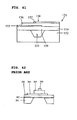
- Fig. 42 is a sectional view showing the structure of a conventional piezoelectric resonator (see, for example, Japanese Unexamined Patent Application Publication No. 2001-279438).
- This piezoelectric resonator includes a substrate 201, a plurality of substrate films 202 and 203, a pair of electrodes 204 and 206, and a piezoelectric thin film 205. Since the substrate film is defined by a plurality of layers as described above, each substrate film shares functions, for example, chemical stability and adhesiveness, and as a result, improvement of the performance and reliability of the piezoelectric resonator are achieved.
- some piezoelectric resonators include piezoelectric vibration portions in which a piezoelectric thin film is sandwiched between opposed upper and lower electrodes, and a high-frequency signal is applied to the sandwiched piezoelectric thin film via the electrodes and, therefore, the piezoelectric thin film vibrates in a thickness vibration mode.
- Examples of such piezoelectric resonators include a diaphragm type piezoelectric resonator having a structure in which an opening of a substrate is covered with a diaphragm made of laminated thin films, and the piezoelectric vibration portion is supported by this diaphragm.
- the residual stress during diaphragm formation is adjusted to be nearly zero and, thereby, the resonant characteristics are improved, or the diaphragm surface is flattened with high precision and, thereby, the resonant characteristics are improved (see, for example, Japanese Unexamined Patent Application Publication No. 2000-244030).
- Japanese Unexamined Patent Application Publication No. 2001-279438 discloses an example of a piezoelectric resonator in which the lower substrate film 202 of a plurality of substrate films is made of SiNx, the upper substrate film is made of Al 2 O 3 , and the piezoelectric thin film is made of ZnO.
- the piezoelectric resonator in which the residual stress during diaphragm formation is adjusted to be nearly zero when the diaphragm surface is not flat, the crystallinity and orientation property of the piezoelectric vibration portion are reduced and, therefore, the resonant characteristics cannot be sufficiently improved.
- the piezoelectric resonator in which the diaphragm surface is flattened when the stress remains, the resonant characteristics cannot be sufficiently improved.
- preferred embodiments of the present invention provide a piezoelectric resonator having a stabilized temperature characteristic of resonant frequency, a method for manufacturing such a novel piezoelectric resonator, a piezoelectric filter including the novel piezoelectric resonator, a duplexer, and a communication apparatus.
- preferred embodiments of the present invention provide a piezoelectric resonator having reduced residual stress in a diaphragm and improved flatness of the diaphragm surface and, therefore, having outstanding resonant characteristics.
- a piezoelectric resonator includes a substrate and a vibration portion provided on the substrate, the vibration portion having a structure in which top and bottom surfaces of a thin film portion including at least one layer of piezoelectric thin film are sandwiched between at least a pair of upper and lower electrodes facing each other in the thickness direction, wherein first and second insulation films are arranged between the substrate and the vibration portion, and the temperature coefficient of resonant frequency of one of the first insulation film, the second insulation film, and the piezoelectric thin film and the temperature coefficients of resonant frequencies of the others have opposite signs.
- the first and second insulation films and the piezoelectric thin film are defined by the film having a positive temperature coefficient of resonant frequency and the film having a negative temperature coefficient of resonant frequency, by setting the film thickness ratio thereof at a proper value, the temperature coefficient of resonant frequency is reduced and, therefore, the frequency temperature characteristic of the entire piezoelectric resonator is stabilized.
- one of the first and second insulation films primarily includes Al 2 O 3 or SiO 2 , or the first insulation film primarily includes Al 2 O 3 and the second insulation film primarily includes SiO 2 .
- the insulation film primarily including SiO 2 is subject to a compressive stress while the insulation film primarily including Al 2 O 3 is subject to a tensile stress, the stress of the entire piezoelectric resonator is controlled, and since Al 2 O 3 has a high thermal conductivity and outstanding exoergic compared with those of SiO 2 , etc., the temperature increase of an element due to an input electric power can be reduced and, therefore, outstanding electric-power resistance can be achieved.
- the arithmetic average surface roughness (Ra) of the lower electrode is preferably about 2.5 nm or less. With this arithmetic average the piezoelectric resonator achieves a Q of at least about 200.
- the arithmetic average surface roughness (Ra) is defined by the stipulation of JIS B0601-2001.
- the upper layer of the first and second insulation films primarily includes Al 2 O 3 , and the arithmetic average surface roughness (Ra) thereof is about 1.0 nm or less.
- the arithmetic average surface roughness (Ra) of the lower electrode provided on the upper layer insulation film is preferably about 2.5 nm or less, and the piezoelectric resonator achieves a Q of at least about 200.
- the upper layer of the first and second insulation films primarily includes Al 2 O 3 , and the stress therein is between about 250 MPa and about 400 MPa on a tensile stress basis. According to this feature, since film formation of the lower electrode provided on the upper layer insulation film is performed with outstanding orientation properties, a piezoelectric resonator having outstanding resonant characteristics is produced.
- the upper layer of the first and second insulation films primarily includes SiO 2 , and the arithmetic average surface roughness (Ra) thereof is about 1.0 nm or less.
- the arithmetic average surface roughness (Ra) of the lower electrode provided on the upper layer insulation film is preferably about 2.5 nm or less, and the piezoelectric resonator achieves a Q of at least about 200.
- the upper layer of the first and second insulation films primarily includes SiO 2 , and the stress therein is about 250 MPa or less on a compressive stress basis. According to this feature, since film formation of the lower electrode provided on the upper layer insulation film is performed with outstanding orientation properties, a piezoelectric resonator having outstanding resonant characteristics is produced.
- the first insulation film is arranged as the upper layer
- the second insulation film is arranged as the lower layer
- the film thickness ratio of piezoelectric thin film / is about 0.7 to about 1.2
- the film thickness ratio of the second insulation film / the first insulation film is between about 1 and about 3.
- the first insulation film is arranged as the lower layer
- the second insulation film is arranged as the upper layer
- the film thickness ratio of piezoelectric thin film / is about 0.7 to about 1.2
- the film thickness ratio of the second insulation film / the first insulation film is between about 1 and about 3.
- an anti-oxidation film is provided on the lower electrode.
- the anti-oxidation film is made of a metal primarily including any one selected from the group consisting of Au, Ru, Rh, Pd, Os, Ir, and Pt.
- the lower electrode is made of a metal primarily including any one selected from the group consisting of Al, Ni, Fe, Mn, Cu, Ti, Mo, W, Ta, and Ag.
- the anti-oxidation film is made of a metal primarily including Au
- the lower electrode is made of a metal primarily including Al
- a diffusion prevention film is arranged between the anti-oxidation film and the lower electrode.
- the diffusion prevention film is made of a metal primarily including any one selected from the group consisting of Ag, Ru, Rh, Pd, Os, Ir, Pt, Mo, and Ti.
- Al 2 O 3 in the first or second insulation film has an oxygen defect.
- Al 2 O 3 in the first or second insulation film has oxygen defect, and the value of defect is within the range of about 0.05 ⁇ x ⁇ about 0.5 in terms of Al 2 O 3-x .
- Al 2 O 3 has a negative temperature-coefficient, when Al 2 O 3 in the insulation film is configured to have an oxygen defect as described above, Al 2 O 3 has a positive temperature coefficient caused by the oxygen defect.
- Al 2 O 3 in the first or second insulation film is in an amorphous state.
- Al 2 O 3 has a negative temperature coefficient, since Al 2 O 3 is in an amorphous state as described above, Al 2 O 3 has a positive temperature coefficient.
- the piezoelectric thin film primarily includes ZnO or AlN. According to this feature, an outstanding frequency temperature characteristic is achieved by combining the first and second insulation films with the piezoelectric thin film primarily including ZnO or AlN.
- the substrate has an opening or a concavity, and the vibration portion is arranged on the opening or concavity.
- the piezoelectric resonator provided with the vibration portion on the opening or concavity of the substrate has a greatly reduced temperature coefficient of resonant frequency and, therefore, the frequency temperature characteristics are stabilized.
- a piezoelectric filter, duplexer, and communication apparatus include the piezoelectric resonator according to preferred embodiments of the present invention. According to this feature, the piezoelectric filter, duplexer, and communication apparatus according to preferred embodiments of the present invention have outstanding frequency temperature characteristics and resonant characteristics.
- a method according to another preferred embodiment for manufacturing a piezoelectric resonator including a substrate, first and second insulation films provided on the substrate, and a structure which is provided on the first and second insulation films and in which top and bottom surfaces of a thin film portion including at least one layer of piezoelectric thin film are sandwiched between at least a pair of upper and lower electrodes facing each other in the thickness direction includes the step of forming an insulation film primarily including Al 2 O 3 by a vacuum evaporation method while the pressure in a film formation apparatus before the start of film formation is less than about 3.0 ⁇ 10 -4 Pa, wherein the insulation film primarily including Al 2 O 3 is the upper layer of the first and second insulation films. According to this method, a piezoelectric resonator having an outstanding frequency temperature characteristic is efficiently manufactured.
- Another method for manufacturing a piezoelectric resonator including a substrate, first and second insulation films provided on the substrate, and a structure which is provided on the first and second insulation films and in which top and bottom surfaces of a thin film portion including at least one layer of piezoelectric thin film are sandwiched between at least a pair of upper and lower electrodes facing each other in the thickness direction includes the step of forming an insulation film primarily including Al 2 O 3 by an electron beam evaporation method at a film thickness growth rate of about 0.6 nm/sec to about 1.0 nm/sec, wherein the insulation film primarily including Al 2 O 3 is the upper layer of the first and second insulation films. According to this method, a piezoelectric resonator having an outstanding frequency temperature characteristic is efficiently manufactured.
- a further method according to another preferred embodiment of the present invention for manufacturing a piezoelectric resonator including a substrate, first and second insulation films provided on the substrate, and a structure which is provided on the first and second insulation films and in which top and bottom surfaces of a thin film portion including at least one layer of piezoelectric thin film are sandwiched between at least a pair of upper and lower electrodes facing each other in the thickness direction includes the step of forming an insulation film primarily including SiO 2 by an RF magnetron sputtering method while the power density is within the range of about 2.0 W/cm 2 to about 8.5 W/cm 2 , wherein the insulation film primarily including SiO 2 is the upper layer of the first and second insulation films.
- the gas pressure during film formation by the RF magnetron sputtering method is preferably about 0.6 Pa or less. According to this method, a piezoelectric resonator having an outstanding frequency temperature characteristic is efficiently manufactured.
- a piezoelectric resonator includes a substrate, an insulation film provided on the substrate, and a vibration portion which is provided on the insulation film, the vibration portion having a structure in which top and bottom surfaces of a thin film portion including at least one layer of piezoelectric thin film are sandwiched between at least a pair of upper and lower electrodes facing each other in the thickness direction, wherein the arithmetic average surface roughness (Ra) of the lower electrode is about 2.5 nm or less.
- the average surface roughness (Ra) on an arithmetic average surface roughness basis is defined by the stipulation of JIS B0601-2001.
- the lower electrode since the arithmetic average surface roughness (Ra) of the lower electrode is about 2.5 nm or less, the lower electrode has greatly improved flatness. Consequently, film formation of the piezoelectric vibration portion located on the insulation film is performed with outstanding crystallinity and orientation properties and, therefore, outstanding resonant characteristics are achieved.
- Ra arithmetic average surface roughness
- the surface of the insulation film has an arithmetic average surface roughness (Ra) of about 1.0 nm or less
- the stress in the insulation film is preferably about 250 MPa or less on a compressive stress basis and about 400 MPa or less on a tensile stress basis.
- the flatness of the lower electrode is further improved, film formation of the piezoelectric vibration portion formed on the insulation film is performed with outstanding crystallinity and orientation properties and, therefore, further improved resonant characteristics are achieved.
- the stress in the insulation film is small, breakage of the insulation film itself and breakage of the piezoelectric vibration portion due to the stress is eliminated. Consequently, since degradation of characteristics and failure of the vibration portion being warped due to the stress is prevented and, in addition, breakage of the vibration portion due to the stress is prevented, and thus, the conforming item rate of the piezoelectric resonators is greatly improved.
- the insulation film primarily includes Al 2 O 3 , and the arithmetic average surface roughness (Ra) thereof is about 1.0 nm or less.
- the insulation film primarily includes Al 2 O 3 , and the stress therein is 250 MPa or more, but 400 MPa or less on a tensile stress basis.
- the insulation film primarily includes SiO 2 , and the arithmetic average surface roughness (Ra) thereof is about 1.0 nm or less.
- the insulation film primarily includes SiO 2 , and the stress therein is about 250 MPa or less on a compressive stress basis.
- an anti-oxidation film is provided on the lower electrode.
- the anti-oxidation film is made of a metal primarily including any one selected from the group consisting of Au, Ru, Rh, Pd, Os, Ir, and Pt.
- the lower electrode is made of a metal primarily including any one selected from the group consisting of Al, Ni, Fe, Mn, Cu, Ti, Mo, W, Ta, and Ag.
- the anti-oxidation film is made of a metal primarily containing Au
- the lower electrode is made of a metal primarily including Al
- a diffusion prevention film is arranged between the anti-oxidation film and the lower electrode.
- This diffusion prevention film is preferably made of a metal primarily containing any one selected from the group consisting of Ag, Ru, Rh, Pd, Os, Ir, Pt, Mo, and Ti.
- the substrate includes an opening or a concavity, and the vibration portion is arranged on the opening or concavity.
- the surface of the insulation film preferably has an arithmetic average surface roughness (Ra) of about 0.7 nm or less, and optimally, has an arithmetic average surface roughness (Ra) of about 0.4 nm or less.
- the stress in the insulation film is preferably about 200 MPa or less on a compressive stress basis, and optimally, about 170 MPa or less.
- a piezoelectric filter according to preferred embodiments of the present invention is provided with the piezoelectric resonator according to preferred embodiments of the present invention as a filter element.
- Another piezoelectric filter according to preferred embodiments of the present invention is provided with a plurality of piezoelectric resonators according to preferred embodiments of the present invention as filter elements, and these filter elements are connected so as to have a ladder type configuration.
- a duplexer according to preferred embodiments of the present invention is provided with the piezoelectric resonator according to preferred embodiments of the present invention.
- another duplexer according to preferred embodiments of the present invention is provided with the piezoelectric filter according to preferred embodiments of the present invention.
- the piezoelectric filter and duplexer according to preferred embodiments of the present invention is provided with the piezoelectric resonator having outstanding characteristics and, therefore, when adopted for communication apparatuses, outstanding performance is achieved regarding the functions as a filter and switching of signals.
- Yet another method according to another preferred embodiment of the present invention for manufacturing a piezoelectric resonator including a substrate, an insulation film provided on the substrate, and a vibration portion provided on the insulation film, the vibration portion having a structure in which top and bottom surfaces of a thin film portion including at least one layer of piezoelectric thin film are sandwiched between at least a pair of upper and lower electrodes facing each other in the thickness direction includes a step of forming the insulation film from silicon oxide as a primary component by an RF magnetron sputtering method while the power density is within the range of about 2.0 W/cm 2 to about 8.5 W/cm 2 and forming the piezoelectric thin film from zinc oxide as a primary component.
- the insulation film is formed by the RF magnetron sputtering method in the condition that the power density thereof is large, the stress is adjusted to be small, and film formation is performed with outstanding flatness of the surface.
- the gas pressure during film formation by the RF magnetron sputtering method is preferably about 0.6 Pa or less.
- the gas pressure refers to a gas pressure in a film formation apparatus when film formation is performed by the RF magnetron sputtering method.
- a dense and smooth film that is, a film having a small arithmetic average surface roughness (Ra) is formed.
- a further method according to another preferred embodiment of the present invention for manufacturing a piezoelectric resonator including a substrate, first and second insulation films provided on the substrate, and a vibration portion provided on the first and second insulation films, the vibration portion having a structure in which top and bottom surfaces of a thin film portion including at least one layer of piezoelectric thin film are sandwiched between at least a pair of upper and lower electrodes facing each other in the thickness direction, includes the step of forming an insulation film primarily including Al 2 O 3 by a vacuum evaporation method while the pressure in a film formation apparatus before the start of film formation is preferably less than about 3.0 ⁇ 10 -4 Pa, wherein the insulation film primarily including Al 2 O 3 is the upper layer of the first and second insulation films.
- the surface of the insulation film is flattened and, in addition, the stress is greatly reduced.
- Another method for manufacturing a piezoelectric resonator including a substrate, an insulation film provided on the substrate, and a vibration portion provided on the insulation film, the vibration portion having a structure in which top and bottom surfaces of a thin film portion including at least one layer of piezoelectric thin film are sandwiched between at least a pair of upper and lower electrodes facing each other in the thickness direction includes the first step of forming the insulation film from aluminum oxide as a primary component by an electron beam evaporation method at a film thickness growth rate within the range of about 0.6 m/sec to about 1.0 nm/sec and the second step of forming the piezoelectric thin film from zinc oxide as a primary component.
- the surface of the insulation film is flattened and, in addition, the stress is greatly reduced.
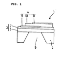
- Fig. 1 is a sectional view showing the structure of a piezoelectric resonator according to a preferred embodiment of the present invention.
- the piezoelectric resonator 1 of the present preferred embodiment is provided with a substrate 2, insulation thin film 3, and piezoelectric element portion 4.
- the substrate 2 is made of silicon, for example, and has an opening 5 penetrating the top and bottom surfaces corresponding to a vibration portion.
- the insulation thin film 3 is arranged on the substrate 2 while covering the opening 5, and has a SiO 2 film 6 primarily including SiO 2 as a first insulation thin film and an Al 2 O 3 film 7 primarily including Al 2 O 3 as a second insulation thin film.
- the piezoelectric element portion 4 is defined by a piezoelectric thin film 10 which primarily includes ZnO and which is sandwiched between a pair of upper and lower electrodes 8 and 9.
- the piezoelectric resonator 1 of the present preferred embodiment is provided with the SiO 2 film 6, Al 2 O 3 film 7, and the piezoelectric thin film 10 primarily including ZnO. Since SiO 2 has a positive temperature coefficient, Al 2 O 3 has a negative temperature coefficient, and ZnO has a negative temperature coefficient, the temperature coefficient of resonant frequency is reduced to close to zero and, therefore, the temperature coefficient of resonant frequency is stabilized by properly setting the film thickness ratio among them.
- the stress in the Al 2 O 3 film 7 is a tensile stress of between about 250 MPa and about 400 MPa.
- Table 1 shows the relationship between the film thickness ratio and the frequency temperature characteristic of this piezoelectric resonator 1.
- T ZnO /T Al2O3 /T SiO2 indicates the film thickness ratio of the piezoelectric thin film 10, Al 2 O 3 film 7, and SiO 2 film 6.
- Table 2 shows the relationship between the film thickness ratio and the resonant characteristics of this piezoelectric resonator 1.
- each of the characteristics Q, k 2 , and Q ⁇ k 2 is shown with respect to the film thickness ratio of the piezoelectric thin film 10, Al 2 O 3 film 7, and SiO 2 film 6, T ZnO /T Al2O3 /T SiO2 .
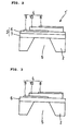
- the characteristics with respect to the film thickness ratio of the piezoelectric thin film 10, SiO 2 film 6, and Al 2 O 3 film 7, T ZnO /T SiO2 /T Al2O3 , in a piezoelectric resonator 1' of another preferred embodiment of the present invention are shown, wherein as shown in Fig.
- the constituent materials of the first and second insulation thin films are interchanged, that is, the first insulation thin film is specified to be the Al 2 O 3 film 7 primarily including Al 2 O 3 , and the second insulation thin film is specified to be the SiO 2 film 6 primarily including SiO 2 and, in addition, for purposes of comparison, the characteristics with respect to the two-layer structure of ZnO and SiO 2 without formation of Al 2 O 3 as shown in Fig. 3 are shown.
- the stress in the SiO 2 film 6 is a compressive stress of about 250 MPa or less.
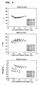
- Fig. 4 and Fig. 5 show characteristics of the resonator when the film thickness is changed based on a simulation performed by the inventors of the present invention.
- Fig. 4 shows the results with respect to the structure of upper electrode / ZnO / lower electrode / SiO 2 / Al 2 O 3
- Fig. 5 shows the results with respect to the structure of upper electrode / ZnO / lower electrode / Al 2 O 3 / SiO 2 .
- the calculation is performed based on the assumption that the upper and lower electrodes sandwiching ZnO are made of Al and the film thicknesses are fixed at about 180 nm.
- Each drawing shows the calculation result when the film thickness ratio of SiO 2 to Al 2 O 3 is changed from 3:1 to 1:3 in five steps while the axis of abscissas indicates the film thickness ratio of ZnO/(SiO 2 + Al 2 O 3 ).
- the graph in the upper column indicates the relationship between the film thickness ratio and Q
- the graph in the middle column indicates the relationship between the film thickness ratio and k 2
- the graph in the lower column indicates the relationship between the film thickness ratio and frequency temperature characteristic (TCF).
- TCF frequency temperature characteristic
- the structure of upper electrode / ZnO / lower electrode / SiO 2 / Al 2 O 3 has the k 2 greater than that of the structure of upper electrode / ZnO / lower electrode / Al 2 O 3 / SiO 2 .
- the acoustic impedance of SiO 2 is about 1.3 ⁇ 10 7 (N ⁇ s/m 3 ), and is less than about 3.5 ⁇ 10 7 (N ⁇ s/m 3 ) of ZnO and about 3.9 ⁇ 10 7 (N ⁇ s/m 3 ) of Al 2 O 3 (wherein the value of Al 2 O 3 is the value of a single crystal (sapphire), and the practical value is estimated to be about 2.3 ⁇ 10 7 (N ⁇ s/m 3 ).
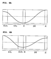
- Figs. 6A and 6B show displacement diagrams of vibration, and it is clear that the displacement in ZnO is greater than the displacement in SiO 2 .
- the axis of abscissas indicates the vibration portion while the thickness widths of the insulation film, piezoelectric film, and electrode film in the thickness direction correspond to the horizontal widths, and the axis of ordinates indicates the displacement of vibration.
- FIG. 6A shows the situation where the lower layer of the insulation film is an Al 2 O 3 film and the upper layer of the insulation film is a SiO 2 film.
- Fig. 6B shows the situation where the lower layer of the insulation film is a SiO 2 film and the upper layer of the insulation film is an Al 2 O 3 film.
- the structure of upper electrode /ZnO / lower electrode / Al 2 O 3 / SiO 2 has the absolute value of the TCF (temperature change rate of frequency) that is less than that of the structure of upper electrode / ZnO /lower electrode / SiO 2 / Al 2 O 3 .
- the temperature coefficients of the materials of ZnO and Al 2 O 3 are negative (frequency decreases with increase in temperature), while that of SiO 2 is positive. Consequently, as is clear from Figs. 6A and 6B, the structure of ZnO / Al 2 O 3 / SiO 2 exhibiting large displacement in SiO 2 is significantly affected by the temperature coefficient of SiO 2 and, therefore, the total temperature coefficient shifts in the positive direction (approaches zero).
- the film thickness ratio of ZnO/(SiO 2 + Al 2 O 3 ) is about 0.7 to about 1.2 from the standpoint of an increase in k 2 , while the ratio is about 0.6 to about 0.8 from the standpoint of an increase in Q.
- the film thickness ratio of SiO 2 : Al 2 O 3 is preferably at least about 1.
- the film thickness ratio of SiO 2 : Al 2 O 3 is preferably between about 1 and about 3.
- the film thickness ratio of SiO 2 : Al 2 O 3 is preferably about 1 or more from the standpoint of reduction of the TCF.
- the dependence on the film thickness of ZnO is small, and the effectiveness is verified in the entire range checked at this time. Consequently, the film thickness ratio of ZnO/(SiO 2 + Al 2 O 3 ) is about 0.7 to about 1.2, and the film thickness ratio of SiO 2 : Al 2 O 3 is at least about 1.
- the film thickness ratio of SiO 2 : Al 2 O 3 is preferably between about 1 and about 3.
- the SiO 2 film 6 is formed on the top surface of the substrate 2 by a thermal oxidation method, sputtering method, or other suitable method.
- the opening 5 is formed with respect to the bottom surface of the substrate 2 by anisotropic etching, RIE (Reactive Ion Etching), or other suitable method.
- the Al 2 O 3 film 7 is formed on the SiO 2 film 6 by a film forming method, for example, an electron beam evaporation method and sputtering method.
- film formation of the Al 2 O 3 film 7 is performed by the electron beam evaporation method using aluminum oxide as an evaporation source at a film growth rate of about 0.8 nm/sec or less.
- the lower layer electrode 9 is formed on this Al 2 O 3 film 7 by evaporation, sputtering, or other suitable method.
- the film growth rate of the Al 2 O 3 film 7 is preferably about nm/sec 0.6 to about 1.0 nm/sec to improve manufacturing efficiency.
- the piezoelectric thin film 10 primarily including ZnO is formed on the lower layer electrode 9 and the Al 2 O 3 film 7 by a film formation method, for example, sputtering and CVD.
- a film formation method for example, sputtering and CVD.
- a highly oriented film is manufactured by an RF sputtering method using a ZnO target at a substrate temperature of about 50°C to about 500°C, an RF power of about 300 W to about 1,500 W, and a gas pressure of about 0.05 Pa to about 0.8 Pa.
- the upper layer electrode 8 is formed on this piezoelectric thin film 10 in a similar manner to that for the lower layer electrode 9.
- both the piezoelectric thin film 10 primarily including ZnO and the SiO 2 film 6 are subject to a compressive stress while the Al 2 O 3 film 7 is subject to a tensile stress, the stress in the total piezoelectric thin film resonator 1 is greatly reduced and, therefore, failures due to cracking of the element are greatly reduced.
- Al 2 O 3 has a negative temperature coefficient as described above.
- Al 2 O 3 has oxygen defect and is in an amorphous state
- Al 2 O 3 has a positive temperature coefficient. Consequently, in another preferred embodiment of the present invention, by providing Al 2 O 3 with oxygen defect, for example, by providing Al 2 O 3 in the amorphous state, the Al 2 O 3 film has a positive temperature coefficient, and can be combined with the piezoelectric thin film primarily including ZnO and having a negative temperature coefficient so as to achieve an outstanding frequency temperature characteristic.
- the value of defect is preferably within the range of about 0.05 ⁇ x ⁇ about 0.5 in terms of Al 2 O 3-x .
- the insulation thin film 3 and the piezoelectric element portion 4 are disposed on the opening 5 of the substrate 2.
- the insulation thin film 3 and the piezoelectric element portion 4 may be disposed on a concavity 5' of the substrate 2 as shown in Fig. 7.
- Fig. 8 and Fig. 9 show the measurement results of the experiments performed by the inventors of the present invention
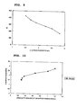
- Fig. 8 shows the relationship between the surface roughness of the lower electrode and the rocking curve half-width of the piezoelectric thin film
- Fig. 9 shows the relationship between the surface roughness of the lower electrode and the Q.
- the Q required for a resonator used for a ladder filter is at least about 200, and as shown in Fig.
- the Q of the resonator is at least about 200. Consequently, in order to produce the resonator having a Q of at least about 200 suitable for defining the ladder filter, the arithmetic average surface roughness (Ra) of the lower electrode must be about 2.5 nm or less.
- the arithmetic average surface roughness (Ra) of an insulation film to become a substrate thereof must be small.
- Fig. 10 shows the measurement results of the experiments performed by the inventors of the present invention
- the arithmetic average surface roughness (Ra) of the upper layer insulation film is about 1.0 nm or less
- the arithmetic average surface roughness (Ra) of the lower electrode arranged thereon is about 2.5 nm or less.
- the arithmetic average surface roughness (Ra) of the insulation film is set to about 1.0 nm or less, the lower electrode having an arithmetic average surface roughness (Ra) of about 2.5 nm or less is produced, the piezoelectric thin film having high orientation property is produced and, by extension, the resonator having a Q of at least about 200 suitable for defining the ladder filter is produced.
- the inventors of the present invention performed research regarding a film formation method for the insulation film of Al 2 O 3 having the arithmetic average surface roughness (Ra) of about 1.0 nm or less.
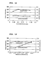
- the inventors of the present invention formed films by an electron beam evaporation method while only the individual film formation rates were differentiated and other condition were maintained substantially the same and, thereby, the results as shown in Fig. 11 were obtained. As is clear from Fig. 11, it was verified that the film formation rate did not substantially affect the stress and surface roughness of the resulting insulation film.
- Fig. 11 it was verified that the film formation rate did not substantially affect the stress and surface roughness of the resulting insulation film.
- 11 is a graph showing the relationship between the film formation rate and the tensile stress and the relationship between the film formation rate and the surface roughness while the axis of abscissas indicates the film formation rate, and the axis of ordinates indicates the tensile stress and the surface roughness.
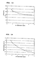
- the inventors of the present invention formed films by an electron beam evaporation method as an example of the same vacuum evaporation method while only the individual pressures in the film formation apparatus before starting film formation were differentiated and other conditions were not changed, for example, all of the film formation rates were about 0.8 nm/sec, and thereby, the results as shown in Fig. 12 were obtained.
- the insulation film having an arithmetic average surface roughness (Ra) of about 1.0 nm or less were produced.
- FIG. 12 is a graph showing the relationship between the degree of vacuum in the apparatus and the tensile stress and the relationship between the film formation rate and the surface roughness while the axis of abscissas indicates the degree of vacuum on a pressure basis in the apparatus when the vacuum evaporation is performed, and the axis of ordinates indicates the tensile stress and the surface roughness.
- the pressure in the film formation apparatus is affected by the impurities floating in the film formation apparatus. Consequently, when the impurities floating in the film formation apparatus are reduced to the extent that the pressure in the film formation apparatus before the start of film formation is less than about 3.0 ⁇ 10 -4 Pa, the insulation film having a high purity and an arithmetic average surface roughness (Ra) of about 1.0 nm or less is produced.
- the Al 2 O 3 film 7 as the upper layer insulation film is formed on the lower layer insulation film 6 made of SiO 2 and arranged on the top surface of the substrate 2 made of a silicon wafer by an electron beam evaporation method at a film thickness growth rate within the range of about 0.6 (nm/sec) to about 1.0 (nm/sec).
- the surface roughness of the Al 2 O 3 film 7 formed by the film formation method is about 0.6 nm on an arithmetic average surface roughness (Ra) basis.
- the stress in this Al 2 O 3 film 7 is a tensile stress of about 300 MPa.
- the lower layer of the insulation film is an Al 2 O 3 film
- a film formation method in which a film of SiO 2 is formed on the Al 2 O 3 film will be explained with reference numerals based on the piezoelectric resonator shown in Fig. 2.
- the insulation film 6 primarily including SiO 2 is formed by an RF magnetron sputtering method on the lower layer insulation film 7 made of Al 2 O 3 arranged on the top surface of the substrate 2 made of a silicon wafer.
- the gas pressure is preferably within the range of about 0.1 to about 0.25 Pa, and the power density is within the range of about 2.0 W/cm 2 to about 8.5 W/cm 2 . It is very desirable that the gas pressure during film formation is about 0.6 Pa or less.
- the surface roughness of the SiO 2 film 6 formed by the film formation method is about 0.3 nm on an arithmetic average surface roughness (Ra) basis.
- the stress in this insulation film 6 of the piezoelectric resonator 1 is a compressive stress of about 150 MPa. When the tensile stress is assumed to be a positive value, this compressive stress has a negative value and, therefore, is about -150 MPa.
- the stress in the SiO 2 film 6 formed as described above is preferably about 250 MPa or less.
- the surface roughness of the surface of the insulation film is about 1.0 nm or less on an arithmetic average surface roughness (Ra) basis, and the stress therein is reduced in the range of about 250 MPa or less on a compressive stress basis. The reasons for this will be described.
- the relationship between the film formation pressure (pressure of the gas) and the stress has been known. That is, it is a known relationship that when the film formation pressure (pressure of the gas) is increased, the compressive stress is reduced, and when the film formation pressure (pressure of the gas) is reduced, the compressive stress is increased. Therefore, in order to reduce the compressive stress, the film formation pressure (pressure of the gas) is set at a high level. However, when the film formation pressure (pressure of the gas) is set at a high level, the surface roughness of the resulting insulation film becomes coarse and, therefore, it is difficult to allow reduction of surface roughness and reduction of stress to become mutually compatible.
- Examples of conventional film formation methods for insulation films of SiO 2 include a thermal oxidation method, low pressure CVD method, sol-gel process, and evaporation method.
- the stress is increased when film formation is performed by each and every method.
- the stress is increased to about 300 MPa to about 400 MPa in the case of the thermal oxidation method, and to several hundreds of megapascals in the evaporation method.
- One of the reasons for the increase of stress in these methods is that the temperature during film formation is high. The temperature is about 300°C in the sputtering method, whereas the temperature is about 500°C to about 800°C in the low pressure CVD method, and is about 1,100°C in the thermal oxidation method. Therefore, the sputtering method produces less thermal stress.
- the thermal oxidation method cubical expansion of the surface of the film due to O 2 is brought about and, as a result, the stress is increased.
- the firing temperature is high and, in addition, variations in the film thickness are likely to occur due to a property specific to this sol-gel process. Consequently, the film surface has poor flatness.
- an insulation film that is subjected to a reduced stress and having an arithmetic average surface roughness of the film surface of about 1.0 nm or less is formed by adjusting the RF power density. Furthermore, when the power of the RF magnetron sputtering is increased, defects in the film are reduced and, therefore, a dense film is produced. As is clear from Fig.
- the RF power density is increased to more than about 8.5 (W/cm 2 ), a target becomes likely to crack and, therefore, film formation is adversely affected. Consequently, the RF power density is preferably set to about 8.5 (W/cm 2 ) or less.
- Fig. 15 shows that the Q as a resonant characteristic is improved with increases in the RF power density.
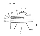
- the anti-oxidation film 9a is made of a metal, for example, Au, Ru, Rh, Pd, Os, Ir, and Pt, that is unlikely to oxidize. It is essential that the anti-oxidation film 9a has a thickness that is adequate to prevent oxidation of the lower electrode 9, and the thickness required is about 4 nm to about 30 nm.
- the anti-oxidation film 9a is formed on the smooth lower electrode 9 and, therefore, becomes a smooth film similar to the lower electrode 9. Consequently, the piezoelectric thin film 10 arranged on the anti-oxidation film 9a has outstanding orientation properties.
- the diffusion prevention film 9b is made of a metal primarily including any one selected from the group consisting of Ag, Ru, Rh, Pd, Os, Ir, Pt, Mo, and Ti, and it is essential that the diffusion prevention film 9b has a thickness that is adequate to prevent mutual diffusion between Au and Al, and the required thickness is about 4 nm to about 30 nm.
- the piezoelectric resonator of various preferred embodiments of the present invention can be incorporated into a ⁇ type, L type, and T type ladder filters shown in Figs. 18A, 18B, and 18C, respectively, and outstanding filter characteristics are achieved.
- the piezoelectric resonator according to preferred embodiments of the present invention may be used for a duplexer 11 as shown in Fig. 19, and furthermore, may be mounted on a cellular phone and other communication apparatuses, and may be used for electronic communication operations such that the operation characteristics thereof are stabilized.
- This piezoelectric resonator 101 includes a substrate 102, opening 103, insulation film 104, lower electrode 105, piezoelectric thin film 106, and upper electrode 107.
- the substrate 102 is made of a semiconductor substrate, for example, a silicon wafer.
- the opening 103 is formed by, for example, anisotropic etching, with respect to the bottom surface side of the substrate 102.
- the insulation film 104 is a film which is formed from, for example, silicon oxide (SiO 2 ), on the top surface side of the substrate 102 and which has an electrically insulating property.
- the lower electrode 105 is a film formed on the insulation film 104 from an appropriate electrode material, for example, aluminum, into a predetermined pattern.
- the piezoelectric thin film 106 is a piezoelectric film formed on the top surface of a portion of the lower electrode 105 and insulation film 104 from, for example, zinc oxide (ZnO) as a primary component.
- the upper electrode 107 is a film formed on the piezoelectric thin film 106 from an appropriate electrode material, for example, aluminum, into a predetermined pattern.
- the lower electrode 105 and the upper electrode 107 are configured to sandwich the piezoelectric thin film 106 in the condition that a portion of them are facing each other in the thickness direction.
- a piezoelectric vibration portion 108 is defined by the lower electrode 105, upper electrode 107, and piezoelectric thin film 106 as described above.
- the piezoelectric vibration portion 108 is configured so as to vibrate in a thickness longitudinal vibration mode by, for example, a high-frequency electric signal applied to the lower electrode 105 and the upper electrode 107.
- the insulation film 104 covering the opening 103 defines a diaphragm 109 and supports the piezoelectric vibration portion 108.
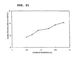
- arithmetic average surface roughness (Ra) of the lower electrode when the arithmetic average surface roughness (Ra) of the lower electrode is reduced, the orientation property of the piezoelectric film arranged thereon is improved and, therefore, outstanding resonant characteristics are achieved.
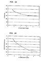
- the Q required for a resonator used for a ladder filter is at least about 200, and as shown in Fig. 22, when the arithmetic average surface roughness (Ra) of the lower electrode is about 2.5 nm or less, the Q of the resonator is about 200 or more. Consequently, in order to produce the resonator having a Q of at least about 200 suitable for defining the ladder filter, the arithmetic average surface roughness (Ra) of the lower electrode must be about 2.5 nm or less.
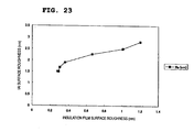
- the arithmetic average surface roughness (Ra) of an insulation film defining a substrate thereof must be small.
- the arithmetic average surface roughness (Ra) of the insulation film is about 1.0 nm or less
- the arithmetic average surface roughness (Ra) of the lower electrode arranged thereon is about 2.5 nm or less.
- the arithmetic average surface roughness (Ra) of the insulation film is set to be about 1.0 nm or less, the lower electrode having an arithmetic average surface roughness (Ra) of about 2.5 nm or less is produced, the piezoelectric thin film having high orientation properties is produced and, by extension, the resonator having a Q of at least about 200 suitable for defining the ladder filter is produced.
- FIG. 24A the substrate 2 made of a silicon wafer is prepared.
- the insulation film 104 primarily including silicon oxide (SiO 2 ) is formed on the substrate 102 by an RF magnetron sputtering method.
- This film formation step is the first step in the method for manufacturing the piezoelectric resonator including the insulation film primarily including silicon oxide.
- the gas pressure is about 0.1 Pa to about 0.25 Pa, and the power density is about 2.0 W/cm 2 to about 8.5 W/cm 2 .
- a photoresist is patterned on the insulation film 104 by photolithography, and a film of the lower electrode 105 made of aluminum is formed by evaporation, sputtering, or other suitable method, from above this photoresist. After this film formation, the photoresist is lifted off.
- the pressure during film formation of the insulation film 104 is preferably about 0.1 Pa to about 0.25 Pa as described above. However, it is preferably about 0.6 Pa or less.
- the piezoelectric thin film 106 primarily including zinc oxide (ZnO) is formed in the desired range on the insulation film 104 and the lower electrode 105 by sputtering while masking is performed with a metal mask, although not shown in the drawing.
- This film formation step is the second step in the method for manufacturing the piezoelectric resonator including the insulation film primarily including silicon oxide. Subsequently, as shown in Fig.
- a photoresist is patterned on the piezoelectric thin film 106 by photolithography, and a film of the upper electrode 107 made of aluminum (Al) is formed while facing a portion of the lower electrode 105 in the thickness direction by evaporation, sputtering, or other suitable method, from above this photoresist. Subsequently, films of electrode pads, although not shown in the drawing, are formed and, thereafter, the photoresist is lifted off.
- the opening 103 is formed by performing an anisotropic etching treatment with respect to the back side of the substrate 102.
- the opening 103 is formed such that the top surface of the opening 103 extends to the insulation film 104.
- the manufacturing step of the piezoelectric resonator according to preferred embodiments of the present invention is completed through each of the steps.
- the surface roughness of the insulation film 104 of the piezoelectric resonator 101 manufactured through the steps is preferably about 0.3 nm on an arithmetic average surface roughness (Ra) basis.
- the stress in this insulation film 104 of the piezoelectric resonator 101 is a compressive stress of about 150 MPa. When the tensile stress is a positive value, this compressive stress shows a negative value and, therefore, is about -150 MPa.
- the surface roughness of the surface of the insulation film is about 1.0 nm or less on an arithmetic average surface roughness (Ra) basis, and the stress is reduced such that the stress is within the range of about 250 MPa or less on a compressive stress basis.
- the relationship between the film formation pressure (pressure of the gas) and the stress is known. That is, it is a known relationship that when the film formation pressure (pressure of the gas) is increased, the compressive stress is reduced, and when the film formation pressure (pressure of the gas) is reduced, the compressive stress is increased. Therefore, in order to reduce the compressive stress, the film formation pressure (pressure of the gas) is set at a high level. However, when the film formation pressure (pressure of the gas) is set at a high level, the surface roughness of the resulting insulation film increases and, therefore, it is difficult to reduce the surface roughness and reduce of stress to be mutually compatible.
- Examples of conventional film formation methods for insulation films of silicon oxide include a thermal oxidation method, low pressure CVD method, sol-gel process, and evaporation method.
- the stress is increased when film formation is performed by each and every method.
- the stress is increased to about 300 MPa to about 400 MPa in the case of the thermal oxidation method, and to several hundreds of megapascals in the evaporation method.
- One of the reasons for the increase of stress in these methods is that the temperature during film formation is high. The temperature is about 300°C in the sputtering method, whereas the temperature is about 500°C to about 800°C in the low pressure CVD method, and is about 1,100°C in the thermal oxidation method and, therefore, the sputtering method produces less thermal stress.
- the thermal oxidation method cubical expansion of the surface of the film due to O 2 is produced and, as a result, the stress is increased.
- the firing temperature is high and, in addition, variations in the film thickness occur due to a property specific to this sol-gel process. Consequently, the film surface has reduced flatness.
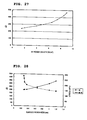
- the insulation film subject to a reduced stress and having an arithmetic average surface roughness of the film surface of about 1.0 nm or less is formed by adjusting the RF power density. Furthermore, when the power of the RF magnetron sputtering is increased, defects in the film are reduced and, therefore, the dense film is produced. As is clear from Fig.
- the RF power density is increased to more than about 8.5 (W/cm 2 ), a target is likely to crack and, therefore, film formation is adversely affected. Consequently, the RF power density is preferably set to about 8.5 (W/cm 2 ) or less.
- Fig. 27 shows that the Q as a resonant characteristic is improved with increases in the RF power density.
- Fig. 28 shows that the Q as a resonant characteristic is improved and the stress in the insulation film is reduced with decreases in the surface roughness.
- the insulation film is a layer of silicon oxide (SiO 2 ) and the piezoelectric thin film of zinc oxide (ZnO) is laminated on the insulation film as in the second preferred embodiment, since both of the insulation film and the piezoelectric thin film have a compressive stress, the stress in the diaphragm 109 and the total piezoelectric vibration portion 108 is reduced when the stress in the insulation film is reduced.
- the inventors of the present invention performed research regarding a film formation method for the insulation film of Al 2 O 3 having an arithmetic average surface roughness (Ra) of about 1.0 nm or less.
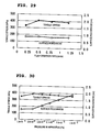
- films were formed by an electron beam evaporation method while only the individual film formation rates were differentiated and other condition were not substantially changed and, thereby, the results as shown in Fig. 29 were obtained. As is clear from Fig. 29, it was verified that the film formation rate does not substantially affect the stress and surface roughness of the resulting insulation film.
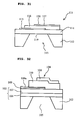
- films were formed by the same electron beam evaporation method while only the individual pressures in the film formation apparatus before the start of film formation were differentiated and other conditions were not substantially changed, for example, all of the film formation rates were about 0.8 nm/sec, and thereby, the results as shown in Fig. 30 were obtained.
- the film formation was performed while the pressure in the film formation apparatus before start of film formation was less than about 3.0 ⁇ 10 -4 Pa, the insulation film having an arithmetic average surface roughness (Ra) of about 1.0 nm or less was produced.
- the pressure in the film formation apparatus is affected by the impurities floating in the film formation apparatus. Since the ratio of impurities floating in the film formation apparatus is reduced with a decrease in the pressure in the film formation apparatus, when the impurities floating in the film formation apparatus are reduced to the degree that the pressure in the film formation apparatus before the start of film formation is less than about 3.0 ⁇ 10 -4 Pa, the insulation film having a high purity and an arithmetic average surface roughness (Ra) of about 1.0 nm or less is produced.
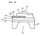
- FIG. 31 is a vertical front view showing the structure of a piezoelectric resonator.
- an insulation film 114 made of aluminum oxide (Al 2 O 3 ), a lower electrode 115 made of aluminum, a piezoelectric thin film 116 primarily including zinc oxide (ZnO), and an upper electrode 117 made of aluminum are arranged sequentially on a silicon substrate 112.
- the lower electrode 115 and the upper electrode 117 are arranged to sandwich the piezoelectric thin film 116 such that a portion of the lower electrode 115 and the upper electrode 117 are facing each other in the thickness direction.
- a piezoelectric vibration portion 118 is defined by the sandwiched portion of this piezoelectric thin film 116 and the lower electrode 115 and upper electrode 117 sandwiching it. This piezoelectric vibration portion 118 is configured to vibrate in a thickness longitudinal vibration mode by an electric signal through the lower electrode 115 and the upper electrode 117.
- An opening 113 is arranged underneath the piezoelectric vibration portion 118 by anisotropic etching or reactive ion etching.
- a portion of the insulation film 114 covering the opening 113 defines a diaphragm 119 supporting this piezoelectric vibration portion 118 such that the piezoelectric vibration portion 118 can vibrate.
- the substrate 112 made of a silicon wafer is prepared.
- the insulation film 114 is formed on the substrate 112 by an electron beam evaporation method at a film thickness growth rate within the range of about 0.6 (nm/sec) to about 1.0 (nm/sec).
- This film formation step is the first step in the method for manufacturing the piezoelectric resonator including the insulation film primarily containing aluminum oxide.
- the lower electrode 115 made of aluminum (Al) is formed on this insulation film 114 by a lift-off evaporation method, or other suitable method. After this film formation, a photoresist is lifted off.
- the piezoelectric thin film 116 primarily including zinc oxide (ZnO) is formed in a predetermined region on the insulation film 114 and the lower electrode 115 by reactive sputtering while masking is performed with a metal mask, although not shown in the drawing.
- This film formation step is the second step in the method for manufacturing the piezoelectric resonator including the insulation film primarily containing aluminum oxide.
- a film of the upper electrode 117 made of aluminum (Al) is formed on the piezoelectric thin film 116, while facing a portion of the lower electrode 115 in the thickness direction by evaporation, sputtering, or other suitable method.
- films of electrode pads although not shown in the drawing, are formed and, thereafter, the photoresist is lifted off.
- the opening 113 is formed by performing an anisotropic etching treatment on the back surface of the substrate 112. In this case, the opening 113 is formed such that the ceiling surface of the opening 113 extends to the insulation film 114.
- the surface roughness of the insulation film 114 of the piezoelectric resonator 111 manufactured by the steps is about 0.6 nm on an arithmetic average surface roughness (Ra) basis.
- the stress in this insulation film 114 of the piezoelectric resonator 111 is a tensile stress of at least about 300 MPa.
- the piezoelectric resonator of the present preferred embodiment since aluminum oxide has a tensile stress in contrast to zinc oxide, the stress of the total element is reduced, the element is unlikely to break and, therefore, reliability is improved. The resonant characteristics of the laminated electrode films, piezoelectric thin film, and piezoelectric resonator are improved.
- the insulation film is a layer of aluminum oxide (Al 2 O 3 ) and the piezoelectric thin film of zinc oxide (ZnO) is laminated on the insulation film as in the third preferred embodiment, since the insulation film has a tensile stress and the piezoelectric thin film has a compressive stress, these stresses are adjusted to cancel each other, the stress in the diaphragm 109 and the total piezoelectric vibration portion 118 is greatly reduced.
- the lower electrode When a metal, for example, Al, likely to be oxidized is used for the lower electrode, Al is oxidized during film formation of the piezoelectric thin film, the surface of the lower electrode becomes aluminum oxide and, therefore, the orientation property of the piezoelectric thin film arranged on the lower electrode is deteriorated. Even when the lower electrode having a small arithmetic average surface roughness (Ra) is formed, degradation of the orientation property of the piezoelectric thin film occurs when the surface of the lower electrode is oxidized. The same is true for the case where the lower electrode made of a metal primarily containing Ni, Fe, Mn, Cu, Ti, Mo, W, Ta, or Ag other than Al.
- Ra arithmetic average surface roughness
- the anti-oxidation film is made of a metal primarily including, for example, Au, Ru, Rh, Pd, Os, Ir, and Pt, that is unlikely to oxidize. It is essential that the anti-oxidation film has a thickness adequate to prevent oxidation of the lower electrode, and the thickness required is about 4 nm to about 30 nm.
- the anti-oxidation film is formed on the smooth lower electrode and, therefore, becomes a smooth film similar to the lower electrode. Consequently, the piezoelectric thin film arranged on the anti-oxidation film has outstanding orientation property.
- the diffusion prevention film is made of a metal primarily including any one selected from the group consisting of Ag, Ru, Rh, Pd, Os, Ir, Pt, Mo, and Ti, and it is essential that the diffusion prevention film has a thickness adequate to prevent mutual diffusion between Au and Al, and the required thickness is about 4 nm to average surface roughness101average surface roughnessaverage surface roughnessaverage surface roughnessaverage surface roughnessaverage surface roughnessaverage surface roughnessaverage surface roughnessabout 30 nm.
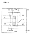
- Fig. 34 to Fig. 36 show a piezoelectric filter including the piezoelectric resonator of the second preferred embodiment of the present invention.
- This piezoelectric filter has a ladder type configuration.
- Fig. 34 is a schematic plan view showing the piezoelectric filter
- Fig. 35 is a sectional view of the section indicated by a line A-A of the piezoelectric filter shown in Fig. 34
- Fig. 36 is a circuit diagram of the piezoelectric filter shown in Fig. 34.
- a piezoelectric filter 121 defined by a L type ladder filter includes a substrate 122 made of a silicon wafer, an opening 123 arranged in the substrate 122, an insulation film made of silicon oxide (SiO 2 ), lower electrodes 125a and 125b made of aluminum, a piezoelectric thin film 126 primarily containing zinc oxide (ZnO), and an upper electrode 127 made of aluminum.
- the lower electrode 125a, the upper electrode 127, and the portion of the piezoelectric thin film 126 sandwiched between the two electrodes 125a and 127 define a piezoelectric vibration portion 128a which is a series piezoelectric resonator.
- the lower electrode 125b, the upper electrode 127, and the portion of the piezoelectric thin film 126 sandwiched between the two electrodes 125b and 127 define a piezoelectric vibration portion 128b which is a parallel piezoelectric resonator.
- the portion of the insulation film 124 covering the opening 123 defines a diaphragm 129 supporting the piezoelectric vibration portions 128a and 128b such that these piezoelectric vibration portions 128a and 128b can vibrate.
- the substrate 122 made of a silicon wafer is prepared.
- the insulation film 124 primarily including silicon oxide (SiO 2 ) is formed on the substrate 122 by an RF magnetron sputtering method.
- the gas pressure is within the range of about 0.1 Pa to about 0.25 Pa
- the power density is within the range of about 2.0 (W/cm 2 ) to about 8.5 (W/cm 2 ).
- a photoresist is patterned on this insulation film 124 by photolithography, and films of the lower electrode 125a and 125b made of aluminum (Al) are formed by evaporation, sputtering, or other suitable method, from above this photoresist.
- the piezoelectric thin film 126 primarily including zinc oxide (ZnO) is formed in a predetermined region on the insulation film 124 and the lower electrodes 125a and 125b by sputtering while masking is performed with a metal mask.
- a photoresist is patterned on the piezoelectric thin film 126, by photolithography, and a film of the upper electrode 127 made of aluminum (Al) is formed to face a portion of the lower electrodes 125a and 125b in the thickness direction by evaporation, sputtering, or other suitable method, from above this photoresist. Subsequently, films of electrode pads are formed and, thereafter, the photoresist is lifted off.
- the opening 123 is formed by performing an anisotropic etching treatment on to the back side of the substrate 122. In this case, the opening 123 is formed such that the top surface of the opening 123 extends to the insulation film 124.
- the primary manufacturing step of the piezoelectric resonator according to preferred embodiments of the present invention is completed through the steps described above.
- the surface roughness of the insulation film 124 of the piezoelectric resonator 121 manufactured through the above-described steps is preferably about 0.3 nm on an arithmetic average surface roughness (Ra) basis.
- the stress in this insulation film 124 of the piezoelectric resonator 121 is a compressive stress of about 150 MPa. When the tensile stress is a positive value, this compressive stress shows a negative value and, therefore, is about -150 MPa.
- ladder type piezoelectric filters examples include, for example, those shown in Fig. 37 and Fig. 38.
- the filter shown in Fig. 37 is a T type piezoelectric filter provided with one parallel piezoelectric resonator disposed between two series piezoelectric resonators.
- Each piezoelectric resonator has an insulation film structure similar to that of the piezoelectric resonator 1 shown in the second preferred embodiment and that of the piezoelectric resonator shown in the fourth preferred embodiment.
- the filter shown in Fig. 38 is a ⁇ type piezoelectric filter provided with one series piezoelectric resonator disposed between two parallel piezoelectric resonators.
- Each piezoelectric resonator has an insulation film structure similar to that of the piezoelectric resonator 101 shown in the second preferred embodiment and that of the piezoelectric resonator shown in the fourth preferred embodiment.
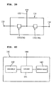
- Fig. 39 shows a duplexer 131 including the piezoelectric resonator according to a preferred embodiment of the present invention.
- This duplexer 131 is provided with an antenna terminal 132, receiving side terminal 133, and a sending side terminal 134.
- This duplexer 131 is configured to include the piezoelectric resonator 135 or piezoelectric filter 136 according to preferred embodiments of the present invention, which permits passage of only high-frequency signals in a required frequency band, between the receiving side terminal 133 and the antenna terminal 132 and between the sending side terminal 134 and the antenna terminal 132.
- Fig. 40 shows a communication apparatus 141.
- This communication apparatus is, for example, a cellular phone.
- This communication apparatus is provided with a receive circuit 142 arranged in a main body, a send circuit 143, and an antenna 144. Signals are transmitted between the antenna 144 and the receive circuit 142 and between the antenna 144 and the send circuit 143 through the duplexer 131 as shown in the fifth preferred embodiment. Consequently, by the piezoelectric resonator or piezoelectric filter according to preferred embodiments of the present invention included in this duplexer 131 as a circuit element, the operating characteristics of this communication apparatus 141 are stabilized and, in addition, selecting and switching of the sending signal and receiving signal are efficiently and effectively performed.
- Fig. 41 shows a modified example of the piezoelectric resonator.
- a concavity 153 extending downward is arranged on the top surface side of a silicon substrate 152 and, in addition, an insulation film 154 made of silicon oxide (SiO 2 ) is arranged to cover the top surface of the silicon substrate 152 and the concavity 153 thereof.
- a lower electrode 155 made of aluminum is arranged with a predetermined pattern on this insulation film 154.
- a piezoelectric thin film 156 made of zinc oxide (ZnO) is arranged on this lower electrode 155 and the insulation film 154.
- a film of an upper electrode 157 made of aluminum is provided on this piezoelectric thin film 156 and overlaps with the lower electrode 155 in the thickness direction.
- the lower electrode 155 and the upper electrode 157 facing each other and a portion of the piezoelectric thin film 156 sandwiched by the two electrodes 155 and 157 constitute a piezoelectric vibration portion 158.
- a portion of the insulation film 154 covering the opening 153 defines a diaphragm 159 supporting this piezoelectric vibration portion 158 such that the piezoelectric vibration portion 158 can vibrate.
- the insulation film 154 is made of silicon oxide (SiO 2 ) as a primary component by an RF magnetron sputtering method. Similar to the method for manufacturing the second preferred embodiment, the gas pressure is within the range of about 0.1 Pa to about 0.25 Pa, and the power density is within the range of about 2.0 (W/cm 2 ) to about 8.5 (W/cm 2 ). Accordingly, the surface roughness of the insulation film 154 is about 0.3 nm on an arithmetic average surface roughness (Ra) basis.
- the stress in this insulation film 154 of the piezoelectric resonator 151 is a compressive stress of about 150 MPa.
- the piezoelectric thin film may be composed of aluminum nitride (AlN) as a primary component.
- the thin film portion sandwiched between the upper electrode and the lower electrode so as to define the vibration portion is composed of at least one layer of piezoelectric thin film, and at least two layers of the piezoelectric thin films may be laminated, or an insulation layer, other than the piezoelectric thin film may be included.
- the piezoelectric resonator may be an element vibrates in a thickness shear vibration mode.
Landscapes
- Chemical & Material Sciences (AREA)
- Physics & Mathematics (AREA)
- Acoustics & Sound (AREA)
- Engineering & Computer Science (AREA)
- Manufacturing & Machinery (AREA)
- Chemical Kinetics & Catalysis (AREA)
- Metallurgy (AREA)
- Organic Chemistry (AREA)
- Crystallography & Structural Chemistry (AREA)
- Mechanical Engineering (AREA)
- Materials Engineering (AREA)
- Signal Processing (AREA)
- Piezo-Electric Or Mechanical Vibrators, Or Delay Or Filter Circuits (AREA)
Applications Claiming Priority (10)
| Application Number | Priority Date | Filing Date | Title |
|---|---|---|---|
| JP2002001329 | 2002-01-08 | ||
| JP2002001329 | 2002-01-08 | ||
| JP2002142350 | 2002-05-17 | ||
| JP2002142350 | 2002-05-17 | ||
| JP2002335120 | 2002-11-19 | ||
| JP2002335120 | 2002-11-19 | ||
| JP2002338036A JP2004221622A (ja) | 2002-01-08 | 2002-11-21 | 圧電共振子、圧電フィルタ、デュプレクサ、通信装置および圧電共振子の製造方法 |
| JP2002338037A JP2004048639A (ja) | 2002-05-17 | 2002-11-21 | 圧電共振子及びその製造方法等 |
| JP2002338037 | 2002-11-21 | ||
| JP2002338036 | 2002-11-21 |
Publications (1)
| Publication Number | Publication Date |
|---|---|
| EP1326332A2 true EP1326332A2 (de) | 2003-07-09 |
Family
ID=27532068
Family Applications (1)
| Application Number | Title | Priority Date | Filing Date |
|---|---|---|---|
| EP03000216A Withdrawn EP1326332A2 (de) | 2002-01-08 | 2003-01-07 | Piezoelektrischer Resonator, piezoelektrisches Filter, Duplexer, Kommunikationsgerät und Herstellungsverfahren des piezoelektrischen Resonators |
Country Status (3)
| Country | Link |
|---|---|
| US (3) | US6906451B2 (de) |
| EP (1) | EP1326332A2 (de) |
| KR (1) | KR100477851B1 (de) |
Cited By (3)
| Publication number | Priority date | Publication date | Assignee | Title |
|---|---|---|---|---|
| WO2004091098A1 (de) * | 2003-04-11 | 2004-10-21 | Epcos Ag | Bauelement mit einer piezoelektrischen funktionsschicht |
| WO2008040325A1 (de) * | 2006-09-29 | 2008-04-10 | Epcos Ag | Mit akustischen volumenwellen arbeitender resonator |
| WO2019095640A1 (zh) * | 2017-11-14 | 2019-05-23 | 安徽云塔电子科技有限公司 | 压电谐振器和压电谐振器的制备方法 |
Families Citing this family (85)
| Publication number | Priority date | Publication date | Assignee | Title |
|---|---|---|---|---|
| FR2842806B1 (fr) * | 2002-07-26 | 2005-07-29 | Mayoly Spindler Lab | Nouveau procede de preparation de derives styryle pyrazoles, isoxazoles et isothiazoles |
| US7275292B2 (en) | 2003-03-07 | 2007-10-02 | Avago Technologies Wireless Ip (Singapore) Pte. Ltd. | Method for fabricating an acoustical resonator on a substrate |
| JP2005073175A (ja) * | 2003-08-27 | 2005-03-17 | Fujitsu Media Device Kk | 圧電薄膜共振子及びその製造方法 |
| JP2005117313A (ja) * | 2003-10-07 | 2005-04-28 | Fujitsu Ltd | 圧電素子およびタッチパネル装置 |
| US7242270B2 (en) * | 2003-10-30 | 2007-07-10 | Avago Technologies Wireless Ip (Singapore) Pte. Ltd. | Decoupled stacked bulk acoustic resonator-based band-pass filter |
| US6946928B2 (en) | 2003-10-30 | 2005-09-20 | Agilent Technologies, Inc. | Thin-film acoustically-coupled transformer |
| US7362198B2 (en) | 2003-10-30 | 2008-04-22 | Avago Technologies Wireless Ip (Singapore) Pte. Ltd | Pass bandwidth control in decoupled stacked bulk acoustic resonator devices |
| US7332985B2 (en) | 2003-10-30 | 2008-02-19 | Avago Technologies Wireless Ip (Singapore) Pte Ltd. | Cavity-less film bulk acoustic resonator (FBAR) devices |
| EP1528677B1 (de) * | 2003-10-30 | 2006-05-10 | Agilent Technologies, Inc. | Akustisch gekoppelter Dünnschicht-Transformator mit zwei piezoelektrischen Elementen, welche entgegengesetzte C-Axen Orientierung besitzten |
| US7019605B2 (en) | 2003-10-30 | 2006-03-28 | Larson Iii John D | Stacked bulk acoustic resonator band-pass filter with controllable pass bandwidth |
| US7615833B2 (en) | 2004-07-13 | 2009-11-10 | Avago Technologies Wireless Ip (Singapore) Pte. Ltd. | Film bulk acoustic resonator package and method of fabricating same |
| US7388454B2 (en) | 2004-10-01 | 2008-06-17 | Avago Technologies Wireless Ip Pte Ltd | Acoustic resonator performance enhancement using alternating frame structure |
| US8981876B2 (en) | 2004-11-15 | 2015-03-17 | Avago Technologies General Ip (Singapore) Pte. Ltd. | Piezoelectric resonator structures and electrical filters having frame elements |
| JP5089860B2 (ja) * | 2004-12-03 | 2012-12-05 | 富士フイルム株式会社 | 圧電アクチュエータ及び液体吐出ヘッド |
| US7202560B2 (en) | 2004-12-15 | 2007-04-10 | Avago Technologies Wireless Ip (Singapore) Pte. Ltd. | Wafer bonding of micro-electro mechanical systems to active circuitry |
| US7791434B2 (en) | 2004-12-22 | 2010-09-07 | Avago Technologies Wireless Ip (Singapore) Pte. Ltd. | Acoustic resonator performance enhancement using selective metal etch and having a trench in the piezoelectric |
| JP4379475B2 (ja) * | 2004-12-24 | 2009-12-09 | 株式会社村田製作所 | 圧電薄膜共振子およびその製造方法 |
| US7427819B2 (en) | 2005-03-04 | 2008-09-23 | Avago Wireless Ip Pte Ltd | Film-bulk acoustic wave resonator with motion plate and method |
| US7369013B2 (en) | 2005-04-06 | 2008-05-06 | Avago Technologies Wireless Ip Pte Ltd | Acoustic resonator performance enhancement using filled recessed region |
| US7436269B2 (en) | 2005-04-18 | 2008-10-14 | Avago Technologies Wireless Ip (Singapore) Pte. Ltd. | Acoustically coupled resonators and method of making the same |
| US7934884B2 (en) * | 2005-04-27 | 2011-05-03 | Lockhart Industries, Inc. | Ring binder cover |
| JP4691395B2 (ja) * | 2005-05-30 | 2011-06-01 | 株式会社日立メディアエレクトロニクス | バルク弾性波共振器、バルク弾性波共振器を用いたフィルタ、それを用いた高周波モジュール、並びにバルク弾性波共振器を用いた発振器 |
| JPWO2007004435A1 (ja) * | 2005-06-30 | 2009-01-22 | パナソニック株式会社 | 音響共振器及びフィルタ |
| US7443269B2 (en) | 2005-07-27 | 2008-10-28 | Avago Technologies General Ip (Singapore) Pte. Ltd. | Method and apparatus for selectively blocking radio frequency (RF) signals in a radio frequency (RF) switching circuit |
| US7868522B2 (en) | 2005-09-09 | 2011-01-11 | Avago Technologies Wireless Ip (Singapore) Pte. Ltd. | Adjusted frequency temperature coefficient resonator |
| US7391286B2 (en) | 2005-10-06 | 2008-06-24 | Avago Wireless Ip Pte Ltd | Impedance matching and parasitic capacitor resonance of FBAR resonators and coupled filters |
| US7423503B2 (en) * | 2005-10-18 | 2008-09-09 | Avago Technologies Wireless Ip (Singapore) Pte. Ltd. | Acoustic galvanic isolator incorporating film acoustically-coupled transformer |
| US7525398B2 (en) | 2005-10-18 | 2009-04-28 | Avago Technologies General Ip (Singapore) Pte. Ltd. | Acoustically communicating data signals across an electrical isolation barrier |
| US7675390B2 (en) | 2005-10-18 | 2010-03-09 | Avago Technologies Wireless Ip (Singapore) Pte. Ltd. | Acoustic galvanic isolator incorporating single decoupled stacked bulk acoustic resonator |
| US7425787B2 (en) | 2005-10-18 | 2008-09-16 | Avago Technologies Wireless Ip (Singapore) Pte. Ltd. | Acoustic galvanic isolator incorporating single insulated decoupled stacked bulk acoustic resonator with acoustically-resonant electrical insulator |
| US7737807B2 (en) | 2005-10-18 | 2010-06-15 | Avago Technologies Wireless Ip (Singapore) Pte. Ltd. | Acoustic galvanic isolator incorporating series-connected decoupled stacked bulk acoustic resonators |
| US7463499B2 (en) | 2005-10-31 | 2008-12-09 | Avago Technologies General Ip (Singapore) Pte Ltd. | AC-DC power converter |
| US7561009B2 (en) | 2005-11-30 | 2009-07-14 | Avago Technologies General Ip (Singapore) Pte. Ltd. | Film bulk acoustic resonator (FBAR) devices with temperature compensation |
| JP2007181185A (ja) * | 2005-12-01 | 2007-07-12 | Sony Corp | 音響共振器およびその製造方法 |
| US7612636B2 (en) | 2006-01-30 | 2009-11-03 | Avago Technologies Wireless Ip (Singapore) Pte. Ltd. | Impedance transforming bulk acoustic wave baluns |
| US7746677B2 (en) | 2006-03-09 | 2010-06-29 | Avago Technologies Wireless Ip (Singapore) Pte. Ltd. | AC-DC converter circuit and power supply |
| US7479685B2 (en) | 2006-03-10 | 2009-01-20 | Avago Technologies General Ip (Singapore) Pte. Ltd. | Electronic device on substrate with cavity and mitigated parasitic leakage path |
| JP2007281031A (ja) * | 2006-04-03 | 2007-10-25 | Seiko Epson Corp | アクチュエータ装置及び液体噴射ヘッド並びに液体噴射装置 |
| US7629865B2 (en) | 2006-05-31 | 2009-12-08 | Avago Technologies Wireless Ip (Singapore) Pte. Ltd. | Piezoelectric resonator structures and electrical filters |
| US7508286B2 (en) | 2006-09-28 | 2009-03-24 | Avago Technologies Wireless Ip (Singapore) Pte. Ltd. | HBAR oscillator and method of manufacture |
| JP2008109402A (ja) * | 2006-10-25 | 2008-05-08 | Toshiba Corp | 薄膜圧電共振器およびその製造方法 |
| WO2008090651A1 (ja) * | 2007-01-24 | 2008-07-31 | Murata Manufacturing Co., Ltd. | 圧電共振子及び圧電フィルタ |
| US8833174B2 (en) * | 2007-04-12 | 2014-09-16 | Colorado School Of Mines | Piezoelectric sensor based smart-die structure for predicting the onset of failure during die casting operations |
| JP4361102B2 (ja) * | 2007-09-12 | 2009-11-11 | 富士フイルム株式会社 | 圧電素子の製造方法 |
| US20090079514A1 (en) * | 2007-09-24 | 2009-03-26 | Tiberiu Jamneala | Hybrid acoustic resonator-based filters |
| US7791435B2 (en) | 2007-09-28 | 2010-09-07 | Avago Technologies Wireless Ip (Singapore) Pte. Ltd. | Single stack coupled resonators having differential output |
| JP5099893B2 (ja) * | 2007-10-22 | 2012-12-19 | 日東電工株式会社 | 透明導電性フィルム、その製造方法及びそれを備えたタッチパネル |
| US7732977B2 (en) | 2008-04-30 | 2010-06-08 | Avago Technologies Wireless Ip (Singapore) | Transceiver circuit for film bulk acoustic resonator (FBAR) transducers |
| US7855618B2 (en) | 2008-04-30 | 2010-12-21 | Avago Technologies Wireless Ip (Singapore) Pte. Ltd. | Bulk acoustic resonator electrical impedance transformers |
| EP2356743A1 (de) | 2008-11-07 | 2011-08-17 | Greenray Industries, Inc. | Kristalloszillator mit verringerter beschleunigungsempfindlichkeit |
| US8248185B2 (en) | 2009-06-24 | 2012-08-21 | Avago Technologies Wireless Ip (Singapore) Pte. Ltd. | Acoustic resonator structure comprising a bridge |
| US8902023B2 (en) | 2009-06-24 | 2014-12-02 | Avago Technologies General Ip (Singapore) Pte. Ltd. | Acoustic resonator structure having an electrode with a cantilevered portion |
| JP5476901B2 (ja) * | 2009-09-30 | 2014-04-23 | ブラザー工業株式会社 | 圧電アクチュエータの製造方法及び圧電アクチュエータ |
| US8193877B2 (en) | 2009-11-30 | 2012-06-05 | Avago Technologies Wireless Ip (Singapore) Pte. Ltd. | Duplexer with negative phase shifting circuit |
| US8796904B2 (en) | 2011-10-31 | 2014-08-05 | Avago Technologies General Ip (Singapore) Pte. Ltd. | Bulk acoustic resonator comprising piezoelectric layer and inverse piezoelectric layer |
| US9243316B2 (en) | 2010-01-22 | 2016-01-26 | Avago Technologies General Ip (Singapore) Pte. Ltd. | Method of fabricating piezoelectric material with selected c-axis orientation |
| US9479139B2 (en) * | 2010-04-29 | 2016-10-25 | Avago Technologies General Ip (Singapore) Pte. Ltd. | Resonator device including electrode with buried temperature compensating layer |
| US9197185B2 (en) | 2010-04-29 | 2015-11-24 | Avago Technologies General Ip (Singapore) Pte. Ltd. | Resonator device including electrodes with buried temperature compensating layers |
| US8830012B2 (en) * | 2010-09-07 | 2014-09-09 | Wei Pang | Composite bulk acoustic wave resonator |
| US8962443B2 (en) | 2011-01-31 | 2015-02-24 | Avago Technologies General Ip (Singapore) Pte. Ltd. | Semiconductor device having an airbridge and method of fabricating the same |
| US9154112B2 (en) | 2011-02-28 | 2015-10-06 | Avago Technologies General Ip (Singapore) Pte. Ltd. | Coupled resonator filter comprising a bridge |
| US9203374B2 (en) | 2011-02-28 | 2015-12-01 | Avago Technologies General Ip (Singapore) Pte. Ltd. | Film bulk acoustic resonator comprising a bridge |
| US9136818B2 (en) | 2011-02-28 | 2015-09-15 | Avago Technologies General Ip (Singapore) Pte. Ltd. | Stacked acoustic resonator comprising a bridge |
| US9425764B2 (en) | 2012-10-25 | 2016-08-23 | Avago Technologies General Ip (Singapore) Pte. Ltd. | Accoustic resonator having composite electrodes with integrated lateral features |
| US9148117B2 (en) | 2011-02-28 | 2015-09-29 | Avago Technologies General Ip (Singapore) Pte. Ltd. | Coupled resonator filter comprising a bridge and frame elements |
| US9083302B2 (en) | 2011-02-28 | 2015-07-14 | Avago Technologies General Ip (Singapore) Pte. Ltd. | Stacked bulk acoustic resonator comprising a bridge and an acoustic reflector along a perimeter of the resonator |
| US9048812B2 (en) | 2011-02-28 | 2015-06-02 | Avago Technologies General Ip (Singapore) Pte. Ltd. | Bulk acoustic wave resonator comprising bridge formed within piezoelectric layer |
| US8575820B2 (en) | 2011-03-29 | 2013-11-05 | Avago Technologies General Ip (Singapore) Pte. Ltd. | Stacked bulk acoustic resonator |
| US9444426B2 (en) | 2012-10-25 | 2016-09-13 | Avago Technologies General Ip (Singapore) Pte. Ltd. | Accoustic resonator having integrated lateral feature and temperature compensation feature |
| US9299914B2 (en) | 2011-04-01 | 2016-03-29 | Renesas Electronics Corporation | Semiconductor device, manufacturing method of the same, and mobile phone |
| US8350445B1 (en) | 2011-06-16 | 2013-01-08 | Avago Technologies Wireless Ip (Singapore) Pte. Ltd. | Bulk acoustic resonator comprising non-piezoelectric layer and bridge |
| KR101776089B1 (ko) * | 2011-07-08 | 2017-09-08 | 삼성전자주식회사 | 표면탄성파 센서 시스템 및 다중울림파를 이용한 측정 방법 |
| JP5905677B2 (ja) * | 2011-08-02 | 2016-04-20 | 太陽誘電株式会社 | 圧電薄膜共振器およびその製造方法 |
| US8922302B2 (en) | 2011-08-24 | 2014-12-30 | Avago Technologies General Ip (Singapore) Pte. Ltd. | Acoustic resonator formed on a pedestal |
| KR101959204B1 (ko) * | 2013-01-09 | 2019-07-04 | 삼성전자주식회사 | 무선 주파수 필터 및 무선 주파수 필터의 제조방법 |
| US9450167B2 (en) | 2013-03-28 | 2016-09-20 | Avago Technologies General Ip (Singapore) Pte. Ltd. | Temperature compensated acoustic resonator device having an interlayer |
| US9608192B2 (en) | 2013-03-28 | 2017-03-28 | Avago Technologies General Ip (Singapore) Pte. Ltd. | Temperature compensated acoustic resonator device |
| US9147826B2 (en) * | 2014-01-23 | 2015-09-29 | Tdk Corporation | Thin film piezoelectric element, thin film piezoelectric actuator, and thin film piezoelectric sensor; and hard disk drive, and inkjet printer |
| US9621126B2 (en) * | 2014-10-22 | 2017-04-11 | Avago Technologies General Ip (Singapore) Pte. Ltd. | Bulk acoustic resonator device including temperature compensation structure comprising low acoustic impedance layer |
| JP2016091589A (ja) * | 2014-11-11 | 2016-05-23 | 株式会社東芝 | サスペンションアッセンブリ、ヘッドサスペンションアッセンブリ、およびこれを備えたディスク装置 |
| US9076469B1 (en) * | 2015-02-11 | 2015-07-07 | Tdk Corporation | Head assembly |
| CN104918201A (zh) * | 2015-04-14 | 2015-09-16 | 歌尔声学股份有限公司 | 一种再加工振膜的方法、振膜以及受话器 |
| JP6724502B2 (ja) * | 2016-04-06 | 2020-07-15 | セイコーエプソン株式会社 | 超音波装置 |
| JP6822118B2 (ja) * | 2016-12-19 | 2021-01-27 | セイコーエプソン株式会社 | 振動子、発振器、電子機器、および移動体 |
| US20180190896A1 (en) * | 2017-01-04 | 2018-07-05 | Te Connectivity Corporation | Ultrasonic Transmitter and Receiver |
Family Cites Families (21)
| Publication number | Priority date | Publication date | Assignee | Title |
|---|---|---|---|---|
| JPS58137317A (ja) | 1982-02-09 | 1983-08-15 | Nec Corp | 圧電薄膜複合振動子 |
| FR2545616B1 (fr) | 1983-05-03 | 1986-10-24 | Commissariat Energie Atomique | Fibres optiques en matiere plastique, notamment multicoeurs, et leur procede de fabrication |
| US4719383A (en) * | 1985-05-20 | 1988-01-12 | The United States Of America As Represented By The United States Department Of Energy | Piezoelectric shear wave resonator and method of making same |
| JPH0346504A (ja) | 1989-07-14 | 1991-02-27 | Murata Mfg Co Ltd | 水晶発振子 |
| JP3107414B2 (ja) | 1991-05-31 | 2000-11-06 | シチズン時計株式会社 | 水晶振動子およびその封止方法 |
| US5504388A (en) * | 1993-03-12 | 1996-04-02 | Ngk Insulators, Ltd. | Piezoelectric/electrostrictive element having electrode film(s) with specified surface roughness |
| US5692279A (en) * | 1995-08-17 | 1997-12-02 | Motorola | Method of making a monolithic thin film resonator lattice filter |
| JP3813740B2 (ja) * | 1997-07-11 | 2006-08-23 | Tdk株式会社 | 電子デバイス用基板 |
| JP3168961B2 (ja) | 1997-10-06 | 2001-05-21 | 住友電気工業株式会社 | ダイヤモンド基板及びダイヤモンド基板の評価方法並びにダイヤモンド表面弾性波フィルタ |
| US6060818A (en) | 1998-06-02 | 2000-05-09 | Hewlett-Packard Company | SBAR structures and method of fabrication of SBAR.FBAR film processing techniques for the manufacturing of SBAR/BAR filters |
| JP3493315B2 (ja) | 1998-12-25 | 2004-02-03 | 京セラ株式会社 | 圧電共振子 |
| JP2000244030A (ja) | 1999-02-23 | 2000-09-08 | Mitsubishi Electric Corp | 圧電体薄膜素子 |
| JP2000278078A (ja) | 1999-03-29 | 2000-10-06 | Kyocera Corp | 圧電共振子 |
| EP1124328A1 (de) | 2000-02-10 | 2001-08-16 | Lucent Technologies Inc. | Herstellungsverfahren eines auf Zinkoxid basierten Resonators |
| US6342134B1 (en) | 2000-02-11 | 2002-01-29 | Agere Systems Guardian Corp. | Method for producing piezoelectric films with rotating magnetron sputtering system |
| US6329305B1 (en) | 2000-02-11 | 2001-12-11 | Agere Systems Guardian Corp. | Method for producing devices having piezoelectric films |
| JP4513169B2 (ja) | 2000-05-17 | 2010-07-28 | 株式会社村田製作所 | 圧電フィルタ、通信装置および圧電フィルタの製造方法 |
| JP3509709B2 (ja) | 2000-07-19 | 2004-03-22 | 株式会社村田製作所 | 圧電薄膜共振子及び圧電薄膜共振子の製造方法 |
| WO2002034096A1 (fr) | 2000-10-27 | 2002-05-02 | Seb S.A. | Boitier de rangement d"accessoires pour un appareil electromenager de preparation culinaire |
| US6515402B2 (en) * | 2001-01-24 | 2003-02-04 | Koninklijke Philips Electronics N.V. | Array of ultrasound transducers |
| JP2004221622A (ja) | 2002-01-08 | 2004-08-05 | Murata Mfg Co Ltd | 圧電共振子、圧電フィルタ、デュプレクサ、通信装置および圧電共振子の製造方法 |
-
2002
- 2002-12-27 US US10/329,602 patent/US6906451B2/en not_active Expired - Lifetime
-
2003
- 2003-01-07 EP EP03000216A patent/EP1326332A2/de not_active Withdrawn
- 2003-01-08 KR KR10-2003-0000982A patent/KR100477851B1/ko not_active Expired - Lifetime
-
2005
- 2005-03-30 US US11/094,622 patent/US7240410B2/en not_active Expired - Lifetime
-
2007
- 2007-05-29 US US11/754,897 patent/US20070221494A1/en not_active Abandoned
Cited By (4)
| Publication number | Priority date | Publication date | Assignee | Title |
|---|---|---|---|---|
| WO2004091098A1 (de) * | 2003-04-11 | 2004-10-21 | Epcos Ag | Bauelement mit einer piezoelektrischen funktionsschicht |
| US7489067B2 (en) | 2003-04-11 | 2009-02-10 | Epcos Ag | Component with a piezoelectric functional layer |
| WO2008040325A1 (de) * | 2006-09-29 | 2008-04-10 | Epcos Ag | Mit akustischen volumenwellen arbeitender resonator |
| WO2019095640A1 (zh) * | 2017-11-14 | 2019-05-23 | 安徽云塔电子科技有限公司 | 压电谐振器和压电谐振器的制备方法 |
Also Published As
| Publication number | Publication date |
|---|---|
| US6906451B2 (en) | 2005-06-14 |
| KR20030060809A (ko) | 2003-07-16 |
| US7240410B2 (en) | 2007-07-10 |
| US20030132683A1 (en) | 2003-07-17 |
| US20050168110A1 (en) | 2005-08-04 |
| US20070221494A1 (en) | 2007-09-27 |
| KR100477851B1 (ko) | 2005-03-22 |
Similar Documents
| Publication | Publication Date | Title |
|---|---|---|
| US7240410B2 (en) | Method for manufacturing a piezoelectric resonator | |
| KR102066960B1 (ko) | 박막 벌크 음향 공진기 및 이를 포함하는 필터 | |
| JP5905677B2 (ja) | 圧電薄膜共振器およびその製造方法 | |
| US7019604B2 (en) | Piezoelectric filter, duplexer, composite piezoelectric resonator, communication device and method for adjusting frequency of piezoelectric filter | |
| JP4624005B2 (ja) | 薄膜バルク音響共鳴器における圧電結合係数を制御して製造される装置 | |
| JP5815329B2 (ja) | 弾性波デバイス | |
| CN115276593B (zh) | 一种声波谐振器及滤波器 | |
| US11018651B2 (en) | Bulk acoustic wave resonators having doped piezoelectric material and an adhesion and diffusion barrier layer | |
| JP2014121025A (ja) | 圧電薄膜共振子 | |
| EP1296451B1 (de) | Oberflächenwellenvorrichtung und Herstellungsverfahren | |
| JP2004221622A (ja) | 圧電共振子、圧電フィルタ、デュプレクサ、通信装置および圧電共振子の製造方法 | |
| JPWO2007119643A1 (ja) | 圧電薄膜共振子、圧電薄膜デバイスおよびその製造方法 | |
| JP2004048639A (ja) | 圧電共振子及びその製造方法等 | |
| KR102691309B1 (ko) | 체적 음향 공진기 | |
| US20050194626A1 (en) | Electronic device and method of fabricating the same | |
| KR102313290B1 (ko) | 박막 벌크 음향 공진기 및 그의 제조 방법 | |
| WO2022135252A1 (zh) | 带温补层的体声波谐振器、滤波器及电子设备 | |
| US7320164B2 (en) | Method of manufacturing an electronic component | |
| JP5848549B2 (ja) | 弾性波デバイスの製造方法 | |
| CN107171653A (zh) | 一种具有高机电耦合系数和高中心频率的声表面波器件 | |
| JP2003060478A (ja) | 圧電薄膜共振子、その製造方法、および、その圧電薄膜共振子を用いたフィルタならびに電子機器 | |
| KR20190008397A (ko) | 박막 벌크 음향 공진기 및 이를 포함하는 필터 | |
| CN117544130A (zh) | 声表面波谐振装置及其形成方法、声表面波滤波装置 | |
| TW202614561A (zh) | Baw諧振器、baw裝置和電子設備 | |
| WO2025205687A1 (ja) | Baw共振器、bawデバイス及び電子機器 |
Legal Events
| Date | Code | Title | Description |
|---|---|---|---|
| PUAI | Public reference made under article 153(3) epc to a published international application that has entered the european phase |
Free format text: ORIGINAL CODE: 0009012 |
|
| 17P | Request for examination filed |
Effective date: 20030107 |
|
| AK | Designated contracting states |
Designated state(s): AT BE BG CH CY CZ DE DK EE ES FI FR GB GR HU IE IT LI LU MC NL PT SE SI SK TR |
|
| AX | Request for extension of the european patent |
Extension state: AL LT LV MK RO |
|
| RAP1 | Party data changed (applicant data changed or rights of an application transferred) |
Owner name: MURATA MANUFACTURING CO., LTD. |
|
| STAA | Information on the status of an ep patent application or granted ep patent |
Free format text: STATUS: THE APPLICATION HAS BEEN WITHDRAWN |
|
| 18W | Application withdrawn |
Effective date: 20070921 |