EP1328048A2 - Dispositif de contrôle d'un élément émetteur de lumière, appareil à transmission optique, méthode et programme d'ordinateur pour déterminer le courant d'alimentation - Google Patents
Dispositif de contrôle d'un élément émetteur de lumière, appareil à transmission optique, méthode et programme d'ordinateur pour déterminer le courant d'alimentation Download PDFInfo
- Publication number
- EP1328048A2 EP1328048A2 EP02028154A EP02028154A EP1328048A2 EP 1328048 A2 EP1328048 A2 EP 1328048A2 EP 02028154 A EP02028154 A EP 02028154A EP 02028154 A EP02028154 A EP 02028154A EP 1328048 A2 EP1328048 A2 EP 1328048A2
- Authority
- EP
- European Patent Office
- Prior art keywords
- current
- optical output
- emitting element
- pulse
- driving
- Prior art date
- Legal status (The legal status is an assumption and is not a legal conclusion. Google has not performed a legal analysis and makes no representation as to the accuracy of the status listed.)
- Granted
Links
- 230000003287 optical effect Effects 0.000 title claims abstract description 225
- 238000000034 method Methods 0.000 title claims description 53
- 238000004590 computer program Methods 0.000 title claims 2
- 239000004065 semiconductor Substances 0.000 claims abstract description 109
- 230000008859 change Effects 0.000 claims description 31
- 230000008033 biological extinction Effects 0.000 claims description 21
- 230000004044 response Effects 0.000 abstract description 6
- 238000006243 chemical reaction Methods 0.000 description 92
- 238000012937 correction Methods 0.000 description 37
- 230000008054 signal transmission Effects 0.000 description 9
- 238000010586 diagram Methods 0.000 description 6
- 230000032683 aging Effects 0.000 description 5
- 230000007613 environmental effect Effects 0.000 description 5
- 238000004891 communication Methods 0.000 description 4
- 238000009795 derivation Methods 0.000 description 4
- 238000012544 monitoring process Methods 0.000 description 4
- 230000008569 process Effects 0.000 description 4
- 238000004364 calculation method Methods 0.000 description 3
- 230000007423 decrease Effects 0.000 description 3
- 230000003247 decreasing effect Effects 0.000 description 3
- 238000001514 detection method Methods 0.000 description 3
- 230000006870 function Effects 0.000 description 3
- 238000005259 measurement Methods 0.000 description 3
- 239000013307 optical fiber Substances 0.000 description 3
- 230000010355 oscillation Effects 0.000 description 2
- 238000012545 processing Methods 0.000 description 2
- 230000008901 benefit Effects 0.000 description 1
- 230000005540 biological transmission Effects 0.000 description 1
- 230000015556 catabolic process Effects 0.000 description 1
- 238000006731 degradation reaction Methods 0.000 description 1
- 239000006185 dispersion Substances 0.000 description 1
- 238000003780 insertion Methods 0.000 description 1
- 230000037431 insertion Effects 0.000 description 1
- 238000007689 inspection Methods 0.000 description 1
- 229920006395 saturated elastomer Polymers 0.000 description 1
- 230000035945 sensitivity Effects 0.000 description 1
- 230000003595 spectral effect Effects 0.000 description 1
Images




Classifications
-
- H—ELECTRICITY
- H01—ELECTRIC ELEMENTS
- H01S—DEVICES USING THE PROCESS OF LIGHT AMPLIFICATION BY STIMULATED EMISSION OF RADIATION [LASER] TO AMPLIFY OR GENERATE LIGHT; DEVICES USING STIMULATED EMISSION OF ELECTROMAGNETIC RADIATION IN WAVE RANGES OTHER THAN OPTICAL
- H01S5/00—Semiconductor lasers
- H01S5/06—Arrangements for controlling the laser output parameters, e.g. by operating on the active medium
- H01S5/068—Stabilisation of laser output parameters
- H01S5/0683—Stabilisation of laser output parameters by monitoring the optical output parameters
- H01S5/06835—Stabilising during pulse modulation or generation
-
- H—ELECTRICITY
- H01—ELECTRIC ELEMENTS
- H01S—DEVICES USING THE PROCESS OF LIGHT AMPLIFICATION BY STIMULATED EMISSION OF RADIATION [LASER] TO AMPLIFY OR GENERATE LIGHT; DEVICES USING STIMULATED EMISSION OF ELECTROMAGNETIC RADIATION IN WAVE RANGES OTHER THAN OPTICAL
- H01S5/00—Semiconductor lasers
- H01S5/06—Arrangements for controlling the laser output parameters, e.g. by operating on the active medium
- H01S5/0617—Arrangements for controlling the laser output parameters, e.g. by operating on the active medium using memorised or pre-programmed laser characteristics
Definitions
- the present invention relates to a light-emitting element controller, an optical transmitting apparatus, and a method and a program for determining a driving current, and more specifically, to a light-emitting element controller which controls a semiconductor light-emitting element, an optical transmitting apparatus, and a method and a program for determining a driving current.
- semiconductor lasers are typically used as light-emitting elements.
- the semiconductor laser has current-optical output characteristics that it emits light when its driving current exceeds a current value called an oscillation threshold current (hereafter, called "threshold current”), and the optical output is proportional to the amount of the driving current exceeding the threshold current.
- threshold current an oscillation threshold current
- the semiconductor laser is driven by a driving current made by superimposing a bias current and a pulse current one upon the other, and drive conditions thereof are appropriately set based on the current-optical output characteristics.
- the current-optical output characteristics vary with its environmental temperature change and aging.
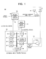
- FIG. 1 is a block diagram showing the configuration of an optical transmitting apparatus according to a first embodiment of the present invention.
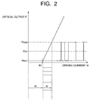
- FIG. 2 is a graph showing an example of current-optical output characteristics of a semiconductor laser.
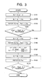
- FIG. 3 is a flowchart showing an example of a control procedure before start of data signal transmission by the optical transmitting apparatus shown in FIG. 1.
- FIG. 4 is a graph showing an example of the current-optical output characteristics of the semiconductor laser controlled based on the procedure shown in FIG. 3.
- FIG. 5 is a flowchart showing an example of a control procedure during the data signal transmission by the optical transmitting apparatus shown in FIG. 1.
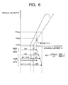
- FIG. 6 is a graph showing an example of the current-optical output characteristics of the current-optical output characteristics of the semiconductor laser controlled based on the procedure shown in FIG. 5.
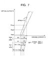
- FIG. 7 is a graph showing another example of the current-optical output characteristics of the semiconductor laser controlled based on the procedure shown in FIG. 5.
- FIG. 8 is a block diagram showing the configuration of an optical transmitting apparatus according to a second embodiment of the present invention.
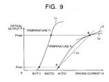
- FIG. 9 is a graph showing temperature dependence of current-optical output characteristics of a semiconductor laser.
- FIG. 10 is a flowchart showing a procedure for deriving a current-light conversion efficiency correction coefficient .(T).
- FIG. 11 is a diagram showing an example of a current-light conversion efficiency correction table.
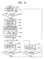
- FIG. 12 is a flowchart showing an example of a control procedure during data signal transmission by the optical transmitting apparatus shown in FIG. 8.
- FIG. 1 is a block diagram showing the configuration of an optical transmitting apparatus 10 according to a first embodiment of the present invention.
- the optical transmitting apparatus (optical transmitter) 10 is a transmitting apparatus which transmits modulated light modulated in correspondence with a data signal, and is constituted of a semiconductor laser 11 being a semiconductor light-emitting element, a monitor PD (Photo Diode) 12, an optical output monitor circuit 13, a bias current drive circuit 14, a pulse current drive circuit 15, and a light-emitting element controller 16.
- the semiconductor laser 11 is a light-emitting element which is driven by a driving current Id made by superimposing a bias current (component) Ib and a pulse current (component) Ip one upon the other.
- the semiconductor laser 11 outputs light (modulated light) which quickly blinks between a plurality of light intensities Pmax and Pmin respectively corresponding to data signals 0 and 1 or the like transmitted by optical communication.
- the monitor PD 12 is a light-receiving element which detects an average optical output (time average of optical output) Pa of the semiconductor laser 11.
- the optical output monitor circuit 13 is a circuit which converts an output from the monitor PD 12 into a voltage signal and outputs it as an output light monitor signal (average optical output information) of the semiconductor laser 11.
- the monitor PD 12 and the optical output monitor circuit 13 do not need to directly detect the modulated light itself (at a plurality of light intensities Pmax and Pmin respectively) from the semiconductor laser 11 but are only required to be able to detect the time average of the modulated light.
- both the monitor PD 12 and the optical output monitor circuit 13 only need to be constituted of detecting means having a low response speed to some degree and do not need to be high-speed detecting means which are often expensive.
- the bias current drive circuit 14 is a circuit which outputs the bias current component Ib of the driving current for driving the semiconductor laser 11, and has a bias control information input unit 17 to which an Ib control signal (bias current control information) is inputted. Based on the bias current control information inputted through the bias control information input unit 17, the bias current component is set which is to be outputted from the bias current drive circuit 14.
- the pulse current drive circuit 15 is a circuit having a pulse control information input unit 18 to which an Ip control signal (pulse current control information) is inputted, and a data signal input unit 19 to which a data signal to be transmitted by optical communication is inputted.
- the pulse current drive circuit 15 outputs the pulse current component corresponding to the data signal inputted to the data signal input unit 19. Further, based on the pulse current control information inputted through the pulse control information input unit 18, the pulse current component is set which is to be outputted from the pulse current drive circuit 15.
- bias current Ib and the pulse current Ip respectively outputted from the bias current drive circuit 14 and the pulse current drive circuit 15 are superimposed one upon the other to be the driving current Id and supplied to the semiconductor laser 11.
- the bias current drive circuit 14 and the pulse current drive circuit 15 are combined to constitute a drive current supply unit which supplies the driving current to the semiconductor laser 11.
- the light-emitting element controller 16 is a control means which inputs thereto the average optical output information from the optical output monitor circuit 13 to generate the Ib control signal and the Ip control signal for controlling a bias current value and a pulse current value, and is constituted of a CPU (Central Processing Unit) 21, a memory (storage device) 30 (a RAM 31, a ROM 32, and a flash memory 33), an A/D converter 41, D/A converters 42 and 43, an I/O (input/output) port 44, and a bus 51.
- a CPU Central Processing Unit
- memory storage device
- A/D converter 41 D/A converters 42 and 43
- I/O (input/output) port 44 an I/O (input/output) port 44
- the CPU 21 which is a processing unit, performs arithmetic and logical operations and conducts a control accompanying execution of a program.
- the memory 30 stores a program and data therein, and is divided into the RAM 31, ROM 32, and flash memory 33.
- the RAM 31 is a volatile memory that has both read and write functions and is used as a work area for storage of data and execution of a program.
- the ROM 32 is a non-volatile memory that normally has only a read function and is used for storage of a program and fixed data.
- the flash memory 33 is an electrically rewritable non-volatile memory and used for storing therein constants for control of the later-described target average optical output, target extinction ratio, and so on, and recording therein a program, so that the program is rewritten from the outside to enable adjustment and change of the control to be performed in correspondence with specifications and variations in characteristics of optical semiconductor lasers and so on.
- the A/D converter 41 is a converter which analog-digital converts an output monitor signal outputted from the optical output monitor circuit 13 and inputs it thereto, and thus serves as an optical output information input unit.
- the D/A converters 42 and 43 are converters respectively which analog-digital convert control information from the CPU 21 and output them as the Ib control signal (bias current control information) and the Ip control signal (pulse current control information) to the bias current drive circuit 14 and the pulse current drive circuit 15, and thus serve as control information output units.
- the I/O port 44 passes data between the CPU 21 and an input/output device outside the optical transmitting apparatus 10. In other words, communication from the outside of the optical transmitting apparatus 10 and control of the semiconductor laser 11 are conducted through the I/O port 44.
- the bus 51 is composed of a plurality of signal lines and passes data among the CPU 21, the memory 30, and so on in the light-emitting element controller 16.
- a microcomputer is used as the light-emitting element controller 16 to control the semiconductor laser 11 using software (program).
- the CPU 21 is operated by the software to constitute a current-optical output coefficient deriving unit which derives a current-optical output coefficient, a pulse current determining unit which determines the pulse current component of the driving current, a bias current determining unit which determines the bias current component of the driving current, and an optical output variation detecting unit which detects a fact that the optical output of the semiconductor light-emitting element falls outside a predetermined tolerance.
- FIG. 2 is a graph showing an example of the current-optical output characteristics of the semiconductor laser 11.
- the semiconductor laser 11 has current-optical output characteristics that it emits light when the driving current Id exceeds an oscillation threshold current Ith (hereafter, threshold current), and an optical output P is proportional to the amount of the driving current exceeding the threshold current.
- a change in the current-optical output characteristics due to variations in temperature environment and so on of the semiconductor laser 11 can be indicated as changes in the threshold current Ith and the current-light conversion efficiency ⁇ .
- the semiconductor laser 11 is driven by the driving current Id made by superimposing the bias current Ib and the pulse current Ip modulated in correspondence with an input data signal one upon the other.
- the bias current Ib is preferably set larger in value than the threshold current Ith. This is for making the time response of the semiconductor laser 11 quicker.
- the optical output P from the semiconductor laser 11 moves between the maximum optical output Pmax and the minimum optical output Pmin in response to ON/OFF of the pulse current Ip.
- the maximum optical output Pmax and the minimum optical output Pmin in this event are represented as in the following equations (2) to (4) using the bias current Ib and the pulse current Ip.
- Pmax ⁇ (Ib + Ip - Ith)
- Pmin ⁇ (Ib - Ith) (Ib ⁇ Ith)
- Pmin 0 (Ib ⁇ Ith)
- the optical output from such an optical transmitting apparatus 10 is often defined by the average optical output Pav and the extinction ratio ER.
- the average optical output Pav and the extinction ratio ER are the same.
- the optical output keeps Pmax during a period during which the data signal indicates data of 1.
- the optical output is at Pmax during the first half of the period during which the data signal indicates data of 1 and the optical output returns to Pmin during the second half thereof.
- the appearance ratio of signals 1 and 0 is often defined as a mark ratio M.
- bias current Ib and the pulse current Ip are represented by the following equations (11) and (12).
- Ip Pav(ER - 1)/[ ⁇ •(1 + a • M • (ER - 1))]
- Ib Pav/[ ⁇ •(1 + a • M • (ER - 1))] + Ith
- the bias current Ib and the pulse current Ip are adjusted using the current-light conversion efficiency ⁇ and the average optical output Pav.
- the threshold current Ith is not directly detected.
- the current-light conversion efficiency ⁇ can be calculated using the same equation (13), irrespective of whether "Ib ⁇ Ith".
- the current-light conversion efficiency ⁇ can be obtained by giving a change of only ⁇ Ip to the pulse current Ip and detecting a change ⁇ Pav in the average optical output Pav at that time.
- the driving current ⁇ Id is set at an amount of change so small as not to affect transmission characteristics, so that the current-light conversion efficiency ⁇ can be detected without stopping output of an optical signal (in the in-service state).
- the current-light conversion efficiency ⁇ is obtained as described below, and further the pulse current Ip is calculated using the equation (11), based on a target average optical output Pav0 and a target extinction ratio ERO. Then, with the pulse current Ip being set to the calculated pulse current Ip, the bias current Ib is adjusted so that the average optical output Pav becomes the target average optical output Pav0. Through such a control, the bias current Ib is automatically adjusted to a value determined from the equation (12).
- the technique eliminates the necessity of the detection of the threshold current Ith and enables adjustment of both the bias current Ib and the pulse current Ip in the in-service state.
- FIG. 3 is a flowchart showing an example of the control procedure before start of the data signal transmission by the optical transmitting apparatus 10, and FIG. 4 is a graph showing the current-optical output characteristics of the semiconductor laser 11 in this event.
- this setting is performed as described below.
- the bias current Ib is gradually increased only by a step pulse current ⁇ Ib (Step S108), the average optical output Pav is referred to (Step S109), and the control is ended at a point of time when the difference between the average optical output Pav and the target average optical output Pav0 becomes equal to or smaller than the tolerance ⁇ (Step S110). It is assumed that the bias current Ib set as described above is Ib01.
- the bias current Ib and the pulse current Ip are set to Ib01 and Ip02 respectively so that the average optical output Pav and the extinction ratio ER become the target values Pav0 and ER0 respectively.
- FIG. 5 is a flowchart showing the control procedure when the current-optical output characteristics of the semiconductor laser 11 change.
- FIGS. 6 and 7 are graphs respectively showing the control procedure and current-optical output characteristics of the semiconductor laser 11 when the average optical output Pav is decreased and increased.
- FIG. 6 shows a case where the bias current Ib becomes smaller than the threshold current Ith.
- FIG. 7 shows a case where the bias current Ib becomes larger than the threshold current Ith with changes in the current-optical output characteristics.
- decreases and increases in the average optical output Pav may be caused by increases and decreases in the threshold current Ith or decreases and increases in the current-light conversion efficiency ⁇ .
- FIG. 8 is a block diagram showing the configuration of an optical transmitting apparatus 20 according to a second embodiment of the present invention.
- the optical transmitting apparatus 20 is a transmitting apparatus which transmits modulated light modulated in correspondence with a data signal, and is constituted of a semiconductor laser 11, a monitor PD 12, an optical output monitor circuit 13, a bias current drive circuit 14, a pulse current drive circuit 15, a light-emitting element controller 60, a thermistor 61, a temperature monitor circuit 62, and an A/D converter 63.
- the optical transmitting apparatus 20 is different from the optical transmitting apparatus 10 in respect of having the thermistor 61, the temperature monitor circuit 62, and the A/D converter 63.
- the thermistor 61 is disposed close to or in contact with the semiconductor laser 11, and changes in resistance in accordance with the temperature of the semiconductor laser 11. In other words, the thermistor 61 serves as a temperature sensor for measuring the temperature of the semiconductor laser 11.
- the temperature monitor circuit 62 is a converter which is electrically connected to the thermistor 61, converts the resistance value of the thermistor 61 into a voltage corresponding to the temperature of the semiconductor laser 11, and outputs it as a temperature monitor signal.
- the A/D converter 63 is a converter which analog-digital converts the temperature monitor signal outputted from the temperature monitor circuit 62 and inputs it thereto, and thus serves as a temperature information input unit.
- a current-light conversion efficiency correction table is stored in a flash memory 33.
- the current-light conversion efficiency correction table is a table showing, in correspondence with a temperature T, a current-light conversion efficiency correction coefficient ⁇ (T) for correcting the error in the current-light conversion efficiency ⁇ caused by nonlinearity of the current-optical output characteristics, and will be explained later in detail.
- a ROM 32 stores software for correcting the current-light conversion efficiency ⁇ using the current-light conversion efficiency correction table.
- This software and a CPU 21 are combined to constitute a current-optical output coefficient correcting unit which corrects the current-light conversion efficiency ⁇ (current-optical output coefficient).
- optical transmitting apparatus 20 is not greatly different from those of the optical transmitting apparatus 10, and thus the description thereof is omitted.
- the current-optical output characteristics of the semiconductor laser 11 are generally linear.
- a possibility is taken into account such that the current-optical output characteristics of the semiconductor laser 11 have nonlinearity.
- the characteristics of the semiconductor laser 11 include nonlinearity to some extent.
- FIG. 9 is a graph showing temperature dependence of the current-optical output characteristics of the semiconductor laser 11.
- graphs L1 and L2 of the current-optical output characteristics are shown in respective cases of a temperature T1 (room temperature) and a temperature T2 (high temperature). Between the minimum optical output Pmin and the maximum optical output Pmax, while the linearity of the current-optical output characteristics is secured at the temperature T1, nonlinearity appears in the current-optical characteristics at the temperature T2.
- the graph L2 does not match a straight line L0 connecting points A and B at the minimum optical output Pmin and the maximum optical output Pmax.
- the minimum optical output Pmin and the maximum optical output Pmax at the temperature T1 are set to secure the linearity of the current-optical output characteristics.
- the maximum optical output Pmax is set beyond a linear region of the current-optical output characteristics, nonlinearity of the current-optical output characteristics may turn into a problem also at the temperature T1.
- a case where nonlinearity appears in the current-optical output characteristics due to a temperature change is described as an example, and the same description also applies to a case where nonlinearity is caused by operating the semiconductor laser 11 at a high optical output.
- the pulse current Ip derived using the equation (11) is larger than the original value. Accordingly, as understood from the equation (9), the extinction ratio ER of the semiconductor laser 11 increases more than necessary. This results in a possibility that the driving current Id corresponding to the minimum optical output Pmin becomes closer to the threshold current Ith of the semiconductor laser 11 or equal to or lower than the threshold current Ith in some cases.
- a line width of emitted light becomes easy to increase.
- the increased line width of emitted light may lead to a possibility that when a pulse of light is transmitted through an optical fiber, the pulse may be deformed (in general, the velocity of light passing through the optical fiber slightly differs depending on the wavelength of the light) to increase dispersion penalty characteristics (degradation in receiver sensitivity when the light from the semiconductor laser 11 is transmitted through the optical fiber).
- the equation (21) corresponds to the equation (13), so that the current-light conversion efficiency ⁇ is measured based on the equation (21).
- the equation (21) is an equation for defining the current-light conversion efficiency ⁇ m(T) being a measurement value.
- the pulse current Ip is changed by a minimal amount ⁇ Ip in this state, the equation (21) is expressed by the following equation (23) (in this event, the bias current Ib is constant, and thus the minimum optical output Pmin does not change), such that where dPmax/dIp is a differential coefficient of a curved line of the current-optical output characteristics (graph L2) at the point of the maximum optical output Pmax (a gradient of a tangent line C of the graph L2 at the point B in FIG. 9).
- the equation (22) is an equation derived on a precondition that the current-optical output characteristics include linearity as in the equation (1).
- the control is a digital control taking only two values at the maximum optical output Pmax and the minimum optical output Pmin. More specifically, it is not necessarily to show the current-optical output characteristics themselves linear as in the equation (1) but it is sufficient to represent only the values at the maximum optical output Pmax and the minimum optical output Pmin by an equation corresponding to the equation (1).
- the equation (25) is shown as a straight line L0 connecting the points A and B at the maximum optical output Pmax and the minimum optical output Pmin of the graph L2 in FIG. 9.
- the Ith0(T) represents the driving current value at a point where this graph intersects the horizontal axis, and a difference between the Ith0(T) and the threshold current Ith(T) of the semiconductor laser 11 itself at the temperature T is tolerated.
- the equation (25) (the straight line L0) always accurately represents the optical output P other than the points A and B (the points at the minimum optical output Pmin and the maximum optical output Pmax).
- the equation (25) accurately represents the relation between the driving current Id and the optical output P.
- the equations (1) to (12) hold even if ⁇ is substituted with ⁇ 0(T), and Ith is substituted with Ith0(T).
- the current-light conversion efficiency correction coefficient ⁇ (T) is obtained in advance, thereby making it possible to appropriately derive the pulse current Ib and so on by substituting the current-light conversion efficiency ⁇ 0(T) measured based on the equation (21) into the equation (27).
- the current-light conversion efficiency correction coefficient ⁇ (T) can be experimentally derived in a manner as described below.
- FIG. 10 is a flowchart showing a procedure for deriving the current-light conversion efficiency correction coefficient ⁇ (T).
- ⁇ (T) a process for deriving the current-light conversion efficiency correction coefficient ⁇ (T) is explained with reference to FIG. 10.
- the semiconductor laser 11 is set to a predetermined temperature T. This setting can be performed by disposing the semiconductor laser 11, for example, in a constant temperature bath and appropriately controlling the constant temperature bath.
- the driving current Id of the semiconductor laser 11 is changed at the temperature T set in Step S501, and the optical output P is measured in this event. This result can be shown, for example, in such a graph in FIG. 9.
- Step S502 From the current-optical output characteristics measured in Step S502, driving currents Id1 and Id2 respectively at the maximum optical output Pmax and the minimum optical output Pmin are obtained.
- the maximum optical output Pmax and the minimum optical value Pmin standard values are often set, and thus those values can be used here.
- the current-light conversion efficiency ⁇ 0(T) can be calculated based on the equation (24) using the minimum optical output Pmin, the maximum optical output Pmax, and the driving currents Id1 and Id2.
- Ip Id2 - Id1.
- the current-light conversion efficiency ⁇ m(T) is represented by the equation (23). Accordingly, the current-light conversion efficiency ⁇ m(T) can be mathematically derived based on the current-optical output characteristics measured in step S502 (the gradient of the tangent line at the point B of the graph L2 in FIG. 9 is obtained).
- the current-light conversion efficiency correction coefficient ⁇ (T) can be derived by dividing ⁇ 0(T) by the current-light conversion efficiency ⁇ m(T) based on the equation (26).
- Steps S502 to S505 are repeated with the temperature setting of the semiconductor laser 11 being changed until the current-light conversion efficiency correction coefficients ⁇ (T) at all set temperatures, are derived.
- FIG. 11 is a diagram showing an example of a current-light conversion efficiency correction table including the current-light conversion efficiency correction coefficients ⁇ (T).
- the current-light conversion efficiency correction coefficients ⁇ (T) are shown in correspondence with temperatures T.
- the current-light conversion efficiency correction coefficients ⁇ (T) are 1.0 from a low temperature (-40°C) to room temperature (25°C).
- the current-light conversion efficiencies ⁇ m and ⁇ 0 are almost the same, so that the nonlinearity of the current-optical output characteristics can be almost neglected between the minimum optical output Pmin and the maximum optical output Pmax.
- the current-light conversion efficiency correction coefficients ⁇ (T) are larger than 1 at high temperatures (75°C to 85°C) at which nonlinearity occurs in the current-optical output characteristics between the maximum optical output Pmax and the minimum optical output Pmin.
- FIG. 12 is a flowchart showing a control procedure when the current-optical output characteristics of the semiconductor laser 11 including the nonlinearity change.
- Steps S601 to S603 are inserted in place of Step S205 in FIG. 5.
- the current-light conversion efficiency correction coefficients ⁇ (T) are used on a precondition that the current-light conversion efficiencies ⁇ m correspond to the gradient of the current-optical output (the gradient of the straight line C in FIG. 9) at the point of the maximum optical output Pmax (refer to the equations (23) and (27)).
- the average optical output Pav during the in-service state is monitored at all times in Steps S201 and S202 and thus never greatly deviates from the reference value Pav1, so that the semiconductor laser 11 is digitally operated near the target values of the minimum optical output Pmin and the maximum optical output Pmax. This makes it possible to appropriately correct the current-light conversion efficiencies ⁇ m using the current-light conversion efficiency correction coefficients ⁇ (T) based on the equations (23) and (27).
- Steps S206 to S213 are the same processes as those explained in the first embodiment, and thus the description thereof is omitted.
- the bias current Ib and the pulse current Ip are set so that the average optical output Pav and the extinction ratio ER become the target values Pav0 and ER0 respectively. Note that this also means that the minimum optical output Pmin and the maximum optical output Pmax are set at the target values.
- Steps S210 and S213 When the setting is completed in Steps S210 and S213, the procedure returns to Step 201, and monitoring is performed whether the average optical output Pav matches the target average optical output Pav0.
- the current-light conversion efficiency ⁇ can be corrected before start of the service also in this embodiment.
- the flowchart for enabling the above correction is shown by inserting the processes of Steps S601 to S603 in FIG. 12 in place of Step S107 in FIG. 3. This flowchart is not greatly different from that in FIG. 12 in the point of correction of the current-light conversion efficiency ⁇ , and thus the detailed description thereof is omitted.
- the embodiment of the present invention is not limited to the above-described embodiment, but can be extended and modified. Extended and modified embodiments are also included in the technical scope of the present invention.
Landscapes
- Physics & Mathematics (AREA)
- Condensed Matter Physics & Semiconductors (AREA)
- General Physics & Mathematics (AREA)
- Electromagnetism (AREA)
- Optics & Photonics (AREA)
- Semiconductor Lasers (AREA)
Applications Claiming Priority (4)
| Application Number | Priority Date | Filing Date | Title |
|---|---|---|---|
| JP2001388006 | 2001-12-20 | ||
| JP2001388006 | 2001-12-20 | ||
| JP2002357930 | 2002-12-10 | ||
| JP2002357930A JP3748432B2 (ja) | 2001-12-20 | 2002-12-10 | 発光素子制御装置、光送信装置、駆動電流決定方法、およびプログラム |
Publications (3)
| Publication Number | Publication Date |
|---|---|
| EP1328048A2 true EP1328048A2 (fr) | 2003-07-16 |
| EP1328048A3 EP1328048A3 (fr) | 2005-07-13 |
| EP1328048B1 EP1328048B1 (fr) | 2006-10-18 |
Family
ID=26625187
Family Applications (1)
| Application Number | Title | Priority Date | Filing Date |
|---|---|---|---|
| EP02028154A Expired - Lifetime EP1328048B1 (fr) | 2001-12-20 | 2002-12-19 | Dispositif de contrôle d'un élément émetteur de lumière, appareil à transmission optique, méthode et programme d'ordinateur pour déterminer le courant d'alimentation |
Country Status (4)
| Country | Link |
|---|---|
| US (1) | US6895028B2 (fr) |
| EP (1) | EP1328048B1 (fr) |
| JP (1) | JP3748432B2 (fr) |
| DE (1) | DE60215452T2 (fr) |
Cited By (1)
| Publication number | Priority date | Publication date | Assignee | Title |
|---|---|---|---|---|
| GB2432037B (en) * | 2005-11-01 | 2011-04-20 | Agilent Technologies Inc | A method and system for stabilizing operation of laser sources |
Families Citing this family (16)
| Publication number | Priority date | Publication date | Assignee | Title |
|---|---|---|---|---|
| EP1536577A1 (fr) * | 2002-07-19 | 2005-06-01 | Matsushita Electric Industrial Co., Ltd. | Circuit de commande du rapport d'extinction d'un signal en rafale, circuit integre correspondant, procede de commande du rapport d'extinction d'un signal en rafale, programme informatique, et circuit d'attaque a diode laser |
| JPWO2004074805A1 (ja) * | 2003-02-18 | 2006-06-01 | 富士通株式会社 | 光源装置 |
| EP1594238A3 (fr) * | 2004-05-06 | 2006-05-03 | Avanex Corporation | Procédé et système de commande de diodes laser dans des systèmes de communications optiques |
| US20060126684A1 (en) * | 2004-12-10 | 2006-06-15 | Chien-Chang Liu | Real time constant excitation ratio (ER) laser driving circuit |
| CN101120408A (zh) * | 2005-01-10 | 2008-02-06 | 皇家飞利浦电子股份有限公司 | 防止激光二极管饱和的方法和装置 |
| JP2006210812A (ja) * | 2005-01-31 | 2006-08-10 | Sumitomo Electric Ind Ltd | 光出力制御回路及び光出力制御方法 |
| US20070116076A1 (en) * | 2005-11-21 | 2007-05-24 | Frank Wang | Controlling optical power and extincation ratio of a semiconductor laser |
| JP5233235B2 (ja) * | 2007-10-10 | 2013-07-10 | セイコーエプソン株式会社 | 半導体発光素子の制御 |
| US8350495B2 (en) | 2009-06-05 | 2013-01-08 | Light-Based Technologies Incorporated | Device driver providing compensation for aging |
| JP4885289B2 (ja) * | 2010-04-21 | 2012-02-29 | 古河電気工業株式会社 | 面発光レーザ装置 |
| JP2012142417A (ja) * | 2010-12-28 | 2012-07-26 | Sumitomo Electric Device Innovations Inc | レーザダイオードの制御方法 |
| JP2012160392A (ja) * | 2011-02-02 | 2012-08-23 | Stanley Electric Co Ltd | 点灯制御装置 |
| WO2015087448A1 (fr) * | 2013-12-13 | 2015-06-18 | 富士通株式会社 | Systeme de transmission par fibres optiques multiporteuses, procede de transmission par fibres optiques multiporteuses, emetteur optique et recepteur optique |
| JP6771810B2 (ja) * | 2015-04-20 | 2020-10-21 | 住友重機械工業株式会社 | レーザ加工装置 |
| JP6717082B2 (ja) * | 2016-06-30 | 2020-07-01 | 富士通オプティカルコンポーネンツ株式会社 | 光送信モジュールおよび光送信モジュールの制御方法 |
| DE102021207593A1 (de) | 2021-07-16 | 2023-01-19 | Robert Bosch Gesellschaft mit beschränkter Haftung | Vorrichtung und Verfahren zum Betreiben eines Treibers zum Ansteuern mindestens einer angeschlossenen Laserdiode auf Basis einer Abfolge von Lichtintensitäts-Eingangswerten |
Family Cites Families (18)
| Publication number | Priority date | Publication date | Assignee | Title |
|---|---|---|---|---|
| JP2747311B2 (ja) * | 1989-02-06 | 1998-05-06 | 日本ディジタルイクイップメント株式会社 | デジタル光通信装置に使用される光送信装置のイネーブル応答時間を制御する装置および方法 |
| US4998257A (en) * | 1989-03-09 | 1991-03-05 | Konica Corporation | Semiconductor laser driving apparatus |
| JP3024398B2 (ja) * | 1992-11-12 | 2000-03-21 | 日本電気株式会社 | Ld駆動回路 |
| DE4316811A1 (de) * | 1993-05-19 | 1994-11-24 | Philips Patentverwaltung | Optisches Übertragungssystem mit einer Laserdiode |
| JPH07135486A (ja) * | 1993-11-10 | 1995-05-23 | Fujitsu Ltd | 光送信回路の自動パワー制御方法及び光送信回路の自動パワー制御回路 |
| JP3541407B2 (ja) | 1993-11-25 | 2004-07-14 | 松下電器産業株式会社 | 光ファイバーモジュールのld駆動回路 |
| JPH088831A (ja) * | 1994-06-22 | 1996-01-12 | Fujitsu Ltd | 光送信機 |
| US5579328A (en) * | 1995-08-10 | 1996-11-26 | Northern Telecom Limited | Digital control of laser diode power levels |
| JP2856247B2 (ja) * | 1996-11-12 | 1999-02-10 | 日本電気株式会社 | 消光比劣化を防止するapc方式 |
| JP2877209B2 (ja) | 1996-12-04 | 1999-03-31 | 日本電気株式会社 | 光出力レベル制御方法及び光出力レベル制御装置 |
| JP3636411B2 (ja) * | 1997-03-19 | 2005-04-06 | 富士通株式会社 | レーザーダイオードの駆動回路および駆動方法 |
| JPH11135871A (ja) * | 1997-10-28 | 1999-05-21 | Nec Corp | レーザダイオード駆動方法および回路 |
| JP3085274B2 (ja) * | 1998-01-19 | 2000-09-04 | 日本電気株式会社 | 光送信器 |
| US6055252A (en) * | 1998-09-10 | 2000-04-25 | Photonic Solutions, Inc. | Fiberoptic transmitter using thermistor to maintain stable operating conditions over a range of temperature |
| JP4107532B2 (ja) * | 1999-01-12 | 2008-06-25 | ミヤチテクノス株式会社 | レーザ装置 |
| US6707833B1 (en) * | 2000-03-31 | 2004-03-16 | Marconi Communications, Inc. | Digital laser driver circuit |
| JP3637872B2 (ja) * | 2001-02-08 | 2005-04-13 | 日本電気株式会社 | フィードフォワード型apc回路を備えたレーザダイオード駆動回路および方法 |
| US6661817B1 (en) * | 2001-09-18 | 2003-12-09 | International Business Machines Corporation | Laser diode monitoring via current mirroring |
-
2002
- 2002-12-10 JP JP2002357930A patent/JP3748432B2/ja not_active Expired - Fee Related
- 2002-12-12 US US10/317,799 patent/US6895028B2/en not_active Expired - Fee Related
- 2002-12-19 EP EP02028154A patent/EP1328048B1/fr not_active Expired - Lifetime
- 2002-12-19 DE DE60215452T patent/DE60215452T2/de not_active Expired - Lifetime
Cited By (1)
| Publication number | Priority date | Publication date | Assignee | Title |
|---|---|---|---|---|
| GB2432037B (en) * | 2005-11-01 | 2011-04-20 | Agilent Technologies Inc | A method and system for stabilizing operation of laser sources |
Also Published As
| Publication number | Publication date |
|---|---|
| EP1328048B1 (fr) | 2006-10-18 |
| DE60215452D1 (de) | 2006-11-30 |
| US6895028B2 (en) | 2005-05-17 |
| US20030118063A1 (en) | 2003-06-26 |
| EP1328048A3 (fr) | 2005-07-13 |
| JP2003249716A (ja) | 2003-09-05 |
| JP3748432B2 (ja) | 2006-02-22 |
| DE60215452T2 (de) | 2007-08-23 |
Similar Documents
| Publication | Publication Date | Title |
|---|---|---|
| EP1328048A2 (fr) | Dispositif de contrôle d'un élément émetteur de lumière, appareil à transmission optique, méthode et programme d'ordinateur pour déterminer le courant d'alimentation | |
| US7443897B2 (en) | Method for distinguish failure modes in an APC circuit and an optical transmitter using the same | |
| US8275011B2 (en) | Optical transmission module, wavelength monitor, and wavelength drift detection method | |
| US20050249252A1 (en) | Method and apparatus for digital signal processing enhanced laser performance compensation | |
| US20030165168A1 (en) | Laser diode control circuit and laser diode control method | |
| US7483455B2 (en) | Control method and control circuit for laser diode, and optical transmitter using the same | |
| US7940822B1 (en) | Tracking injection seeding power based on back facet monitoring (BFM) of an injection seeded laser | |
| EP1233488A1 (fr) | Source de lumière | |
| US20040246460A1 (en) | Method and device for adjusting a laser | |
| US7653102B2 (en) | Method and apparatus for controlling output power levels of a laser used for optical data transmission based on data rate-speed optical feedback | |
| US5926495A (en) | Laser diode pump wavelength sensing and control apparatus and method | |
| US7738796B2 (en) | Method and apparatus for digital signal processing enhanced laser performance compensation | |
| US20050201430A1 (en) | Laser oscillator | |
| EP1167943A2 (fr) | Détecter le vieillissement des composantes optiques | |
| JP2929992B2 (ja) | 光送信回路 | |
| JP2005085815A (ja) | 波長安定化装置 | |
| KR102574422B1 (ko) | 광 송신 장치의 컨트롤러 | |
| US7787507B2 (en) | Method and apparatus for controlling laser modulation based on measurements of average laser output power | |
| JP2013016689A (ja) | レーザ溶接電源のレーザ出力校正方法および校正装置 | |
| JPH07221369A (ja) | 回路素子の劣化検出回路 | |
| JP2008084963A (ja) | レーザダイオード駆動回路 | |
| US20200033243A1 (en) | Method of Estimating a Condition Parameter of a Laser Diode with an Associated Photodiode, Apparatus for Monitoring the Operation of Such Laser Diode and Particular Sensor Apparatus | |
| JP2009049031A (ja) | レーザダイオード制御回路 | |
| JP2830794B2 (ja) | 光送信回路 | |
| JPH11251674A (ja) | 光送信器、及び光送信器における光出力及び波長の制御方法 |
Legal Events
| Date | Code | Title | Description |
|---|---|---|---|
| PUAI | Public reference made under article 153(3) epc to a published international application that has entered the european phase |
Free format text: ORIGINAL CODE: 0009012 |
|
| 17P | Request for examination filed |
Effective date: 20021219 |
|
| AK | Designated contracting states |
Designated state(s): AT BE BG CH CY CZ DE DK EE ES FI FR GB GR IE IT LI LU MC NL PT SE SI SK TR |
|
| AX | Request for extension of the european patent |
Extension state: AL LT LV MK RO |
|
| PUAL | Search report despatched |
Free format text: ORIGINAL CODE: 0009013 |
|
| AK | Designated contracting states |
Kind code of ref document: A3 Designated state(s): AT BE BG CH CY CZ DE DK EE ES FI FR GB GR IE IT LI LU MC NL PT SE SI SK TR |
|
| AX | Request for extension of the european patent |
Extension state: AL LT LV MK RO |
|
| AKX | Designation fees paid |
Designated state(s): DE FR GB |
|
| GRAP | Despatch of communication of intention to grant a patent |
Free format text: ORIGINAL CODE: EPIDOSNIGR1 |
|
| GRAS | Grant fee paid |
Free format text: ORIGINAL CODE: EPIDOSNIGR3 |
|
| GRAA | (expected) grant |
Free format text: ORIGINAL CODE: 0009210 |
|
| AK | Designated contracting states |
Kind code of ref document: B1 Designated state(s): DE FR GB |
|
| REG | Reference to a national code |
Ref country code: GB Ref legal event code: FG4D |
|
| REF | Corresponds to: |
Ref document number: 60215452 Country of ref document: DE Date of ref document: 20061130 Kind code of ref document: P |
|
| ET | Fr: translation filed | ||
| PLBE | No opposition filed within time limit |
Free format text: ORIGINAL CODE: 0009261 |
|
| STAA | Information on the status of an ep patent application or granted ep patent |
Free format text: STATUS: NO OPPOSITION FILED WITHIN TIME LIMIT |
|
| 26N | No opposition filed |
Effective date: 20070719 |
|
| GBPC | Gb: european patent ceased through non-payment of renewal fee |
Effective date: 20070118 |
|
| PG25 | Lapsed in a contracting state [announced via postgrant information from national office to epo] |
Ref country code: GB Free format text: LAPSE BECAUSE OF NON-PAYMENT OF DUE FEES Effective date: 20070118 |
|
| PGFP | Annual fee paid to national office [announced via postgrant information from national office to epo] |
Ref country code: DE Payment date: 20101215 Year of fee payment: 9 |
|
| PGFP | Annual fee paid to national office [announced via postgrant information from national office to epo] |
Ref country code: FR Payment date: 20111219 Year of fee payment: 10 |
|
| REG | Reference to a national code |
Ref country code: FR Ref legal event code: ST Effective date: 20130830 |
|
| REG | Reference to a national code |
Ref country code: DE Ref legal event code: R119 Ref document number: 60215452 Country of ref document: DE Effective date: 20130702 |
|
| PG25 | Lapsed in a contracting state [announced via postgrant information from national office to epo] |
Ref country code: DE Free format text: LAPSE BECAUSE OF NON-PAYMENT OF DUE FEES Effective date: 20130702 |
|
| PG25 | Lapsed in a contracting state [announced via postgrant information from national office to epo] |
Ref country code: FR Free format text: LAPSE BECAUSE OF NON-PAYMENT OF DUE FEES Effective date: 20130102 |