EP1333662A2 - CMOS Bildsensor - Google Patents
CMOS Bildsensor Download PDFInfo
- Publication number
- EP1333662A2 EP1333662A2 EP02258331A EP02258331A EP1333662A2 EP 1333662 A2 EP1333662 A2 EP 1333662A2 EP 02258331 A EP02258331 A EP 02258331A EP 02258331 A EP02258331 A EP 02258331A EP 1333662 A2 EP1333662 A2 EP 1333662A2
- Authority
- EP
- European Patent Office
- Prior art keywords
- wirings
- fixed potential
- image sensor
- circuits
- cmos image
- Prior art date
- Legal status (The legal status is an assumption and is not a legal conclusion. Google has not performed a legal analysis and makes no representation as to the accuracy of the status listed.)
- Withdrawn
Links
Images





Classifications
-
- H—ELECTRICITY
- H04—ELECTRIC COMMUNICATION TECHNIQUE
- H04N—PICTORIAL COMMUNICATION, e.g. TELEVISION
- H04N25/00—Circuitry of solid-state image sensors [SSIS]; Control thereof
- H04N25/60—Noise processing, e.g. detecting, correcting, reducing or removing noise
- H04N25/616—Noise processing, e.g. detecting, correcting, reducing or removing noise involving a correlated sampling function, e.g. correlated double sampling [CDS] or triple sampling
-
- H—ELECTRICITY
- H04—ELECTRIC COMMUNICATION TECHNIQUE
- H04N—PICTORIAL COMMUNICATION, e.g. TELEVISION
- H04N25/00—Circuitry of solid-state image sensors [SSIS]; Control thereof
- H04N25/60—Noise processing, e.g. detecting, correcting, reducing or removing noise
- H04N25/65—Noise processing, e.g. detecting, correcting, reducing or removing noise applied to reset noise, e.g. KTC noise related to CMOS structures by techniques other than CDS
-
- H—ELECTRICITY
- H04—ELECTRIC COMMUNICATION TECHNIQUE
- H04N—PICTORIAL COMMUNICATION, e.g. TELEVISION
- H04N25/00—Circuitry of solid-state image sensors [SSIS]; Control thereof
- H04N25/70—SSIS architectures; Circuits associated therewith
- H04N25/76—Addressed sensors, e.g. MOS or CMOS sensors
-
- H—ELECTRICITY
- H10—SEMICONDUCTOR DEVICES; ELECTRIC SOLID-STATE DEVICES NOT OTHERWISE PROVIDED FOR
- H10F—INORGANIC SEMICONDUCTOR DEVICES SENSITIVE TO INFRARED RADIATION, LIGHT, ELECTROMAGNETIC RADIATION OF SHORTER WAVELENGTH OR CORPUSCULAR RADIATION
- H10F39/00—Integrated devices, or assemblies of multiple devices, comprising at least one element covered by group H10F30/00, e.g. radiation detectors comprising photodiode arrays
- H10F39/10—Integrated devices
- H10F39/12—Image sensors
- H10F39/18—Complementary metal-oxide-semiconductor [CMOS] image sensors; Photodiode array image sensors
-
- H—ELECTRICITY
- H10—SEMICONDUCTOR DEVICES; ELECTRIC SOLID-STATE DEVICES NOT OTHERWISE PROVIDED FOR
- H10F—INORGANIC SEMICONDUCTOR DEVICES SENSITIVE TO INFRARED RADIATION, LIGHT, ELECTROMAGNETIC RADIATION OF SHORTER WAVELENGTH OR CORPUSCULAR RADIATION
- H10F39/00—Integrated devices, or assemblies of multiple devices, comprising at least one element covered by group H10F30/00, e.g. radiation detectors comprising photodiode arrays
- H10F39/80—Constructional details of image sensors
- H10F39/802—Geometry or disposition of elements in pixels, e.g. address-lines or gate electrodes
-
- H—ELECTRICITY
- H10—SEMICONDUCTOR DEVICES; ELECTRIC SOLID-STATE DEVICES NOT OTHERWISE PROVIDED FOR
- H10F—INORGANIC SEMICONDUCTOR DEVICES SENSITIVE TO INFRARED RADIATION, LIGHT, ELECTROMAGNETIC RADIATION OF SHORTER WAVELENGTH OR CORPUSCULAR RADIATION
- H10F39/00—Integrated devices, or assemblies of multiple devices, comprising at least one element covered by group H10F30/00, e.g. radiation detectors comprising photodiode arrays
- H10F39/80—Constructional details of image sensors
- H10F39/803—Pixels having integrated switching, control, storage or amplification elements
Definitions
- This invention relates to a CMOS image sensor for getting images by outputting in order image signals sensed in each of pixel areas arranged like a matrix on the basis of X-Y addressing.
- CCDs charge coupled devices
- CMOS image sensors which can be produced by the process for producing complementary metal-oxide semiconductors (CMOSes), which can operate at a low voltage, which consume only a small amount of power, and the unit cost of the production of which is low.
- CMOS image sensors In CMOS image sensors, pixel circuits each of which gets an image corresponding to one pixel are arranged like a matrix. They output image signals corresponding to an entire image by selecting in order output from each pixel circuit with a vertical scanning shift register and horizontal scanning shift register.
- Fig. 7 is a view showing the structure of a pixel circuit in a previously-considered CMOS image sensor.
- a pixel circuit 70 shown in Fig. 7 includes a photodiode D71 as a photoelectric conversion element and has an active pixel sensor (APS) structure in which a reset transistor M71, source follower amplifier M72, and row selection transistor M73 each formed by, for example, an n-channel MOS field-effect transistor (MOSFET) are located.
- APS active pixel sensor
- the anode side of the photodiode D71 is grounded and the cathode side is connected to a source electrode on the reset transistor M71 and a gate electrode on the source follower amplifier M72.
- a drain electrode on the reset transistor M71 and a drain electrode on the source follower amplifier M72 are connected to a power supply line L71 where reset voltage VR is supplied.
- a gate electrode on the reset transistor M71 is connected to a reset signal line L72 where a reset signal RST is supplied.
- a source electrode on the source follower amplifier M72 is connected to a drain electrode on the row selection transistor M73.
- a gate electrode on the row selection transistor M73 is connected to a row selection signal line L73 where a row selection signal SLCT for selecting the pixel circuit 70 in a row direction is supplied.
- a source electrode on the row selection transistor M73 is connected to a column selection signal line L74 for selecting the pixel circuit 70 in a column direction.
- the photodiode D71 is charged by reset voltage VR when the reset transistor M71 goes into the ON state with predetermined timing due to a reset signal RST.
- the photodiode D71 begins to discharge and its potential drops from the reset voltage VR.
- a row selection signal SLCT is input to the gate electrode on the row selection transistor M73.
- the voltage of the source of the source follower amplifier M72 is gotten as a signal voltage via the column selection signal line L74.
- the column selection signal line L74 is connected to, for example, a drain electrode on a column selection transistor (not shown) via an amplifier/noise cancel circuit (not shown).
- each of the pixel circuits 70 arranged in a horizontal direction is selected by a row selection signal SLCT, the column selection transistors each connected to the column selection signal line L74 are put in order into the ON state, and image signals corresponding to one pixel are output in order.
- CMOS image sensors having the above APS structure
- reset noise produced at the source electrode on the reset transistor M71 at the time of a reset signal RST being put into the OFF state will degrade output image signals.
- the pixel circuits 70 differ from one another in this reset noise due to, for example, variation in threshold voltage VT for the reset transistors M71.
- correlated double sampling (CDS) circuits have been used to reduce this reset noise.
- a CDS circuit is located in each column in the amplifier/noise cancel circuit connected to each column selection signal line L74.
- the relation between the operation of this CDS circuit and each pixel circuit 70 is as follows. A signal voltage output from the pixel circuit 70 is sampled first by the CDS circuit. Then the photodiode D71 in the pixel circuit 70 is reset to reset voltage VR and voltage output from the pixel circuit 70 at the time of a reset is sampled by the CDS circuit. And then the difference between the voltage output at the time of a reset and signal voltage is calculated. This cancels out reset noise and only image signals can be extracted.
- a CDS circuit for reducing reset noise is located in each column.
- Fig. 8 is a view for intelligibly describing how to locate CDS circuits in circuits in a conventional CMOS image sensor.
- CDS circuits 80 are arranged in a horizontal direction in the same way as the column selection signal lines L74 located parallel to one another by n columns in a horizontal direction.
- the input side of each CDS circuit 80 is connected to an output section of each pixel circuit 70 via each column selection signal line L74 and the output side is connected to, for example, a drain electrode on each column selection transistor (not shown).
- each CDS circuit 80 has the same wiring pattern. Therefore, if the CDS circuits 80 are located parallel to one another in this way, a portion of a signal transmission wiring for transmitting a signal output from the pixel circuit 70 which is located parallel to a signal transmission wiring in an adjacent CDS circuit 80 increases. Therefore, if a high integration level leads to a narrow space between the CDS circuits 80, image signals from pixels adjacent to each other in a horizontal direction will interfere due to parasitic capacitance between the signal transmission wirings. For example, if there are an area with strong brightness and an area with dim brightness on an image gotten, the border between these areas may not be displayed distinctly.
- interference between adjacent image signals has been controlled by increasing the capacitance of a capacitive element for sampling included in the CDS circuit 80.
- the interference has been controlled by increasing operating current for an amplifier located in the CDS circuit 80.
- CMOS image sensor being able to get distinct images in which interference does not occur between adjacent pixels without changing an element in a circuit.
- CMOS image sensor for getting images by outputting in order image signals sensed in each of pixel areas arranged like a matrix on the basis of X-Y addressing.
- This CMOS image sensor comprises a plurality of pixel circuits arranged like a matrix and each including a photoelectric conversion element to make the photoelectric conversion of incident light for outputting the image signals corresponding to one pixel, a plurality of signal processing circuits arranged by the number equal to that of the pixel circuits arranged in a horizontal direction and connected to all the pixel circuits arranged in a vertical direction for performing predetermined signal processing on the image signals from each of all the pixel circuits arranged in the vertical direction, a horizontal scanning circuit for switching and outputting in order the image signals from the plurality of signal processing circuits, and fixed potential wirings parallel to one another and each located between two of the plurality of signal processing circuits arranged.
- Fig. 1 is a view for describing the principles underlying an embodiment of the present invention. An overview of an embodiment of the present invention will be given by using Fig. 1.
- a CMOS image sensor 1 shown in Fig. 1 comprises a pixel section 2 where pixel circuits 2a are arranged like a matrix, a vertical scanning circuit 3 for selecting output from a row of pixel circuits 2a, signal processing circuits 4 for performing predetermined signal processing on image signals output from pixel circuits 2a in each column, and a horizontal scanning circuit 5 for switching and outputting image signals from each signal processing circuit 4.
- Each of fixed potential wirings 6 having constant potential is located between the signal processing circuits 4.
- the pixel circuits 2a are arranged in four rows and four columns in the pixel section 2 in Fig. 1, but in reality more pixel circuits 2a will be arranged there.
- one row selection signal line 3a is connected to each horizontal row of pixel circuits 2a and one column selection signal line 5a is connected to each vertical column of pixel circuits 2a.
- Each pixel circuit 2a includes a photoelectric conversion element for making the photoelectric conversion of incident light and outputs image signals corresponding to one pixel to the column selection signal line 5a connected thereto.
- the vertical scanning circuit 3 selects output from a row of pixel circuits 2a by outputting a row selection signal to any row selection signal line 3a.
- Image signals output to the column selection signal line 5a are input to the horizontal scanning circuit 5 via the signal processing circuit 4 in each column.
- the horizontal scanning circuit 5 selects and outputs image signals from each column in order.
- All the signal processing circuits 4 on the column selection signal lines 5a have the same circuit structure, perform predetermined signal processing on input image signals, and output them to the horizontal scanning circuit 5.
- amplifier circuits, noise cancel circuits, or the like are located as the signal processing circuits 4.
- CDS circuits are located as these noise cancel circuits.
- the column selection signal lines 5a in the columns located from the pixel section 2 to the horizontal scanning circuit 5 are parallel to one another.
- the signal processing circuits 4 located in the columns are also parallel to one another.
- the signal processing circuits 4 include signal transmission wirings for transmitting image signals. These signal transmission wirings always include one or more signal transmission wirings for transmitting image signals in a column direction.
- the integration level of the pixel circuits 2a is high and space between adjacent signal processing circuits 4 is very narrow. Therefore, image signals transmitted in different columns will interfere due to wiring capacitance between signal transmission wirings located in a column direction in adjacent signal processing circuits 4.
- the fixed potential wirings 6 having constant potential are located parallel to one another.
- Each fixed potential wiring 6 is located between adjacent signal processing circuits 4 to electrically shield one from the other. This prevents image signals in different columns from interfering and distinct imageswithout interference between pixels can be gotten.
- the signal transmission wirings in the signal processing circuits 4 for transmitting image signals from the pixel circuits 2a in the column direction and the fixed potential wirings 6 for shielding signal transmission wirings in each column should always be formed on the same wiring layer.
- the fixed potential wirings 6 are formed so that they will correspond to signal transmission wirings on each wiring layer. This prevents interference between image signals in different columns more reliably.
- signal transmission wirings for transmitting image signals are located intricately in each signal processing circuit 4. Therefore, if signal transmission wirings in each signal processing circuit 4 are formed parallel to each other on the same wiring layer, wiring capacitance between them will influence transmitted image signals. In this case, it is preferable that a fixed potential wiring 6 should also be formed between the signal transmission wirings located parallel to each other.
- CDS circuits may be included as the signal processing circuits 4.
- these CDS circuits include a capacitive element for sampling image signals from the pixel circuits 2a. If space between CDS circuits in adjacent columns is narrow, interference has a great influence on image signals on signal transmission wirings around this capacitive element. Therefore, it is especially preferable that a fixed potential wiring should be located parallel to signal transmission wirings connected to both ends of a capacitive element in a CDS circuit and signal transmission wirings connected to both ends of a capacitive element in an adjacent CDS circuit between these signal transmission wirings.
- the potential of the fixed potential wirings 6 can be set to, for example, GND potential in a circuit or power supply potential supplied to a circuit.
- the existing wirings for supplying GND potential or power supply potential should be used as far as possible to connect the fixed potential wirings 6. This not only minimizes a change in a wiring layout on a semiconductor chip or in a multilayer structure attendant on the addition of the fixed potential wirings 6 but prevents the size of circuits from increasing.
- the CMOS image sensor 1 usually not only a color filter of, for example, black but also a wiring of, for example, aluminum for shading light which has an opening only over the pixel section 2 is located to prevent light from striking a portion other than the pixel section 2.
- the signal processing circuits 4 are also located under this wiring for shading light.
- this wiring for shading light is used as a GND wiring in a circuit. Therefore, by connecting the fixed potential wirings 6 each located between signal processing circuits 4 to the wiring for shading light located over them, the potential of the fixed potential wirings 6 can be made constant without changing a wiring layout considerably.
- the potential of the fixed potential wirings 6 can be kept constant regardless of variation in, for example, GND potential or power supply potential in a circuit.
- the wirings for supplying voltage to the fixed potential wirings 6 should be separated at a wiring pad where voltage is supplied to the chip.
- a power supply circuit for supplying constant voltage to the fixed potential wirings 6 may be located independently outside the chip. As a result, a stable shielding effect can be obtained by the fixed potential wirings 6.
- the fixed potential wirings 6 each located between adjacent signal processing circuits 4 prevent image signals transmitted in adjacent signal processing circuits 4 from interfering. As a result, distinct images can be gotten.
- FIG. 2 is a view showing the entire structure of a CMOS image sensor according to an embodiment of the present invention.
- a CMOS image sensor 11 shown in Fig. 2 comprises a pixel section 12 where pixel circuits 12a are arranged like a matrix, a vertical scanning shift register/reset control circuit 13 for, for example, specifying the pixel circuits 12a in a vertical direction, an amplifier/noise cancel circuit 14 for performing the processes of amplifying image signals output from the pixel circuits 12a in each column and reducing noise included in them, and a horizontal scanning shift register 15 for specifying output from the pixel circuits 12a in a horizontal direction by column selection transistors M1.
- an amplifier 15b is connected to an output bus 15a which accepts a signal output from each column selection transistor M1.
- the amplifier/noise cancel circuit 14 in Fig. 2 is shown as one functional block, but in reality there is one amplifier/noise cancel circuit 14 for each column of the pixel circuits 12a arranged. Moreover, there are fixed potential wirings each located between amplifier/noise cancel circuits 14 in adjacent columns. These fixed potential wirings will be illustrated later.
- the pixel circuits 12a are arranged in four rows and four columns in the pixel section 12 in Fig. 2, but in reality more pixel circuits 12a will be arranged there.
- Each pixel circuit 12a includes a photodiode D1 as a photoelectric conversion element and has an active pixel sensor (APS) structure in which a reset transistor M2, source follower amplifier M3, and row selection transistor M4 each formed by, for example, an n-channel MOSFET are located.
- APS active pixel sensor
- the anode side of the photodiode D1 is grounded and the cathode side is connected to a source electrode on the reset transistor M2 and a gateelectrode on the source follower amplifier M3.
- a source electrode on the source follower amplifier M3 is connected to a drain electrode on the row selection transistor M4.
- Reset signal lines L1 for resetting the photodiodes D1 and row selection signal lines L2 for selecting the pixel circuits 12a in a row direction extend parallel to each row from the vertical scanning shift register/reset control circuit 13.
- the reset signal line L1 is connected to a gate electrode on the reset transistor M2.
- the row selection signal line L2 is connected to a gate electrode on the row selection transistor M4.
- a drain electrode on the reset transistor M2 and a drain electrode on the source follower amplifier M3 are connected to a reset voltage supply line L3.
- a source electrode on the row selection transistor M4 is connected to a column selection signal line L4 for selecting the pixel circuits 12a in a column direction.
- the column selection signal line L4 in each column is connected to a drain electrode on the column selection transistor M1 via the amplifier/noise cancel circuit 14.
- the structure of the amplifier/noise cancel circuit 14 will be described later in Fig. 3.
- a source electrode on each column selection transistor M1 is connected to the output bus 15a.
- Column selection signals are input in order from the horizontal scanning shift register 15 to a gate electrode on each column selection transistor M1 with predetermined timing.
- image signals on which an amplification process and noise reduction process were performed in the amplifier/noise cancel circuit 14 are output in order to the output bus 15a and are sent to an external system via the amplifier 15b.
- a row selection signal SLCT is input from the row selection signal line L2 to the gate electrode on the row selection transistor M4. Then voltage output from the source follower amplifier M3 is output to the column selection signal line L4 as an image signal. After that the reset transistor M2 goes into the ON state due to a reset signal RST input and signal charges accumulated in the photodiode D1 are reset.
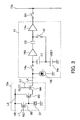
- Fig. 3 is a view showing the structure of the amplifier/noise cancel circuit 14.
- the amplifier/noise cancel circuit 14 includes a CDS circuit for canceling noise of fixed patterns included in image signals.
- a sample and hold switch 14a for controlling image signals input from the column selection signal line L4 is located in the amplifier/noise cancel circuit 14.
- a constant current source 14b for outputting constant current I is connected to the point where the sample and hold switch 14a and the column selection signal line L4 connect.
- a sample and hold capacitor C1 for holding a signal is connected to the output side of the sample and hold switch 14a.
- a reference voltage source 14c for supplying reference voltage VREF is connected to the other side of the sample and hold capacitor C1.
- a CDS capacitor C2 is connected to an output terminal of the amplifier 14d and the other side of the CDS capacitor C2 is connected to an input terminal of an amplifier 14e.
- the point where the sample and hold capacitor C1 and the reference voltage source 14c connect is connected via a clamping switch 14f to the point where the CDS capacitor C2 and the amplifier 14e connect.
- the clamping switch 14f By turning the clamping switch 14f to ON or OFF, the potential of a terminal on the amplifier 14e side of the CDS capacitor C2 can be fixed at reference voltage VREF supplied from the reference voltage source 14c or be separated from the reference voltage VREF.
- An output terminal of the amplifier 14e is connected to the output bus 15a via the column selection transistor M1.
- reset noise will be produced when a reset signal RST input to the reset transistor M2 goes into the OFF state.
- threshold voltage VT for the reset transistors M2
- reset noise produced in each pixel circuit 12a is not constant.
- the CDS circuit included in the amplifier/noise cancel circuit 14 is used to reliably remove such reset noise from output signals. This CDS circuit removes reset noise by sampling image signals from the pixel circuit 12a including reset noise, by sampling again voltage output at the time of a reset, and by obtaining differential signals.
- a row selection signal SLCT is input to the gate electrode on the row selection transistor M4 in the pixel circuit 12a.
- a reset signal RST is input with the row selection transistor M4 kept in the ON state to put the reset transistor M2 into the ON state.
- the photodiode D1 is reset to reset voltage VR and the reset voltage VR is output to the column selection signal line L4. The above operation will be performed during a horizontal blanking period.
- the clamping switch 14f and the sample and hold switch 14a are put into the ON state.
- the voltage of the image signals is applied to the point where the sample and hold capacitor C1 and the amplifier 14d connect, and image signals corresponding to integration time are accumulated in both the sample and hold capacitor C1 and the CDS capacitor C2 as electric charge .
- the signals accumulated at this time include reset noise.
- the clamping switch 14f and the sample and hold switch 14a are put into the OFF state to hold sampled image signals.
- a reset signal RST is input again to put the reset transistor M2 into the ON state.
- the photodiode D1 is reset to reset voltage VR and the reset voltage VR is output to the column selection signal line L4.
- the sample and hold switch 14a is put into the ON state, then the reset signal RST is put into the OFF state, and then the sample and hold switch 14a is also put into the OFF state after apredetermined period of time.
- GND potential will be obtained as constant potential by connecting a fixed potential wiring to an aluminum wiring for shading light located on the surface of a circuit area which light strikes.
- Fig. 4 is a plan view showing the positions in the CMOS image sensor 11 where fixed potential wirings are located.
- Fig. 4 is a view showing the whole of a semiconductor chip, on which the CMOS image sensor 11 is formed, looked at from the direction from which light strikes the chip.
- An area in Fig. 4 where slant lines are drawn is an aluminum wiring for shading light 21.
- the aluminum wiring for shading light 21 is formed so that it will cover the whole of the semiconductor chip, and it has an opening only in the middle.
- the pixel section 12 where the pixel circuits 12a are arranged like a matrix is formed in an area on the semiconductor chip corresponding to the opening to sense light which strikes the pixel section 12. Actually, a color filter will be formed on the aluminum wiring for shading light 21, but it is omitted in Fig. 4.
- An area of the color filter over the pixel section 12 transmits each of the RGB colors corresponding to each pixel circuit 12a.
- An area of the color filter over the aluminum wiring for shading light 21 is, for example, of unicolor black or of black obtained by mixing the RGB colors so that it will not transmit light.
- a cell 141 where the amplifier/noise cancel circuit 14 is formed is formed in an area shaded from light by the aluminum wiring for shading light 21. All the cells 141 in columns where the amplifier/noise cancel circuit 14 is formed have the same structure and are located parallel to one another to the arrangement of the pixel circuits 12a in a horizontal direction. Moreover, a fixed potential wiring 16 of aluminum is located between the cells 141 in adjacent columns where the amplifier/noise cancel circuit 14 is formed. The fixed potential wiring 16 in each column is connected to the aluminum wiring for shading light 21 by a contact hole 16a.
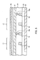
- Fig. 5 is a sectional view showing a first example of how to form the fixed potential wirings 16.
- Fig. 5 is an enlarged fragmentary sectional view taken along the line X-X of Fig. 4.
- a semiconductor chip where the CMOS image sensor 11 is formed has a multilayer structure.
- Signal transmission wirings 18 are formed over a power supply wiring 22 with an insulating layer 23 between.
- the aluminum wiring for shading light 21 is formed over the signal transmission wirings 18 with an insulating layer 24 between.
- a color filter 25 of, for example, black is located over the aluminum wiring for shading light 21.
- Power supply voltage VDD shared by circuits on this semiconductor chip is applied to the power supply wiring 22.
- the power supply wiring 22 will be located in, for example, a row direction (horizontal direction in Fig. 5).
- the aluminum wiring for shading light 21 is given GND potential in these circuits.
- the amplifier/noise cancel circuit 14 in each column is formed in an area 17 in Fig. 5. That is to say, in each area 17 in the example shown in Fig. 5, one signal transmission wiring 18 for transmitting image signals in a column direction is formed in the amplifier/noise cancel circuit 14 in each column.
- the signal transmission wiring 18 in Fig. 5 corresponds to a portion of the column selection signal line L4 which connects the source electrode on the row selection transistor M4 and the sample and hold switch 14a, a wiring which connects the sample and hold switch 14a and the sample and hold capacitor C1 and a wiring which connects the sample and hold switch 14a and the amplifier 14d, a wiring which connects the sample and hold capacitor C1 and the reference voltage source 14c, a wiring which connects the amplifier 14d and the CDS capacitor C2, a wiring which connects the CDS capacitor C2 and the amplifier 14e, or a portion of a wiring which connects the amplifier 14e and the column selection transistor M1 in the structure of the amplifier/noise cancel circuit 14 shown in Fig. 3.
- the fixed potential wiring 16 is formed between the signal transmission wirings 18 in columns.
- the fixed potential wirings 16 and the signal transmission wirings 18 are formed in the same wiring layer.
- the fixed potential wiring 16 is located in a column direction so that it will be parallel to adjacent signal transmission wirings 18.
- each fixed potential wiring 16 is connected to the aluminum wiring for shading light 21 by the contact hole 16a and is kept at GND potential.
- adjacent signal transmission wirings 18 are electrically shielded by the fixed potential wiring 16. This prevents image signals transmitted by adjacent signal transmission wirings 18 from interfering with each other. Distinct images therefore can be gotten without increasing power consumed by the CMOS image sensor 11 or without changing, for example, a capacitive element in the CMOS image sensor 11.
- the aluminum wiring for shading light 21 at GND potential is used. That is to say, by connecting the fixed potential wiring 16 and the aluminum wiring for shading light 21 by the contact hole 16a, constant potential can be applied to the fixed potential wiring 16 without changing the multilayer structure of semiconductor chips. As a result, a rise in manufacturing costs caused by forming the fixed potential wiring 16 can be prevented and an increase in the volume of semiconductor chips can be minimized.
- the amplifier/noise cancel circuit 14 in each column includes a CDS circuit. If space between CDS circuits in adjacent columns is narrow, the influence of interference on image signals will be especially great on wirings around capacitive elements located in the CDS circuits. If the structure of the amplifier/noise cancel circuit 14 shown in Fig. 3 is referred to, wirings connected to both ends of each of the sample and hold capacitor C1 and the CDS capacitor C2, being capacitive elements, may be formed in a column direction. In these areas, it is preferable that the fixed potential wiring 16 should be formed between wirings in adjacent columns. This willmaximizetheeffectofpreventingsignalinterferencebetween adjacent pixels.
- one signal transmission wiring 18 which extends in a column direction is located in each area 17 where the amplifier/noise cancel circuit 14 in one column is formed. If a plurality of signal transmission wirings 18 are arranged in the same wiring layer in each area 17, then the fixed potential wiring 16 should be formed in the same way in the same wiring layer between the areas 17. In this case, the fixed potential wiring 16 may also be formed between the signal transmission wirings 18 arranged.
- the aluminum wiring for shading light 21 at GND potential is used to keep the potential of the fixed potential wiring 16 constant. If the power supply wiring 22 is formed near the fixed potential wiring 16 as in the example shown in Fig. 5, the fixed potential wiring 16 may be connected to the power supply wiring 22 to get constant potential.
- Fig. 6 is a sectional view showing a second example of how to form fixed potential wirings.
- Fig. 6 is a fragmentary sectional view of a semiconductor chip showing a portion around an area 37 where the amplifier/noise cancel circuit 14 is formed. This is the same with Fig. 5.
- the multilayer structure of this semiconductor chip is as follows. A power supply wiring 42, insulating layers 43 and 44, and an aluminum wiring for shading light 41 are formed from the bottom in that order. This is the same with Fig. 5. Moreover, a color filter 45 of black is located over the aluminum wiring for shading light 41.
- Signal transmission wirings 38 are formed between the insulating layers 43 and 44 in each area 37 where the amplifier/noise cancel circuit 14 in a column is formed. In this case, two signal transmission wirings 38 are formed parallel to each other in the same wiring layer in the area 37 in each column.
- Fixed potential wirings 36 are formed not only between the areas 37 where the amplifier/noise cancel circuit 14 in each column is formed but also between the signal transmission wirings 38 arranged in each area 37. This prevents image signal interference not only between columns but also between wirings intheamplifier/noise cancel circuits 14 in columns. As aresult, images of higher quality can be gotten.
- each fixed potential wiring 36 is connected to the power supply wiring 42 by a contact hole 36a to get power supply voltage VDD as constant potential.
- the power supply voltage VDD is shared in this semiconductor chip, so there are many cases in which the power supply wiring 42 is also formed near the area 37 where the amplifier/noise cancel circuit 14 is formed. In these cases, the power supply wiring 42 and the fixed potential wiring 36 should be connected by the contact hole 36a. By doing so, constant potential can be applied to the fixed potential wiring 36 without changing the multilayer structure of a semiconductor chip. This is the same with the example shown in Fig. 5.
- signal transmission wirings are formed only in one wiring layer in an area where the amplifier/noise cancel circuit 14 is formed, but in reality there are many cases in which an area where signal transmission wirings are formed in a plurality of wiring layers exists. In these cases, fixed potential wirings should be formed parallel to signal transmission wirings so that they will correspond to the positions where the signal transmission wirings in each wiring layer are formed.
- the aluminum wiring for shading light 21 and the power supply wiring 42 connected to the fixed potential wirings 16 and 36 respectively are wirings for supplying voltage shared in a semiconductor chip, so their potential may vary according to conditions in the semiconductor chip.
- the potential of the fixed potential wirings 16 and 36 will also vary according to variation in the potential of these wirings. Therefore, variation in the potential of the fixed potential wirings 16 and 36 may influence the signal transmission wirings 18 and 38 adjacent to the fixed potential wirings 16 and 36 respectively and transmitted image signals may include noise.
- constant voltage should be supplied to the fixed potential wirings 16 and 36 via an independent dedicated wiring separated at a wiring pad located on the semiconductor chip.
- constant voltage should be supplied to the fixed potential wirings 16 and 36 from an independent voltage source located outside the semiconductor chip.
- reference voltage VREF supplied into the amplifier/noise cancel circuit 14 may also be supplied to the fixed potential wirings 16 and 36.
- CMOS image sensor As has been described in the foregoing, with a CMOS image sensor according to an embodiment of the present invent ion signal processing circuits are located parallel to one another and each of fixed potential wirings parallel to one another is located between two of the signal processing circuits. As a result, adjacent signal processing circuits are electrically shielded by a fixed potential wiring. This prevents image signals transmitted in adjacent signal processing circuits from interfering with each other. Therefore, distinct images can be gotten without increasing consumption of power or changing an element in a circuit.
Landscapes
- Engineering & Computer Science (AREA)
- Multimedia (AREA)
- Signal Processing (AREA)
- Solid State Image Pick-Up Elements (AREA)
- Transforming Light Signals Into Electric Signals (AREA)
Applications Claiming Priority (2)
| Application Number | Priority Date | Filing Date | Title |
|---|---|---|---|
| JP2002027277 | 2002-02-04 | ||
| JP2002027277A JP3992504B2 (ja) | 2002-02-04 | 2002-02-04 | Cmosイメージセンサ |
Publications (2)
| Publication Number | Publication Date |
|---|---|
| EP1333662A2 true EP1333662A2 (de) | 2003-08-06 |
| EP1333662A3 EP1333662A3 (de) | 2004-01-07 |
Family
ID=19192400
Family Applications (1)
| Application Number | Title | Priority Date | Filing Date |
|---|---|---|---|
| EP02258331A Withdrawn EP1333662A3 (de) | 2002-02-04 | 2002-12-03 | CMOS Bildsensor |
Country Status (6)
| Country | Link |
|---|---|
| US (1) | US7113215B2 (de) |
| EP (1) | EP1333662A3 (de) |
| JP (1) | JP3992504B2 (de) |
| KR (1) | KR100858452B1 (de) |
| CN (1) | CN1301004C (de) |
| TW (1) | TW569441B (de) |
Cited By (1)
| Publication number | Priority date | Publication date | Assignee | Title |
|---|---|---|---|---|
| WO2008060124A3 (en) * | 2006-11-17 | 2008-08-28 | Silicon Comm Technology Co Ltd | Low power image sensor adjusting reference voltage automatically and optical pointing device comprising the same |
Families Citing this family (35)
| Publication number | Priority date | Publication date | Assignee | Title |
|---|---|---|---|---|
| JP3183390B2 (ja) | 1995-09-05 | 2001-07-09 | キヤノン株式会社 | 光電変換装置及びそれを用いた撮像装置 |
| JP3972302B2 (ja) * | 2003-03-26 | 2007-09-05 | ソニー株式会社 | 撮像素子 |
| US20050200730A1 (en) * | 2004-03-11 | 2005-09-15 | Beck Jeffery S. | Active pixel sensor array sampling system and method |
| US7388608B2 (en) * | 2004-03-11 | 2008-06-17 | Micron Technology, Inc. | Sample and hold circuit and active pixel sensor array sampling system utilizing same |
| JP4352964B2 (ja) * | 2004-03-29 | 2009-10-28 | 株式会社島津製作所 | 二次元像検出器 |
| JP2006019927A (ja) * | 2004-06-30 | 2006-01-19 | Fujitsu Ltd | kTC雑音を低減したCMOSイメージセンサ、同イメージセンサの用いるリセットトランジスタ制御回路、および同制御回路に用いる電圧切替回路 |
| JP4969771B2 (ja) * | 2004-07-12 | 2012-07-04 | ソニー株式会社 | 固体撮像装置及びそのキャパシタ調整方法 |
| CN100446547C (zh) * | 2005-03-07 | 2008-12-24 | 富士胶片株式会社 | 具有扩大面积的光电管的固态图像传感器 |
| KR100729501B1 (ko) * | 2005-08-03 | 2007-06-15 | 매그나칩 반도체 유한회사 | 자동초점조절 기능을 갖는 cmos 이미지센서 및 그를포함하는 카메라 장치 |
| US7919827B2 (en) * | 2005-03-11 | 2011-04-05 | Taiwan Semiconductor Manufacturing Co., Ltd. | Method and structure for reducing noise in CMOS image sensors |
| US7573519B2 (en) * | 2005-10-26 | 2009-08-11 | Eastman Kodak Company | Method for correcting eclipse or darkle |
| JP4144892B2 (ja) | 2006-08-28 | 2008-09-03 | キヤノン株式会社 | 光電変換装置及び撮像装置 |
| US20080308585A1 (en) * | 2006-09-27 | 2008-12-18 | John Foley | Nozzle |
| JP2008108917A (ja) * | 2006-10-25 | 2008-05-08 | Sony Corp | 固体撮像装置及び電子機器 |
| US7537951B2 (en) | 2006-11-15 | 2009-05-26 | International Business Machines Corporation | Image sensor including spatially different active and dark pixel interconnect patterns |
| JP5067011B2 (ja) * | 2007-05-18 | 2012-11-07 | ソニー株式会社 | 固体撮像装置、撮像装置、電子機器 |
| CN101387771B (zh) * | 2007-09-14 | 2010-08-18 | 群康科技(深圳)有限公司 | 液晶显示装置 |
| TWI359611B (en) * | 2008-02-21 | 2012-03-01 | Novatek Microelectronics Corp | Image sensor capable of reducing noises |
| JP5173503B2 (ja) * | 2008-03-14 | 2013-04-03 | キヤノン株式会社 | 撮像装置及び撮像システム |
| JP5006281B2 (ja) * | 2008-07-24 | 2012-08-22 | パナソニック株式会社 | 固体撮像装置、カメラ |
| JP2010225618A (ja) * | 2009-03-19 | 2010-10-07 | Seiko Epson Corp | センシング装置および電子機器 |
| US8624875B2 (en) * | 2009-08-24 | 2014-01-07 | Semiconductor Energy Laboratory Co., Ltd. | Method for driving touch panel |
| WO2011055638A1 (en) | 2009-11-06 | 2011-05-12 | Semiconductor Energy Laboratory Co., Ltd. | Display device |
| JP5578008B2 (ja) * | 2010-10-12 | 2014-08-27 | ソニー株式会社 | 固体撮像装置、固体撮像装置の駆動方法および撮像装置 |
| CA2835870A1 (en) | 2011-05-12 | 2012-11-15 | Olive Medical Corporation | Pixel array area optimization using stacking scheme for hybrid image sensor with minimal vertical interconnects |
| JP6239820B2 (ja) * | 2011-12-19 | 2017-11-29 | キヤノン株式会社 | 撮像装置及びその制御方法 |
| CN104486987A (zh) | 2012-07-26 | 2015-04-01 | 橄榄医疗公司 | 具有最小面积单片式cmos图像传感器的相机系统 |
| WO2014145246A1 (en) | 2013-03-15 | 2014-09-18 | Olive Medical Corporation | Image sensor synchronization without input clock and data transmission clock |
| AU2014233192B2 (en) | 2013-03-15 | 2018-11-22 | DePuy Synthes Products, Inc. | Minimize image sensor I/O and conductor counts in endoscope applications |
| US10694131B2 (en) | 2016-06-15 | 2020-06-23 | Samsung Electronics Co., Ltd. | Comparing circuit and an image sensor including a current stabilization circuit |
| JP7452962B2 (ja) * | 2018-11-16 | 2024-03-19 | ソニーセミコンダクタソリューションズ株式会社 | 撮像装置 |
| FR3102885B1 (fr) * | 2019-10-31 | 2022-03-18 | Trixell | Capteur photosensible à capteurs élémentaires raboutés |
| CN111430394A (zh) * | 2020-04-26 | 2020-07-17 | 上海微阱电子科技有限公司 | 一种图像传感器结构及制作方法 |
| JP7678676B2 (ja) | 2021-02-04 | 2025-05-16 | キヤノン株式会社 | 光電変換装置 |
| JP7676159B2 (ja) * | 2021-02-04 | 2025-05-14 | キヤノン株式会社 | 光電変換装置 |
Citations (7)
| Publication number | Priority date | Publication date | Assignee | Title |
|---|---|---|---|---|
| US5065171A (en) | 1989-10-04 | 1991-11-12 | Fuji Xerox Co., Ltd. | Image sensor with uniformly dispersed storage capacitors |
| US5122649A (en) | 1989-12-11 | 1992-06-16 | Fuji Photo Film Co., Ltd. | Solid-state imaging device having a predetermined impurity layer embedded between two adjacent sets of switching transistors |
| US5136358A (en) | 1990-06-06 | 1992-08-04 | Fuji Xerox Co., Ltd. | Multi-layered wiring structure |
| US5151380A (en) * | 1991-08-19 | 1992-09-29 | Texas Instruments Incorporated | Method of making top buss virtual phase frame interline transfer CCD image sensor |
| EP0917205A2 (de) * | 1997-11-11 | 1999-05-19 | Nec Corporation | CMOS Bildsensor mit hoher Ausgangsleistung |
| US6201573B1 (en) | 1995-11-13 | 2001-03-13 | Hamamatsu Photonics K. K. | Solid state imaging apparatus for imaging a two dimensional optical image having a number of integration circuits |
| EP1176808A2 (de) * | 2000-07-27 | 2002-01-30 | Canon Kabushiki Kaisha | Bildaufnahmevorrichtung |
Family Cites Families (8)
| Publication number | Priority date | Publication date | Assignee | Title |
|---|---|---|---|---|
| KR100464955B1 (ko) * | 1998-06-29 | 2005-04-06 | 매그나칩 반도체 유한회사 | 메모리소자와 함께 집적화된 씨모스 이미지센서 |
| JP4812940B2 (ja) * | 1998-10-30 | 2011-11-09 | 浜松ホトニクス株式会社 | 固体撮像装置アレイ |
| KR20010061308A (ko) * | 1999-12-28 | 2001-07-07 | 박종섭 | 박막 이미지센서의 제조 방법 |
| KR100429571B1 (ko) * | 1999-12-28 | 2004-05-03 | 주식회사 하이닉스반도체 | 저전력화 및 화질 개선을 위한 단위 화소 회로 및 판독 회로를 갖는 이미지센서 |
| KR100320439B1 (ko) * | 1999-12-30 | 2002-01-12 | 박종섭 | 씨모스 이미지 센서 |
| US6452149B1 (en) * | 2000-03-07 | 2002-09-17 | Kabushiki Kaisha Toshiba | Image input system including solid image sensing section and signal processing section |
| KR20010087810A (ko) * | 2001-06-11 | 2001-09-26 | 하경호 | 근접 센싱을 위한 고집적 cmos 이미지 센서 |
| US6927433B2 (en) * | 2001-06-28 | 2005-08-09 | Isetec, Inc | Active pixel image sensor with two transistor pixel, in-pixel non-uniformity correction, and bootstrapped reset lines |
-
2002
- 2002-02-04 JP JP2002027277A patent/JP3992504B2/ja not_active Expired - Fee Related
- 2002-12-03 EP EP02258331A patent/EP1333662A3/de not_active Withdrawn
- 2002-12-03 TW TW091135083A patent/TW569441B/zh not_active IP Right Cessation
- 2002-12-16 US US10/319,516 patent/US7113215B2/en not_active Expired - Fee Related
- 2002-12-17 KR KR1020020080579A patent/KR100858452B1/ko not_active Expired - Fee Related
- 2002-12-24 CN CNB021570612A patent/CN1301004C/zh not_active Expired - Fee Related
Patent Citations (7)
| Publication number | Priority date | Publication date | Assignee | Title |
|---|---|---|---|---|
| US5065171A (en) | 1989-10-04 | 1991-11-12 | Fuji Xerox Co., Ltd. | Image sensor with uniformly dispersed storage capacitors |
| US5122649A (en) | 1989-12-11 | 1992-06-16 | Fuji Photo Film Co., Ltd. | Solid-state imaging device having a predetermined impurity layer embedded between two adjacent sets of switching transistors |
| US5136358A (en) | 1990-06-06 | 1992-08-04 | Fuji Xerox Co., Ltd. | Multi-layered wiring structure |
| US5151380A (en) * | 1991-08-19 | 1992-09-29 | Texas Instruments Incorporated | Method of making top buss virtual phase frame interline transfer CCD image sensor |
| US6201573B1 (en) | 1995-11-13 | 2001-03-13 | Hamamatsu Photonics K. K. | Solid state imaging apparatus for imaging a two dimensional optical image having a number of integration circuits |
| EP0917205A2 (de) * | 1997-11-11 | 1999-05-19 | Nec Corporation | CMOS Bildsensor mit hoher Ausgangsleistung |
| EP1176808A2 (de) * | 2000-07-27 | 2002-01-30 | Canon Kabushiki Kaisha | Bildaufnahmevorrichtung |
Cited By (3)
| Publication number | Priority date | Publication date | Assignee | Title |
|---|---|---|---|---|
| WO2008060124A3 (en) * | 2006-11-17 | 2008-08-28 | Silicon Comm Technology Co Ltd | Low power image sensor adjusting reference voltage automatically and optical pointing device comprising the same |
| CN102065248B (zh) * | 2006-11-17 | 2013-03-20 | 硅通讯技术有限公司 | 自动调节参考电压的低功耗图像传感器以及包含此传感器的光学点击装置 |
| US8604406B2 (en) | 2006-11-17 | 2013-12-10 | Silicon Communications Technology Co., Ltd | Low power image sensor adjusting reference voltage automatically and optical pointing device comprising the same |
Also Published As
| Publication number | Publication date |
|---|---|
| CN1301004C (zh) | 2007-02-14 |
| TW569441B (en) | 2004-01-01 |
| US20030146994A1 (en) | 2003-08-07 |
| EP1333662A3 (de) | 2004-01-07 |
| US7113215B2 (en) | 2006-09-26 |
| JP2003229557A (ja) | 2003-08-15 |
| TW200303088A (en) | 2003-08-16 |
| CN1437387A (zh) | 2003-08-20 |
| KR100858452B1 (ko) | 2008-09-16 |
| JP3992504B2 (ja) | 2007-10-17 |
| KR20030066308A (ko) | 2003-08-09 |
Similar Documents
| Publication | Publication Date | Title |
|---|---|---|
| US7113215B2 (en) | CMOS image sensor | |
| JP3467013B2 (ja) | 固体撮像装置 | |
| EP0862219B1 (de) | Aktiver Bildsensor, bei dem zwei benachbarte Bildelemente ein gemeinsames elektrisches integriertes Element teilen | |
| US7663168B2 (en) | Image pickup element performing image detection of high resolution and high image quality and image pickup apparatus including the same | |
| JP5154908B2 (ja) | Cmosイメージセンサのための、小サイズ、高利得及び低ノイズのピクセル | |
| US7688373B2 (en) | Solid-state imaging device with specific contact arrangement | |
| US9293503B2 (en) | Solid-state imaging device, method for driving the same, method for manufacturing the same, and electronic device | |
| US8284283B2 (en) | Amplification type solid state imaging device | |
| US9621832B2 (en) | Solid-state image sensor and camera | |
| US7656449B2 (en) | Solid-state imaging apparatus having gate potential that is negtive with respect to a well region | |
| US20070109437A1 (en) | Solid state image sensing device | |
| US6137151A (en) | Amorphous silicon sensor array with reduced number of address lines | |
| US7432964B2 (en) | Solid-state imaging device with plural CDS circuits per column sharing a capacitor and/or clamping transistor | |
| KR100830583B1 (ko) | 듀얼 캡쳐가 가능한 씨모스 이미지 센서의 픽셀 회로 및그것의 구조 | |
| US7202899B2 (en) | Method to prevent white pixels in a CMOS image sensor | |
| JP2006210468A (ja) | 固体撮像装置 |
Legal Events
| Date | Code | Title | Description |
|---|---|---|---|
| PUAI | Public reference made under article 153(3) epc to a published international application that has entered the european phase |
Free format text: ORIGINAL CODE: 0009012 |
|
| AK | Designated contracting states |
Designated state(s): AT BE BG CH CY CZ DE DK EE ES FI FR GB GR IE IT LI LU MC NL PT SE SI SK TR |
|
| AX | Request for extension of the european patent |
Extension state: AL LT LV MK RO |
|
| PUAL | Search report despatched |
Free format text: ORIGINAL CODE: 0009013 |
|
| AK | Designated contracting states |
Kind code of ref document: A3 Designated state(s): AT BE BG CH CY CZ DE DK EE ES FI FR GB GR IE IT LI LU MC NL PT SE SI SK TR |
|
| AX | Request for extension of the european patent |
Extension state: AL LT LV MK RO |
|
| RIC1 | Information provided on ipc code assigned before grant |
Ipc: 7H 01L 27/146 B Ipc: 7H 04N 3/15 A Ipc: 7H 04N 5/335 B |
|
| 17P | Request for examination filed |
Effective date: 20040630 |
|
| AKX | Designation fees paid |
Designated state(s): DE FR GB IT |
|
| RAP1 | Party data changed (applicant data changed or rights of an application transferred) |
Owner name: FUJITSU MICROELECTRONICS LIMITED |
|
| RAP1 | Party data changed (applicant data changed or rights of an application transferred) |
Owner name: FUJITSU SEMICONDUCTOR LIMITED |
|
| 17Q | First examination report despatched |
Effective date: 20101222 |
|
| RAP1 | Party data changed (applicant data changed or rights of an application transferred) |
Owner name: SOCIONEXT INC. |
|
| RIC1 | Information provided on ipc code assigned before grant |
Ipc: H04N 5/363 20110101ALI20170630BHEP Ipc: H04N 5/357 20110101ALI20170630BHEP Ipc: H01L 27/146 20060101ALI20170630BHEP Ipc: H04N 5/335 20110101AFI20170630BHEP |
|
| GRAP | Despatch of communication of intention to grant a patent |
Free format text: ORIGINAL CODE: EPIDOSNIGR1 |
|
| INTG | Intention to grant announced |
Effective date: 20170922 |
|
| STAA | Information on the status of an ep patent application or granted ep patent |
Free format text: STATUS: THE APPLICATION IS DEEMED TO BE WITHDRAWN |
|
| 18D | Application deemed to be withdrawn |
Effective date: 20180203 |