EP1339095A2 - Procédé de découpe d'un ruban de protection et dispositif d'application de ruban de protection - Google Patents
Procédé de découpe d'un ruban de protection et dispositif d'application de ruban de protection Download PDFInfo
- Publication number
- EP1339095A2 EP1339095A2 EP20030000966 EP03000966A EP1339095A2 EP 1339095 A2 EP1339095 A2 EP 1339095A2 EP 20030000966 EP20030000966 EP 20030000966 EP 03000966 A EP03000966 A EP 03000966A EP 1339095 A2 EP1339095 A2 EP 1339095A2
- Authority
- EP
- European Patent Office
- Prior art keywords
- protective tape
- tape
- cutting
- cutter
- blade edge
- Prior art date
- Legal status (The legal status is an assumption and is not a legal conclusion. Google has not performed a legal analysis and makes no representation as to the accuracy of the status listed.)
- Withdrawn
Links
Images


Classifications
-
- H—ELECTRICITY
- H10—SEMICONDUCTOR DEVICES; ELECTRIC SOLID-STATE DEVICES NOT OTHERWISE PROVIDED FOR
- H10P—GENERIC PROCESSES OR APPARATUS FOR THE MANUFACTURE OR TREATMENT OF DEVICES COVERED BY CLASS H10
- H10P52/00—Grinding, lapping or polishing of wafers, substrates or parts of devices
-
- H—ELECTRICITY
- H10—SEMICONDUCTOR DEVICES; ELECTRIC SOLID-STATE DEVICES NOT OTHERWISE PROVIDED FOR
- H10P—GENERIC PROCESSES OR APPARATUS FOR THE MANUFACTURE OR TREATMENT OF DEVICES COVERED BY CLASS H10
- H10P72/00—Handling or holding of wafers, substrates or devices during manufacture or treatment thereof
- H10P72/04—Apparatus for manufacture or treatment
- H10P72/0442—Apparatus for placing on an insulating substrate, e.g. tape
-
- H—ELECTRICITY
- H10—SEMICONDUCTOR DEVICES; ELECTRIC SOLID-STATE DEVICES NOT OTHERWISE PROVIDED FOR
- H10P—GENERIC PROCESSES OR APPARATUS FOR THE MANUFACTURE OR TREATMENT OF DEVICES COVERED BY CLASS H10
- H10P72/00—Handling or holding of wafers, substrates or devices during manufacture or treatment thereof
- H10P72/04—Apparatus for manufacture or treatment
- H10P72/0428—Apparatus for mechanical treatment or grinding or cutting
-
- Y—GENERAL TAGGING OF NEW TECHNOLOGICAL DEVELOPMENTS; GENERAL TAGGING OF CROSS-SECTIONAL TECHNOLOGIES SPANNING OVER SEVERAL SECTIONS OF THE IPC; TECHNICAL SUBJECTS COVERED BY FORMER USPC CROSS-REFERENCE ART COLLECTIONS [XRACs] AND DIGESTS
- Y10—TECHNICAL SUBJECTS COVERED BY FORMER USPC
- Y10T—TECHNICAL SUBJECTS COVERED BY FORMER US CLASSIFICATION
- Y10T156/00—Adhesive bonding and miscellaneous chemical manufacture
- Y10T156/10—Methods of surface bonding and/or assembly therefor
- Y10T156/1052—Methods of surface bonding and/or assembly therefor with cutting, punching, tearing or severing
- Y10T156/108—Flash, trim or excess removal
-
- Y—GENERAL TAGGING OF NEW TECHNOLOGICAL DEVELOPMENTS; GENERAL TAGGING OF CROSS-SECTIONAL TECHNOLOGIES SPANNING OVER SEVERAL SECTIONS OF THE IPC; TECHNICAL SUBJECTS COVERED BY FORMER USPC CROSS-REFERENCE ART COLLECTIONS [XRACs] AND DIGESTS
- Y10—TECHNICAL SUBJECTS COVERED BY FORMER USPC
- Y10T—TECHNICAL SUBJECTS COVERED BY FORMER US CLASSIFICATION
- Y10T156/00—Adhesive bonding and miscellaneous chemical manufacture
- Y10T156/10—Methods of surface bonding and/or assembly therefor
- Y10T156/1052—Methods of surface bonding and/or assembly therefor with cutting, punching, tearing or severing
- Y10T156/1084—Methods of surface bonding and/or assembly therefor with cutting, punching, tearing or severing of continuous or running length bonded web
- Y10T156/1085—One web only
-
- Y—GENERAL TAGGING OF NEW TECHNOLOGICAL DEVELOPMENTS; GENERAL TAGGING OF CROSS-SECTIONAL TECHNOLOGIES SPANNING OVER SEVERAL SECTIONS OF THE IPC; TECHNICAL SUBJECTS COVERED BY FORMER USPC CROSS-REFERENCE ART COLLECTIONS [XRACs] AND DIGESTS
- Y10—TECHNICAL SUBJECTS COVERED BY FORMER USPC
- Y10T—TECHNICAL SUBJECTS COVERED BY FORMER US CLASSIFICATION
- Y10T156/00—Adhesive bonding and miscellaneous chemical manufacture
- Y10T156/12—Surface bonding means and/or assembly means with cutting, punching, piercing, severing or tearing
- Y10T156/1317—Means feeding plural workpieces to be joined
- Y10T156/1343—Cutting indefinite length web after assembly with discrete article
-
- Y—GENERAL TAGGING OF NEW TECHNOLOGICAL DEVELOPMENTS; GENERAL TAGGING OF CROSS-SECTIONAL TECHNOLOGIES SPANNING OVER SEVERAL SECTIONS OF THE IPC; TECHNICAL SUBJECTS COVERED BY FORMER USPC CROSS-REFERENCE ART COLLECTIONS [XRACs] AND DIGESTS
- Y10—TECHNICAL SUBJECTS COVERED BY FORMER USPC
- Y10T—TECHNICAL SUBJECTS COVERED BY FORMER US CLASSIFICATION
- Y10T156/00—Adhesive bonding and miscellaneous chemical manufacture
- Y10T156/12—Surface bonding means and/or assembly means with cutting, punching, piercing, severing or tearing
- Y10T156/1348—Work traversing type
-
- Y—GENERAL TAGGING OF NEW TECHNOLOGICAL DEVELOPMENTS; GENERAL TAGGING OF CROSS-SECTIONAL TECHNOLOGIES SPANNING OVER SEVERAL SECTIONS OF THE IPC; TECHNICAL SUBJECTS COVERED BY FORMER USPC CROSS-REFERENCE ART COLLECTIONS [XRACs] AND DIGESTS
- Y10—TECHNICAL SUBJECTS COVERED BY FORMER USPC
- Y10T—TECHNICAL SUBJECTS COVERED BY FORMER US CLASSIFICATION
- Y10T156/00—Adhesive bonding and miscellaneous chemical manufacture
- Y10T156/17—Surface bonding means and/or assemblymeans with work feeding or handling means
- Y10T156/1702—For plural parts or plural areas of single part
- Y10T156/1712—Indefinite or running length work
- Y10T156/1734—Means bringing articles into association with web
-
- Y—GENERAL TAGGING OF NEW TECHNOLOGICAL DEVELOPMENTS; GENERAL TAGGING OF CROSS-SECTIONAL TECHNOLOGIES SPANNING OVER SEVERAL SECTIONS OF THE IPC; TECHNICAL SUBJECTS COVERED BY FORMER USPC CROSS-REFERENCE ART COLLECTIONS [XRACs] AND DIGESTS
- Y10—TECHNICAL SUBJECTS COVERED BY FORMER USPC
- Y10T—TECHNICAL SUBJECTS COVERED BY FORMER US CLASSIFICATION
- Y10T83/00—Cutting
- Y10T83/04—Processes
- Y10T83/05—With reorientation of tool between cuts
-
- Y—GENERAL TAGGING OF NEW TECHNOLOGICAL DEVELOPMENTS; GENERAL TAGGING OF CROSS-SECTIONAL TECHNOLOGIES SPANNING OVER SEVERAL SECTIONS OF THE IPC; TECHNICAL SUBJECTS COVERED BY FORMER USPC CROSS-REFERENCE ART COLLECTIONS [XRACs] AND DIGESTS
- Y10—TECHNICAL SUBJECTS COVERED BY FORMER USPC
- Y10T—TECHNICAL SUBJECTS COVERED BY FORMER US CLASSIFICATION
- Y10T83/00—Cutting
- Y10T83/04—Processes
- Y10T83/0605—Cut advances across work surface
Definitions
- the present invention relates to a technique of cutting a protective tape applied onto the surface of semiconductor wafer on which a pattern is formed.
- wafer back surface of semiconductor wafer
- the methods include mechanical process such as grinding or polishing, or chemical process such as etching.
- a protective tape is applied onto the surface of wafer in order to protect the surface of the wafer having wiring patter thereon.
- the protective tape is applied in the following manner.
- a protective tape is applied onto the surface of the wafer sucked and held on a chuck table, thereafter, the protective tape applied onto the wafer is cut along the outline of the wafer by a cutter unit.
- the blade edge of the cutter unit contacting with the protective tape has a specified portion always repeatedly used.
- the protective tape is cut, thereafter, unwanted tape is separated and collected, and the work for applying the protective tape is completed.
- the hard and thick protective tape is cut, and thereby, the edge of the cutter contacting with the protective tape early wears; as a result, sharpness of the blade is early lost.
- the work for cutting the protective tape applied onto the wafer is continued, thrust increases in cutting, and stress by the thrust is applied to the wafer. As a result, there is a problem of breaking down the wafer.
- the present invention has been proposed in view of the above circumstances. It is, therefore, a principal object of the present invention to provide a method of cutting a protective tape, which can continuously and effectively apply a protective tape onto the surface of semiconductor wafer. Another object of the present invention is to provide a protective tape applying apparatus employing the method same as above.
- a method of cutting a protective tape applied on a surface of semiconductor wafer along an outline of the semiconductor wafer by a cutter comprising:
- the contact portion of the blade edge of the cutter is displaced. Therefore, even if the sharpness of specified blade edge portions is lost, it is possible to cut the protective tape using other sharp blade edge portions. This serves to reduce the stress by thrust applied to the semiconductor wafer when cutting the protective tape. As a result, the semiconductor wafer can be prevented from being broken down.
- the contact portion of the blade edge is displaced, and thereby, it is possible to cut the protective tape by one cutter for a long time. As a result, there is no need of frequently replacing the blade edge with a new blade edge; therefore, a working efficiency can be improved.
- the displacement of the contact portion of a blade edge of the cutter to the protective tape is set to a predetermined interval.
- the contact portion of a blade edge of the cutter to the protective tape is displaced while being vertically moving with the elapse.
- the interval setup of the contact portion of a blade edge of the cutter to the protective tape is made by vertically moving a cutter unit including the cutter and by vertically moving holding means for placing and holding the semiconductor wafer.
- the contact portion of the blade edge of the cutter to the protective tape during cutting of the protective tape is displaced with the elapse by vertically moving a cutter unit including the cutter and by vertically moving holding means for placing and holding the semiconductor wafer.
- the protective tape is applied onto the surface of the semiconductor wafer, thereafter, cut.
- the protective tape may comprise a single sheet, or may comprise a tape previously laminating the same or different kind of protective tapes.
- the protective tape may be cut into a shape having a diameter larger than an outer diameter of the semiconductor wafer.
- a protective tape applying apparatus for applying a protective tape onto a surface of semiconductor wafer, comprising:
- the protective tape is applied onto the surface of the semiconductor wafer held by the holding means.
- the protective tape is cut by the cutter unit by along the outline of the semiconductor wafer; in this case, the first control means controls the vertical movement of the cutter unit. Therefore, since the blade edge position of the cutter unit is set and changed by the first control means, the blade edge portion losing sharpness due to wear can be replaced with a sharp blade edge having no wear.
- the apparatus further includes second vertical drive means for vertically moving the holding means, and second control means for controlling the operation of the second vertical drive means so that a contact portion of a blade edge of the cutter unit to the protective tape can be displaced.
- the second control means controls the vertical movement of the holding means so that the contact portion of the blade edge of the cutter to the protective tape can be set and changed. Therefore, the blade edge portion losing sharpness due to wear can be replaced with a sharp blade edge having no wear.
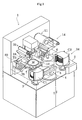
- Fig. 1 is a perspective view schematically showing the structure of a protective tape applying apparatus.
- a protective tape applying apparatus 1 for semiconductor wafer includes a wafer supplier 3 and a wafer collector 34.
- the wafer supplier 3 is arranged at the left of the near side of a base plate 2, and is loaded with a cassette C1 storing wafers W.
- the wafer collector 34 is arranged at the right of the same as above, and is used to collect wafers W with a protective tape T1 applied on the surface.
- a wafer transport mechanism 4 is interposed between the wafer supplier 3 and the wafer collector 34.
- the base plate 2 is provided with an alignment stage 6 at the right of the far side.
- a tape server 11 for supplying the protective tape T1 to the wafer W is provided above the alignment state 6.
- a separator collector 14 is arranged on the obliquely right side under the tape server 11.
- the separator collector 14 collects only separator from the protective tape T1 with separator supplied from the tape server 11.
- a chuck table 7, a tape applying mechanism 16 and a tape separating mechanism 30 are arranged on the left side of the alignment stage 6.
- the chuck table 7 sucks and holds the wafer W, and the tape applying mechanism 16 applies the protective tape T1 onto the wafer W held on the chuck table 7.
- the tape separating mechanism 30 separates unwanted tape after the protective tape T1 is applied onto the wafer W.
- a cutter mechanism 18 is arranged above the tape separating mechanism 30. The cutter mechanism 18 cuts the protective tape T1 applied onto the wafer W along the outline of the wafer W.
- a tape collector 32 for collecting the unwanted tape is arranged above on the left side of the base plate 2.
- a static electricity eliminator 35 is arranged at the side opposite to the chuck table 7. The static electricity eliminator 35 eliminates static electricity from the protective tape before being applied onto the wafer W and unwanted tape T2 before being collected after the protective tape T1 applied onto the wafer W.
- the wafer supplier 3 includes a vertically movable cassette table, and the cassette C1 storing wafers in the multiple stage form is placed on the cassette table.
- the wafer W is horizontally kept in a state that the pattern surface is upwardly directed.
- the wafer transport mechanism 4 is provided with a robot arm 5, and is configured so that it can be rotated by a drive mechanism (not shown).
- the robot arm 5 includes a horseshoe-shaped wafer retainer at the distal end.
- the wafer retainer is formed with a suction hole (not shown) so that the wafer W can be vacuum-sucked from the back side.
- the robot arm 5 sucks and holds the wafer W from the back side in a manner that the wafer retainer is inserted into the clearance between wafers W stored in the cassette C1 in the multiple stage form. Further, the robot arm 5 carries the sucked and held wafer W in the order of the alignment stage 6, chuck table 7 and wafer collector 34, which will be described later.
- the alignment stage 6 performs the alignment of the placed wafer W based on orientation flat.
- the chuck table 7 performs the alignment based on orientation flat of the transferred and placed wafer W, and fully covers the back surface of the wafer W so that the wafer W can be vacuum-sucked. Namely, the chuck table 7 is formed with suction holes 8 at the outer peripheral portion and the central portion, as seen from Fig. 2.
- the chuck table 7 is formed with grooves 9 into which a blade edge 25 of the cutter unit 20 described later is inserted in order to cut the protective tape T1 along the outline of the wafer W.
- a plurality of grooves 9 is formed correspondingly to the outline of the wafer having different size.
- a wide groove 10 is formed along the radius direction of the chuck table 7 at the initial position (left-handed near side in Fig. 2) of the grooves 9 into which the blade edge 25 of the cutter unit 20 is inserted.
- the groove 10 is connected with all of the above grooves 9.
- the chuck table 7 is equivalent to holding means of the present invention.
- the tape server 11 guides the protective tape T1 with separator S fed from a tape bobbin 12 while winding it around the group of guide rollers 13.
- the tape server 11 is rotatably supported to a longitudinal wall of the apparatus main body, and is controlled in its rotation via a break mechanism.
- the separator collector 14 includes a collector bobbin 15, which is rotatably supported to the longitudinal wall, and interlocked and connected with a drive mechanism such as a motor.
- the tape applying mechanism 16 is held on a rail of the apparatus main body so that the frame is slidable in the tape traveling (running) direction, and interlocked and connected with a drive mechanism (not shown).
- An applying roller 17 is rotatably supported to the frame, and is vertically swung by a cylinder (not shown).
- the applying roller 17 presses the surface of the protective tape T1 while rolling thereon so that the protective tape T1 can be applied onto the surface of the wafer W.
- the above tape applying mechanism 16 is equivalent to applying means of the present invention.
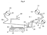
- the cutter mechanism 18 includes a cutter unit 20 (portion surrounded by a two-dotted chain line), a vertical drive section 28, and a control section 29, as shown in Fig. 3.
- the cutter unit 20 is attached to a ball shaft so that it is vertically movable.
- the vertical drive section 28 moves the cutter unit 20 in the vertical direction.
- the control section 29 controls the vertical drive section 28.
- the above cutter unit 20 comprises a vertically movable member 21, an arm 22, a motor 23, a rotatable arm 24, and a cutter blade edge 25.
- the arm 22 is supported to the vertically movable member 21 like cantilever bridge.
- the motor 23 is attached to the upper portion of the distal end of the arm 22.
- the arm 24 has one end connected to the rotary shaft of the motor 23, which downwardly extends and penetrates through the arm 22.
- the cutter blade edge 25 is attached downwardly to the other end of the arm 24.
- the vertically movable member 21 is vertically movable along the ball shaft 19.
- a stopper 26 is provided via a bottom plate 27 at the bottom portion of the ball shaft 19. The stopper 26 is used to control the lowest position (height) of the vertically movable member 21.
- the motor 23 transmits a moment of rotation to the arm 24 via the rotary shaft so that the arm 24 can be rotated.
- the stopper 3 is formed into a shape of screw, and is screwed into the bottom plate 27 so that the lowest position of the vertical movable member 21 can be adjusted.
- the stopped is not limited to the above shape of screw.
- the stopper may be of course other than forms so long as it can control the lowest position of the vertical movable member 21.
- the control section 29 controls the vertical drive section 28 so that the cutter unit 20 can be vertically moved between a standby position and the operating position of cutting the protective tape T1. Further, the control section 29 changes the contact portion of the protective tape T1 and the blade edge 25 of the cutter unit 20.
- the control section 29 and the vertical drive section 28 are equivalent to control means and vertically driving means, respectively.
- control section 29 displaces the contact portion of the blade edge 25 to the protective tape T1 at micro unit (interval).
- the control section 29 controls the blade edge 25 so that the protective tape T1 can be repeatedly cut successively using blade edge contact portions P1 to P5 preset with predetermined intervals.
- the contact portion may be properly modified depending on the number of cutting protective tapes corresponding to the kind of the protective tape.
- the tape separating mechanism 30 is held to a rail of the apparatus main body so that the frame is slidable in the tape traveling direction, and interlocked and connected via a drive mechanism such as a motor (not shown).
- a separating roller 31 is rotatably supported to the frame, and is vertically swung by a cylinder (not shown). The separating roller 31 is used to separate unwanted tape T2 after being cut along the outer periphery of the wafer W from the wafer W.
- a tape collector 32 includes a collector bobbin 33, which is rotatably supported to the longitudinal wall of the base plate, and interlocked and connected with a drive mechanism such as a motor. More specifically, when a predetermined amount of the protective tape T1 is fed from the tape server 11, and supplied onto the wafer W, the driving section is operated so that the unwanted tape T2 after cutting the protective tape T1 can be wound up the collector bobbin 33.
- the wafer collector 34 includes a vertically movable cassette table, and a cassette C2 is placed on the cassette table.
- the cassette C2 stores wafers having the protective tape applied on the surface in the multiple stage form. In this case, the wafer W is horizontally kept in a state that the pattern surface is upwardly directed.
- the cassette table is vertically moved, thereafter, stopped at the position capable of taking out a wafer, which is an object to be taken, by the robot arm 5.
- the wafer transport mechanism 4 is rotated so that the wafer retainer of the robot arm 5 can be inserted into the clearance between wafers stored in the cassette C1.
- the robot arm 5 takes out the wafer W in a state that the wafer retainer sucks and holds it from the back surface, and transfers the wafer W to the alignment stage 6.
- the wafer W placed on the alignment stage 6 is positioned based on orientation flat and notch. After positioning is completed, the wafer W is transferred onto the chuck table in a state of being sucked and held from the back surface by the robot arm 5.
- the wafer W placed on the chuck table 7 is positioned, thereafter, sucked and held.
- the tape applying mechanism 16 and the tape separating mechanism 30 are situated on the initial position (left side of the chuck table 7), and the cutter unit 20 is situated on the standby position (above tape applying mechanism 16).
- the alignment of the wafer W is completed, thereafter, the applying roller 17 of the tape applying mechanism 16 swung downward.
- the applying roller 17 rolls on the wafer W to a direction (from the left to the right in Fig. 6) reverse to the tape traveling direction while pressing down the protective tape T1. Therefore, the protective tape T1 can be uniformly applied to the entire surface of the wafer W. Thereafter, when the tape applying mechanism 16 reaches the completion position, the applying roller is raised.
- the cutter unit 20 moves down to the cutting position so that the blade edge 25 sticks through the protective tape.
- the blade edge 25 through the protective tape T1 is stopped at a predetermined position (height) of the groove 10 by the control section 29.
- the blade edge 25 stopped at the predetermined position moves along the groove formed in the chuck table 7.
- the blade edge 25 cuts the protective tape T1 along the outline of the wafer W.
- tension is applied to the protective tape T1 by the tape applying mechanism 16 and the tape separating mechanism 30.
- the cutter unit 20 moves up, and returns to the standby position, as illustrated in Fig. 8.
- the tape separating mechanism 30 winds up and separates unwanted tape T2 cut on the wafer W while moving on the wafer W to the direction reverse to the tape traveling direction.
- the tape applying mechanism 16 and the tape separating mechanism 30 move to the tape traveling direction, and return to the initial position shown in Fig. 5.
- the unwanted tape T1 is wound up the collector bobbin 33 while a predetermined amount of the protective tape T1 being fed from the tape server 11.
- the process flow of the operation for applying the protective tape T1 onto the surface of the wafer W completes.
- control section 29 controls the operation of the vertical drive section 28 so that the height of the cutter unit 20 can be adjusted.
- the contact portion of the blade edge 25 to the protective tape T1 is changed so that the protective tape T1 can be always cut using the sharp portion of the blade edge 25.
- the contact portion of the blade edge 25 of the cutter unit 20 to the protective tape T1 is properly changed, and thereby, the protective tape T1 can be always cut using the sharp portion of the blade edge 25.
- This serves to reduce the stress by thrust applied to the wafer W when the protective tape T1 is cut by the blade edge 25 having no sharpness. Therefore, there is no need of breaking down the wafer W and frequently replacing the blade edge 25 with a new blade edge; as a result, the protective tape T1 can be effectively applied onto the surface of the wafer W, and the working efficiency can be improved.
- a control section controls an operation of a vertical drive section for vertically moving a cutter unit, and thereby, a blade edge position (height) of the cutter unit can be set and changed with micro intervals. Namely, when cutting a protective tape applied onto a surface of wafer, a contact portion of the protective tape and the blade edge is properly changed, and thereby, the protective tape can be always cut by a sharp blade edge along an outline of the wafer.
Landscapes
- Container, Conveyance, Adherence, Positioning, Of Wafer (AREA)
- Mechanical Treatment Of Semiconductor (AREA)
Applications Claiming Priority (2)
| Application Number | Priority Date | Filing Date | Title |
|---|---|---|---|
| JP2002008637A JP3983053B2 (ja) | 2002-01-17 | 2002-01-17 | 保護テープの切断方法およびそれを用いた保護テープ貼付装置 |
| JP2002008637 | 2002-01-17 |
Publications (1)
| Publication Number | Publication Date |
|---|---|
| EP1339095A2 true EP1339095A2 (fr) | 2003-08-27 |
Family
ID=27646845
Family Applications (1)
| Application Number | Title | Priority Date | Filing Date |
|---|---|---|---|
| EP20030000966 Withdrawn EP1339095A2 (fr) | 2002-01-17 | 2003-01-16 | Procédé de découpe d'un ruban de protection et dispositif d'application de ruban de protection |
Country Status (7)
| Country | Link |
|---|---|
| US (1) | US6767426B1 (fr) |
| EP (1) | EP1339095A2 (fr) |
| JP (1) | JP3983053B2 (fr) |
| KR (1) | KR100901934B1 (fr) |
| CN (1) | CN1287427C (fr) |
| MY (1) | MY122962A (fr) |
| TW (1) | TWI255500B (fr) |
Cited By (2)
| Publication number | Priority date | Publication date | Assignee | Title |
|---|---|---|---|---|
| EP1912250A1 (fr) | 2006-09-07 | 2008-04-16 | Nitto Denko Corporation | Procédé de découpe de bande adhésive et appareil de découpage d'une bande adhésive |
| EP1821335A3 (fr) * | 2006-02-13 | 2009-03-25 | Tokyo Seimitsu Co.,Ltd. | Appareil de traitement de plaque |
Families Citing this family (35)
| Publication number | Priority date | Publication date | Assignee | Title |
|---|---|---|---|---|
| JP4201564B2 (ja) * | 2001-12-03 | 2008-12-24 | 日東電工株式会社 | 半導体ウエハ搬送方法およびこれを用いた半導体ウエハ搬送装置 |
| US20040214432A1 (en) * | 2003-04-24 | 2004-10-28 | Mutsumi Masumoto | Thinning of semiconductor wafers |
| SG110108A1 (en) | 2003-09-24 | 2005-04-28 | Nitto Denko Corp | Method and apparatus for joining adhesive tape |
| JP4444619B2 (ja) * | 2003-10-10 | 2010-03-31 | リンテック株式会社 | マウント装置及びマウント方法 |
| JP4136890B2 (ja) * | 2003-10-17 | 2008-08-20 | 日東電工株式会社 | 保護テープの切断方法及び切断装置 |
| JP4472316B2 (ja) * | 2003-11-28 | 2010-06-02 | 日東電工株式会社 | 粘着テープ切断方法及び粘着テープ切断装置 |
| JP4514490B2 (ja) * | 2004-03-29 | 2010-07-28 | 日東電工株式会社 | 半導体ウエハの小片化方法 |
| JP4297829B2 (ja) * | 2004-04-23 | 2009-07-15 | リンテック株式会社 | 吸着装置 |
| TW200539357A (en) * | 2004-04-28 | 2005-12-01 | Lintec Corp | Adhering apparatus and adhering method |
| JP4472443B2 (ja) | 2004-06-25 | 2010-06-02 | 日東電工株式会社 | 保護テープの切断方法および保護テープ切断装置 |
| KR100696377B1 (ko) * | 2005-04-12 | 2007-03-19 | 삼성전자주식회사 | 테이프 라미네이팅 장치의 커팅 유닛 |
| JP4836557B2 (ja) * | 2005-11-25 | 2011-12-14 | 株式会社東京精密 | ダイシングテープ貼付装置およびダイシングテープ貼付方法 |
| JP4953764B2 (ja) * | 2005-11-29 | 2012-06-13 | 株式会社東京精密 | 剥離テープ貼付方法および剥離テープ貼付装置 |
| JP4974626B2 (ja) * | 2006-09-20 | 2012-07-11 | 日東電工株式会社 | 粘着テープ切断方法およびこれを用いた粘着テープ貼付け装置 |
| JP4642002B2 (ja) * | 2006-11-14 | 2011-03-02 | 日東電工株式会社 | 半導体ウエハの保護テープ切断方法および保護テープ切断装置 |
| JP4895766B2 (ja) * | 2006-11-14 | 2012-03-14 | 日東電工株式会社 | 半導体ウエハの保護テープ切断方法および保護テープ切断装置 |
| US8327743B2 (en) * | 2007-05-17 | 2012-12-11 | The Boeing Company | Mechanism and method for predetermined angular cutting of a plurality of ply strips |
| JP4853872B2 (ja) * | 2007-05-24 | 2012-01-11 | ラピスセミコンダクタ株式会社 | チップの製造方法 |
| US8029642B2 (en) | 2007-07-27 | 2011-10-04 | The Boeing Company | Tape removal apparatus and process |
| US8345269B2 (en) | 2007-09-22 | 2013-01-01 | The Boeing Company | Method and apparatus for measuring the width of composite tape |
| US7922856B2 (en) | 2008-01-02 | 2011-04-12 | The Boeing Company | Graphite tape supply and backing paper take-up apparatus |
| US8557074B2 (en) | 2008-02-27 | 2013-10-15 | The Boeing Company | Reduced complexity automatic fiber placement apparatus and method |
| US8986482B2 (en) | 2008-07-08 | 2015-03-24 | The Boeing Company | Method and apparatus for producing composite structures |
| US8056599B2 (en) * | 2008-09-24 | 2011-11-15 | Tyco Healthcare Group Lp | System and method of making tapered looped suture |
| US8403017B2 (en) * | 2008-10-27 | 2013-03-26 | Covidien Lp | System, method and apparatus for making tapered looped suture |
| US8308101B2 (en) | 2009-03-09 | 2012-11-13 | The Boeing Company | Simplified fiber tensioning for automated fiber placement machines |
| US8454788B2 (en) | 2009-03-13 | 2013-06-04 | The Boeing Company | Method and apparatus for placing short courses of composite tape |
| US9038688B2 (en) | 2009-04-29 | 2015-05-26 | Covidien Lp | System and method for making tapered looped suture |
| US8590588B2 (en) * | 2009-04-29 | 2013-11-26 | Covidien Lp | System and method for making tapered looped suture |
| JP5591267B2 (ja) * | 2012-03-09 | 2014-09-17 | 日東電工株式会社 | 粘着テープ切断方法およびこれを用いた粘着テープ貼付け装置 |
| KR102006876B1 (ko) * | 2012-09-04 | 2019-08-05 | 삼성디스플레이 주식회사 | 필름 박리장치 및 그것을 이용한 필름 박리방법 |
| GB2521437B (en) * | 2013-12-20 | 2018-02-21 | Jaguar Land Rover Ltd | Sacrificial element removal apparatus |
| KR102812431B1 (ko) * | 2019-06-17 | 2025-05-27 | 삼성디스플레이 주식회사 | 표시장치의 제조설비 및 표시장치의 제조방법 |
| CN111516022A (zh) * | 2020-04-30 | 2020-08-11 | 紫光宏茂微电子(上海)有限公司 | 一种用于晶圆片的胶膜切割装置 |
| KR102484237B1 (ko) * | 2020-11-06 | 2023-01-04 | ㈜토니텍 | 반도체 패키지용 마운터 커팅장치 |
Family Cites Families (2)
| Publication number | Priority date | Publication date | Assignee | Title |
|---|---|---|---|---|
| JPS6443458A (en) * | 1987-08-11 | 1989-02-15 | Nitto Denko Corp | Stick cutter for tacky tape with respect to thin board |
| JP2919938B2 (ja) * | 1990-09-26 | 1999-07-19 | 日東電工株式会社 | 薄板に貼着した粘着テープのカット方法 |
-
2002
- 2002-01-17 JP JP2002008637A patent/JP3983053B2/ja not_active Expired - Fee Related
-
2003
- 2003-01-03 MY MYPI20030017A patent/MY122962A/en unknown
- 2003-01-14 US US10/341,389 patent/US6767426B1/en not_active Expired - Fee Related
- 2003-01-15 TW TW92100747A patent/TWI255500B/zh not_active IP Right Cessation
- 2003-01-16 EP EP20030000966 patent/EP1339095A2/fr not_active Withdrawn
- 2003-01-17 KR KR1020030003219A patent/KR100901934B1/ko not_active Expired - Fee Related
- 2003-01-17 CN CNB03102713XA patent/CN1287427C/zh not_active Expired - Fee Related
Cited By (2)
| Publication number | Priority date | Publication date | Assignee | Title |
|---|---|---|---|---|
| EP1821335A3 (fr) * | 2006-02-13 | 2009-03-25 | Tokyo Seimitsu Co.,Ltd. | Appareil de traitement de plaque |
| EP1912250A1 (fr) | 2006-09-07 | 2008-04-16 | Nitto Denko Corporation | Procédé de découpe de bande adhésive et appareil de découpage d'une bande adhésive |
Also Published As
| Publication number | Publication date |
|---|---|
| JP3983053B2 (ja) | 2007-09-26 |
| KR20030063179A (ko) | 2003-07-28 |
| MY122962A (en) | 2006-05-31 |
| KR100901934B1 (ko) | 2009-06-10 |
| CN1433054A (zh) | 2003-07-30 |
| CN1287427C (zh) | 2006-11-29 |
| JP2003209084A (ja) | 2003-07-25 |
| TW200303047A (en) | 2003-08-16 |
| TWI255500B (en) | 2006-05-21 |
| US6767426B1 (en) | 2004-07-27 |
Similar Documents
| Publication | Publication Date | Title |
|---|---|---|
| US6767426B1 (en) | Method of cutting a protective tape and protective tape applying apparatus using the same method | |
| KR101377855B1 (ko) | 점착 테이프 절단 방법 및 이를 이용한 장치 | |
| US7850799B2 (en) | Method for affixing adhesive tape to semiconductor wafer, and apparatus using the same | |
| US7135081B2 (en) | Adhesive tape applying method and apparatus | |
| KR101458219B1 (ko) | 반도체 웨이퍼의 보호 테이프 절단 방법 및 보호 테이프 절단 장치 | |
| US8021509B2 (en) | Method for affixing adhesive tape to semiconductor wafer, and apparatus using the same | |
| EP1326266B1 (fr) | Méthode d'application et de séparation d'une couche protectrice | |
| KR101134738B1 (ko) | 보호테이프의 절단방법 및 보호테이프 절단장치 | |
| JP2007266352A (ja) | ウエーハの加工方法 | |
| JP4530638B2 (ja) | 半導体ウエハへの保護テープ貼付方法及び貼付装置 | |
| CN108705585A (zh) | 粘合带切割装置 | |
| JP2004047976A (ja) | 保護テープ貼付方法およびその装置 | |
| JP2006075940A (ja) | 半導体ウエハの保護テープ切断方法及び保護テープ切断装置 | |
| CN100471632C (zh) | 半导体晶圆的保护带切断方法及保护带切断装置 | |
| JP4326363B2 (ja) | 粘着シート貼付け方法およびこれを用いた装置 | |
| JP2005197429A (ja) | 半導体ウエハの不要物除去方法 | |
| JP4334420B2 (ja) | 保護テープ貼付け方法および保護テープ貼付け装置 | |
| JP4640766B2 (ja) | 粘着テープの貼付方法及び貼付装置 | |
| US7207367B2 (en) | Method and apparatus for joining adhesive tape | |
| WO1998052212A1 (fr) | Tete de coupe et de transfert qui separe les boitiers du type puce d'une bande multicouche | |
| JP4632632B2 (ja) | 粘着テープ貼付け方法およびその装置 | |
| JP4498085B2 (ja) | 保護テープ切断方法およびこれを用いた装置 | |
| JPH0695505B2 (ja) | ウエハ枚葉式内周刃2分割切断装置におけるウエハ供給回収装置 | |
| JPH09254140A (ja) | 柱状体材料の切断方法及び装置 |
Legal Events
| Date | Code | Title | Description |
|---|---|---|---|
| PUAI | Public reference made under article 153(3) epc to a published international application that has entered the european phase |
Free format text: ORIGINAL CODE: 0009012 |
|
| AK | Designated contracting states |
Designated state(s): AT BE BG CH CY CZ DE DK EE ES FI FR GB GR HU IE IT LI LU MC NL PT SE SI SK TR |
|
| AX | Request for extension of the european patent |
Extension state: AL LT LV MK RO |
|
| STAA | Information on the status of an ep patent application or granted ep patent |
Free format text: STATUS: THE APPLICATION IS DEEMED TO BE WITHDRAWN |
|
| 18D | Application deemed to be withdrawn |
Effective date: 20050802 |