EP1339101A2 - Systèmes et procédés pour l'intégration de dispositifs circuits hétérogènes - Google Patents
Systèmes et procédés pour l'intégration de dispositifs circuits hétérogènes Download PDFInfo
- Publication number
- EP1339101A2 EP1339101A2 EP03003955A EP03003955A EP1339101A2 EP 1339101 A2 EP1339101 A2 EP 1339101A2 EP 03003955 A EP03003955 A EP 03003955A EP 03003955 A EP03003955 A EP 03003955A EP 1339101 A2 EP1339101 A2 EP 1339101A2
- Authority
- EP
- European Patent Office
- Prior art keywords
- substrate
- heterogeneous
- layer
- protective layer
- circuit devices
- Prior art date
- Legal status (The legal status is an assumption and is not a legal conclusion. Google has not performed a legal analysis and makes no representation as to the accuracy of the status listed.)
- Withdrawn
Links
Images


Classifications
-
- B—PERFORMING OPERATIONS; TRANSPORTING
- B81—MICROSTRUCTURAL TECHNOLOGY
- B81C—PROCESSES OR APPARATUS SPECIALLY ADAPTED FOR THE MANUFACTURE OR TREATMENT OF MICROSTRUCTURAL DEVICES OR SYSTEMS
- B81C1/00—Manufacture or treatment of devices or systems in or on a substrate
- B81C1/00015—Manufacture or treatment of devices or systems in or on a substrate for manufacturing microsystems
- B81C1/00222—Integrating an electronic processing unit with a micromechanical structure
- B81C1/00246—Monolithic integration, i.e. micromechanical structure and electronic processing unit are integrated on the same substrate
-
- H—ELECTRICITY
- H10—SEMICONDUCTOR DEVICES; ELECTRIC SOLID-STATE DEVICES NOT OTHERWISE PROVIDED FOR
- H10D—INORGANIC ELECTRIC SEMICONDUCTOR DEVICES
- H10D84/00—Integrated devices formed in or on semiconductor substrates that comprise only semiconducting layers, e.g. on Si wafers or on GaAs-on-Si wafers
- H10D84/01—Manufacture or treatment
- H10D84/0123—Integrating together multiple components covered by H10D12/00 or H10D30/00, e.g. integrating multiple IGBTs
- H10D84/0126—Integrating together multiple components covered by H10D12/00 or H10D30/00, e.g. integrating multiple IGBTs the components including insulated gates, e.g. IGFETs
- H10D84/0156—Manufacturing their doped wells
-
- H—ELECTRICITY
- H10—SEMICONDUCTOR DEVICES; ELECTRIC SOLID-STATE DEVICES NOT OTHERWISE PROVIDED FOR
- H10D—INORGANIC ELECTRIC SEMICONDUCTOR DEVICES
- H10D84/00—Integrated devices formed in or on semiconductor substrates that comprise only semiconducting layers, e.g. on Si wafers or on GaAs-on-Si wafers
- H10D84/01—Manufacture or treatment
- H10D84/0123—Integrating together multiple components covered by H10D12/00 or H10D30/00, e.g. integrating multiple IGBTs
- H10D84/0126—Integrating together multiple components covered by H10D12/00 or H10D30/00, e.g. integrating multiple IGBTs the components including insulated gates, e.g. IGFETs
- H10D84/0165—Integrating together multiple components covered by H10D12/00 or H10D30/00, e.g. integrating multiple IGBTs the components including insulated gates, e.g. IGFETs the components including complementary IGFETs, e.g. CMOS devices
- H10D84/0191—Manufacturing their doped wells
-
- H—ELECTRICITY
- H10—SEMICONDUCTOR DEVICES; ELECTRIC SOLID-STATE DEVICES NOT OTHERWISE PROVIDED FOR
- H10D—INORGANIC ELECTRIC SEMICONDUCTOR DEVICES
- H10D84/00—Integrated devices formed in or on semiconductor substrates that comprise only semiconducting layers, e.g. on Si wafers or on GaAs-on-Si wafers
- H10D84/01—Manufacture or treatment
- H10D84/02—Manufacture or treatment characterised by using material-based technologies
- H10D84/03—Manufacture or treatment characterised by using material-based technologies using Group IV technology, e.g. silicon technology or silicon-carbide [SiC] technology
- H10D84/038—Manufacture or treatment characterised by using material-based technologies using Group IV technology, e.g. silicon technology or silicon-carbide [SiC] technology using silicon technology, e.g. SiGe
-
- H—ELECTRICITY
- H10—SEMICONDUCTOR DEVICES; ELECTRIC SOLID-STATE DEVICES NOT OTHERWISE PROVIDED FOR
- H10D—INORGANIC ELECTRIC SEMICONDUCTOR DEVICES
- H10D84/00—Integrated devices formed in or on semiconductor substrates that comprise only semiconducting layers, e.g. on Si wafers or on GaAs-on-Si wafers
- H10D84/40—Integrated devices formed in or on semiconductor substrates that comprise only semiconducting layers, e.g. on Si wafers or on GaAs-on-Si wafers characterised by the integration of at least one component covered by groups H10D12/00 or H10D30/00 with at least one component covered by groups H10D10/00 or H10D18/00, e.g. integration of IGFETs with BJTs
-
- H—ELECTRICITY
- H10—SEMICONDUCTOR DEVICES; ELECTRIC SOLID-STATE DEVICES NOT OTHERWISE PROVIDED FOR
- H10D—INORGANIC ELECTRIC SEMICONDUCTOR DEVICES
- H10D84/00—Integrated devices formed in or on semiconductor substrates that comprise only semiconducting layers, e.g. on Si wafers or on GaAs-on-Si wafers
- H10D84/80—Integrated devices formed in or on semiconductor substrates that comprise only semiconducting layers, e.g. on Si wafers or on GaAs-on-Si wafers characterised by the integration of at least one component covered by groups H10D12/00 or H10D30/00, e.g. integration of IGFETs
-
- H—ELECTRICITY
- H10—SEMICONDUCTOR DEVICES; ELECTRIC SOLID-STATE DEVICES NOT OTHERWISE PROVIDED FOR
- H10D—INORGANIC ELECTRIC SEMICONDUCTOR DEVICES
- H10D86/00—Integrated devices formed in or on insulating or conducting substrates, e.g. formed in silicon-on-insulator [SOI] substrates or on stainless steel or glass substrates
- H10D86/01—Manufacture or treatment
-
- H—ELECTRICITY
- H10—SEMICONDUCTOR DEVICES; ELECTRIC SOLID-STATE DEVICES NOT OTHERWISE PROVIDED FOR
- H10D—INORGANIC ELECTRIC SEMICONDUCTOR DEVICES
- H10D86/00—Integrated devices formed in or on insulating or conducting substrates, e.g. formed in silicon-on-insulator [SOI] substrates or on stainless steel or glass substrates
- H10D86/201—Integrated devices formed in or on insulating or conducting substrates, e.g. formed in silicon-on-insulator [SOI] substrates or on stainless steel or glass substrates the substrates comprising an insulating layer on a semiconductor body, e.g. SOI
-
- B—PERFORMING OPERATIONS; TRANSPORTING
- B81—MICROSTRUCTURAL TECHNOLOGY
- B81B—MICROSTRUCTURAL DEVICES OR SYSTEMS, e.g. MICROMECHANICAL DEVICES
- B81B2201/00—Specific applications of microelectromechanical systems
- B81B2201/04—Optical MEMS
- B81B2201/047—Optical MEMS not provided for in B81B2201/042 - B81B2201/045
-
- B—PERFORMING OPERATIONS; TRANSPORTING
- B81—MICROSTRUCTURAL TECHNOLOGY
- B81C—PROCESSES OR APPARATUS SPECIALLY ADAPTED FOR THE MANUFACTURE OR TREATMENT OF MICROSTRUCTURAL DEVICES OR SYSTEMS
- B81C2203/00—Forming microstructural systems
- B81C2203/07—Integrating an electronic processing unit with a micromechanical structure
- B81C2203/0707—Monolithic integration, i.e. the electronic processing unit is formed on or in the same substrate as the micromechanical structure
- B81C2203/0735—Post-CMOS, i.e. forming the micromechanical structure after the CMOS circuit
Definitions
- This invention relates to heterogeneous devices comprising a plurality of heterogeneous circuit devices and methods for fabricating a plurality of such devices heterogeneous circuit devices in a single substrate.
- CMOS complementary metal oxide semiconductor
- DMOS double-diffused metal oxide semiconductor
- bipolar transistors bipolar transistors and the like
- each of the heterogeneous devices are fabricated on separate chips using different processes.
- the fabricated devices are then combined to form various components of the overall system.
- various heterogeneous integrated circuit chips such as photodiodes, complementary metal oxide semiconductor (CMOS) signal processing circuits and high voltage drivers, are wire bonded into the optical system to achieve signal conversion/processing functions and mechanical control functions, such as mechanical switching.
- CMOS complementary metal oxide semiconductor
- the systems and methods according to this invention provide more efficient fabrication of devices that are formed by a combination of multiple heterogeneous devices.
- the systems and methods according to this invention separately provide reduced costs for fabrication of devices that are formed by a combination of multiple heterogeneous devices.
- the systems and methods according to this invention separately provide reduced size for devices that are formed by a combination of multiple heterogeneous devices.
- the systems and methods according to this invention separately provide more accurate fabrication of devices that are formed by a combination of multiple heterogeneous devices.
- the systems and methods according to this invention can therefore achieve better signal-to-noise ratio and higher reliability and accuracy.
- the systems and methods according to this invention separately provide integration of a plurality of heterogeneous devices in a single substrate.
- the systems and methods according to this invention separately provide integration in a single substrate of a device having a high voltage well and a device having a low voltage well.
- the systems and methods according to this invention separately provide integration of a plurality of heterogeneous devices and a microelectromechanical system-based element in a single substrate.
- a heterogeneous device comprises a substrate and a plurality of heterogeneous circuit devices defined in the substrate.
- the heterogeneous device may further comprise at least one microelectromechanical system-based element and/or at least one photodiode.
- the heterogeneous circuit devices comprise at least one CMOS transistor and at least one DMOS transistor.
- the substrate comprises a bulk p-type silicon or a silicon-on-insulator) structure with a p-type single-crystalline-silicon layer on the top.
- a heterogeneous device is fabricated by: providing a substrate; and successively masking and ion implanting the substrate to define a plurality of heterogeneous circuit devices in the substrate.
- at least one microelectromechanical system-based element is formed in the substrate.
- at least one photodiode is ion formed in the substrate.
- at least one complementary metal oxide semiconductor (CMOS) transistor and at least one double-diffused metal oxide semiconductor (DMOS) transistor are ion implanted in the substrate.
- CMOS complementary metal oxide semiconductor
- DMOS double-diffused metal oxide semiconductor
- a fabrication method for integrating a plurality of heterogeneous circuit devices in a single substrate comprises: providing a substrate; forming a first protective layer over the substrate; removing a portion of the first protective layer; ion implanting a high voltage well of a first circuit device in the substrate using the partially removed first protective layer; forming a second protective layer over the substrate; removing a portion of the second protective layer; and ion implanting a first low voltage well of a second circuit device in the substrate using the partially removed second protective layer.
- a third protective layer is formed over the substrate. A portion of the third protective layer is removed and a second low voltage well of the second circuit device is ion implanted in the substrate. In various embodiments, a field oxide layer is formed over at least part of each of the high voltage well, the first low voltage well and the second low voltage well. In various embodiments, the substrate is ion implanted to adjust the threshold of different transistor devices.
- a polysilicon layer is formed over the oxide layer. A portion of the polysilicon layer is removed to define a polysilicon gate for each of the high voltage device, the first low voltage device and the second low voltage device.
- a fourth protective layer is formed over at least the oxide layer and the polysilicon gates. A portion of the fourth protective layer is removed and a P-body is implanted in the high voltage well of the first circuit device using the partially removed fourth protective layer.
- a fifth protective layer over at least the oxide layer and the polysilicon gates. A portion of the fifth protective layer is removed and at least one N+ source/drain is ion implanted in the P-body, in the high voltage well and in the first low voltage well of the second circuit device using the partially removed fifth protective layer.
- a sixth protective layer is formed over at least the oxide layer and the polysilicon gates. A portion of the sixth protective layer is removed and at least one P+ source/drain is ion implanted in the P-body and in the second low voltage well of the second circuit device using the partially removed sixth protective layer.
- a passivation oxide layer is formed over at least the oxide layer and the polysilicon gates.
- a plurality of vias may be formed through the passivation oxide layer to each of the N+ and P+ sources/drains.
- a layer of metal is formed over the passivation oxide layer and in the vias. A portion of the layer of metal over the passivation oxide layer is removed to define a plurality of electrical interconnects.
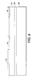
- Fig. 1 is a cross-sectional view of a silicon-on-insulator wafer used to fabricate, according to an exemplary embodiment of the invention, a device comprising a plurality of heterogeneous devices;
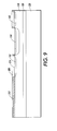
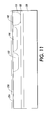
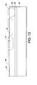
- Figs. 2-32 are cross-sectional views illustrating an exemplary method of fabricating, according to the invention, a device comprising a plurality of heterogeneous devices.
- a heterogeneous device comprises a substrate and a plurality of heterogeneous circuit devices defined in the substrate.
- the heterogeneous device may further comprise at least one microelectromechanical system-based element and/or at least one photodiode.
- the heterogeneous circuit devices may comprise a CMOS transistor and a DMOS transistor.
- the overall size of a given component is reduced. Further, since separate chip are not bonded together to form the heterogeneous device, potential problems with accuracy and noises are reduced or even eliminated. Costs are further reduced by eliminating the need for separate processes for each of the different circuit devices and eliminating the combining process.
- integrated-circuit-based manufacturing techniques are used to fabricate the heterogeneous devices and this integration can be extended to include surface and/or bulk micromachined devices on the same substrate.
- Such manufacturing technologies are relatively advanced compared to other potential technologies, yielding more reliable results and greater flexibility.
- Figs. 1-32 illustrate various steps of an exemplary embodiment of a method according to this invention. It should be understood that conventional processing techniques, such as prefurnace cleaning, and details that would be apparent to one of ordinary skill in the art, such as the use of monitor wafers, are omitted from the description of the exemplary embodiment for the sake of brevity. Also, unless important to this invention, specific details such as furnace treatments and etching times are omitted since various parameters may be employed without departing from this invention. Unless otherwise specified, the details provided are approximate ranges and reasonable modifications are contemplated.
- the process of the exemplary embodiment begins with a silicon-on-insulator (SOI) wafer 100, although the same embodiment can be implemented on a bulk silicon substrate as well.
- the silicon-on-insulator wafer 100 comprises a single-crystal-silicon (SCS) layer 110, a silicon substrate 120 and an insulator layer 130 therebetween.
- the single-crystal-silicon (SCS) layer 110 may be, for example, 5 microns thick.
- the single-crystal-silicon (SCS) layer 110 and the silicon substrate 120 may be doped, for example with boron, to form p-type silicon, depending on the desired heterogeneous device.
- the exemplary fabrication process provides a CMOS transistor 140, a DMOS transistor 150, a photodiode 160 and a microelectromechanical system-based element 160 in the single-crystal-silicon (SCS) layer 110.
- a first protective layer 212 of greater than about 7000 angstroms is formed over the single-crystal-silicon layer 110.
- the first protective layer 212 may be an oxide, either grown in a wet steam or in a dry oxygen ambient.
- any suitable process either known or hereafter developed, may be used to form a protective layer and any suitable material, either known or hereafter developed, such as, for example, silicon nitride, may be used for a protective layer.
- a first mask 201 is formed over the first protective layer 212.
- the first mask 201 may be, for example, a photoresist that is formed by any suitable photolithography process, either known or hereafter developed.
- a portion of the first protective layer 212 is removed, for example, by etching. Any suitable wet or dry etching technique, either known or hereafter developed, may be used.
- any suitable etchant such as a hydrofluoric acid etchant, may be used for the given material of the first protective layer 212.
- a high voltage n-well 152 of the DMOS transistor 150 is ion implanted in the single-crystal-silicon layer 110.
- the ion implantation of the high voltage n-well 152 may be accomplished using any suitable implantation technique, either known or hereafter developed.
- the first mask 201 is then removed or stripped using any suitable method, either known or hereafter developed.
- a second mask 202 is formed over the first protective layer 212 and the high voltage n-well 152. Using the second mask 202, a portion of the first protective layer 212 is removed, for example, by etching. As described below, the second mask 202 also serves as a protective layer for the high voltage n-well 152 during ion implantation for the CMOS transistor 140.
- a low voltage n-well 142 of the CMOS transistor 140 is ion implanted in the single-crystal-silicon layer 110. As shown in Fig. 6, the second mask 202 is then removed.
- a thin layer of thermal oxide 214 is grown on the opening windows for high-voltage and low-voltage n-wells 152 and 142. This oxidation will create a step height difference between the n-well areas and the rest of the single-crystal-silicon layer 110 which is useful for alignment purpose in the subsequent processing steps.
- the thickness of oxide 214 can range from about 1500 angstroms to about 3000 angstroms.
- a third mask 203 is formed over the protective oxide layers 214 and 212. Using the third mask 203, a portion of the first protective layer 212 is removed, for example, by etching.
- a low voltage p-well 144 of the CMOS transistor 140 is ion implanted in the single-crystal-silicon layer 110. As shown in Fig. 10, the third mask 203 is then removed.
- a diffusion process may be used to drive in the p-well 144 and the n-wells 142 and 152. Then, the fist protective layer 212 along with the second protective layer 214 is removed.
- a local oxidation of silicon (LOCOS) process may be used.
- LOC local oxidation of silicon
- a pad oxide 216 is formed over the single-crystal-silicon layer 110, the p-well 144 and the n-wells 142 and 152, as shown in Fig. 11.
- the pad oxide 216 should have a thickness in the range of about 300 angstroms to about 700 angstroms. In particular, the pad oxide 216 may have a thickness of about 500 angstroms.
- the pad oxide 216 should be grown in a temperature in a range of about 850-1000 degrees Celsius. In particular, the temperature may be about 900 degrees Celsius.
- a nitride layer 218 is deposited over the pad oxide 216.
- the nitride layer 218 may be deposited using any suitable technique, either known or hereafter developed, such as low pressure chemical vapor deposition (LPCVD).
- LPCVD low pressure chemical vapor deposition
- the nitride layer 218 should have a thickness in the range of about 1000 angstroms to about 1400 angstroms. In particular, the nitride layer 218 may have a thickness of about 1200 angstroms.
- the nitride layer 218 should be deposited in a temperature in a range of about 450-900 degrees Celsius. In particular, the temperature may be about 820 degrees Celsius.
- a fourth mask 204 is formed over the nitride layer 218.
- a portion of the nitride layer 218 is removed, for example, by etching.
- a reactive ion etch (RIE) is used to achieve a better dimension control on transistor devices.
- RIE reactive ion etch
- the structure is subjected to a field oxidation to form a field oxide layer 180.
- the field oxide layer 180 should have a thickness greater than about 1.15 microns.
- the field oxide layer 180 should be grown in a temperature in a range of about 950-1100 degrees Celsius. In particular, the temperature may be about 1000 degrees Celsius.
- the nitride layer 218 is removed, along with any oxide that may be on the nitride layer 218, using one or more wet etches. Then, as shown in Fig. 16, the pad oxide 216 is removed using a wet etch. A dry etch may damage (because of ion bombardment) active region of transistors and deteriorate transistor performance.
- a sacrificial oxide layer is provided as a protective layer for a blanket implantation (no mask) for threshold adjustment.
- the sacrificial oxide layer is stripped after the blanket implantation.
- a high quality gate oxide layer 182 is formed over the single-crystal-silicon layer 110 and the field oxide 180.
- the gate oxide layer 182 should have a thickness in a range of about 300 angstroms to about 400 angstroms. In particular, the gate oxide layer 182 may have a thickness of about 350 angstroms. Also, the gate oxide layer 182 should be grown in a temperature in a range of about 900-1000 degrees Celsius. In particular, the temperature may be about 950 degrees Celsius.
- a polysilicon layer 184 is formed over the field oxide layer 180 and the gate oxide layer 182.
- the polysilicon layer 184 may be deposited using any suitable technique, such as chemical vapor deposition (CVD).
- the polysilicon layer 184 should have a thickness in a range of about 5000 angstroms to about 8000 angstroms. In particular, the polysilicon layer 184 may have a thickness of about 6000 angstroms.
- the polysilicon layer 184 is doped with a suitable n-type dopant, such as arsenic or phosphorus. A partial wet etch of surface oxide, known as deglazing, is then carried out.
- a fifth mask 205 is formed over the polysilicon layer 184.
- a portion of the polysilicon layer 184 is removed, for example, by etching, to obtain polysilicon gates and electrical interconnects for each of the high voltage n-well 152, the low voltage n-well 142 and the low voltage p-well 144.
- a reactive ion etch (RIE) should be used to avoid etching the gate oxide 182.
- the fifth mask 205 is removed.
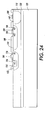
- a sixth mask 206 is formed over the field oxide layer 180 the polysilicon gates 184.
- a P-body 154 is ion implanted in the high voltage n-well 152 of the DMOS transistor 150.
- the sixth mask 206 is removed.
- a high temperature process in inert gas is then applied to drive in the P-body 154.
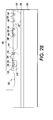
- a seventh mask 207 is formed over the field oxide layer 180 the polysilicon gates 184.
- an N+ source/drain 156 is ion implanted in each of the P-body 154 and the high voltage n-well 152 of the DMOS transistor 150, and an N+ source/drain 146 is ion implanted in the low voltage p-well 144 of the CMOS transistor 140.
- the seventh mask 207 is removed.
- an eighth mask 208 is formed over the field oxide layer 180 the polysilicon gates 184.
- a P+ source/drain 158 is ion implanted in the P-body 154 of the DMOS transistor 150 and a P+ source/drain 148 is ion implanted in the low voltage n-well 144 of the CMOS transistor 140.
- the eighth mask 208 is removed.
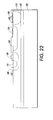
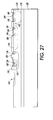
- a desired p-n junction may be ion implanted in the single-crystal-silicon layer 110 to create the photodiode 160, as shown in Fig. 27.
- forming the photodiode 160 may include steps of ion implantation, annealing, and deposition of dielectrics.
- a passivation oxide layer 186 is formed over the CMOS transistor 140, the DMOS transistor 150 and the photodiode 160, as shown in Fig. 28.
- the passivation oxide layer 186 may be formed using any suitable technique, such as plasma enhanced chemical vapor deposition (PECVD).
- PECVD plasma enhanced chemical vapor deposition
- the passivation oxide layer 186 should have a thickness of greater than about 4500 angstroms. In particular, the passivation oxide layer 186 may have a thickness of about 5000 angstroms.
- the passivation oxide layer 186 is annealed in an inert gas, for example, at about 900 degrees Celsius.
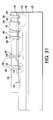
- a ninth mask 209 is formed over the passivation oxide layer 186.
- a plurality of vias 220 are formed through the passivation oxide layer 186 to the N+ and P+ sources/drains 146, 156 and 148, 158.
- Any suitable technique may be used to form the vias 220, such as a reactive ion etch (RIE) and/or a hydrofluoric acid etch.
- RIE reactive ion etch
- the ninth mask 209 is then removed.
- a metal layer 188 for example, aluminum, is formed over the passivation oxide layer 186 and in the vias 220.
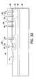
- the metal layer may be formed by any suitable technique, either known or hereafter developed, such as sputtering. As shown in Fig. 31, the metal layer 188 is partially removed using a tenth mask (not shown) and any suitable technique, such as etching. The tenth mask is removed by any suitable stripping technique.
- Any suitable approach for improving metal-semiconductor contacts may be employed.
- a pre-alloy cleaning in hot acetone and isopropyl alcohol followed by a sintering step may be used.
- any suitable techniques for forming electrical, mechanical, electromechanical or other elements of microelectromechanical system-based devices may be used to define the at least one microelectromechanical system-based element 170.
- the element 170 may be a movable mechanical element that is photolithographically defined and then released via a release etch to obtain the heterogeneous device shown in Fig. 32.
- the design and configuration of the device are illustrative and not limiting.
- the methods of this invention may be used to fabricate various devices in which heterogeneous devices are combined.
- the methods of this invention may be used to fabricate various micro-optoelectromechanical (MOEM) devices for telecommunications and other applications.
- MOEM micro-optoelectromechanical
Landscapes
- Engineering & Computer Science (AREA)
- Manufacturing & Machinery (AREA)
- Microelectronics & Electronic Packaging (AREA)
- Metal-Oxide And Bipolar Metal-Oxide Semiconductor Integrated Circuits (AREA)
- Element Separation (AREA)
- Thin Film Transistor (AREA)
- Solid State Image Pick-Up Elements (AREA)
Applications Claiming Priority (2)
| Application Number | Priority Date | Filing Date | Title |
|---|---|---|---|
| US09/683,857 US6861341B2 (en) | 2002-02-22 | 2002-02-22 | Systems and methods for integration of heterogeneous circuit devices |
| US683857 | 2002-02-22 |
Publications (2)
| Publication Number | Publication Date |
|---|---|
| EP1339101A2 true EP1339101A2 (fr) | 2003-08-27 |
| EP1339101A3 EP1339101A3 (fr) | 2005-11-30 |
Family
ID=27663578
Family Applications (1)
| Application Number | Title | Priority Date | Filing Date |
|---|---|---|---|
| EP03003955A Withdrawn EP1339101A3 (fr) | 2002-02-22 | 2003-02-21 | Systèmes et procédés pour l'intégration de dispositifs circuits hétérogènes |
Country Status (3)
| Country | Link |
|---|---|
| US (3) | US6861341B2 (fr) |
| EP (1) | EP1339101A3 (fr) |
| JP (1) | JP2003297948A (fr) |
Cited By (2)
| Publication number | Priority date | Publication date | Assignee | Title |
|---|---|---|---|---|
| GB2442253A (en) * | 2006-09-13 | 2008-04-02 | X Fab Uk Ltd | A Semiconductor device |
| US8869390B2 (en) | 2007-10-01 | 2014-10-28 | Innurvation, Inc. | System and method for manufacturing a swallowable sensor device |
Families Citing this family (15)
| Publication number | Priority date | Publication date | Assignee | Title |
|---|---|---|---|---|
| US6861341B2 (en) * | 2002-02-22 | 2005-03-01 | Xerox Corporation | Systems and methods for integration of heterogeneous circuit devices |
| US6531331B1 (en) * | 2002-07-16 | 2003-03-11 | Sandia Corporation | Monolithic integration of a MOSFET with a MEMS device |
| JP4437388B2 (ja) * | 2003-02-06 | 2010-03-24 | 株式会社リコー | 半導体装置 |
| DE10343681B4 (de) | 2003-09-18 | 2007-08-09 | Atmel Germany Gmbh | Halbleiterstruktur und deren Verwendung, insbesondere zum Begrenzen von Überspannungen |
| US7058247B2 (en) * | 2003-12-17 | 2006-06-06 | International Business Machines Corporation | Silicon carrier for optical interconnect modules |
| KR100614806B1 (ko) * | 2004-10-27 | 2006-08-22 | 삼성전자주식회사 | 고내압 트랜지스터 및 이의 제조 방법 |
| JP2006123110A (ja) * | 2004-10-29 | 2006-05-18 | Foundation For The Promotion Of Industrial Science | 静電マイクロアクチュエータ、静電マイクロアクチュエータ装置、及び静電マイクロアクチュエータの駆動方法 |
| US7473579B2 (en) * | 2005-01-31 | 2009-01-06 | Purdue Research Foundation | Self-aligned wafer level integration system |
| JP2006253316A (ja) * | 2005-03-09 | 2006-09-21 | Sony Corp | 固体撮像装置 |
| US7525151B2 (en) * | 2006-01-05 | 2009-04-28 | International Rectifier Corporation | Vertical DMOS device in integrated circuit |
| US20100117153A1 (en) * | 2008-11-07 | 2010-05-13 | Honeywell International Inc. | High voltage soi cmos device and method of manufacture |
| US8897470B2 (en) * | 2009-07-31 | 2014-11-25 | Macronix International Co., Ltd. | Method of fabricating integrated semiconductor device with MOS, NPN BJT, LDMOS, pre-amplifier and MEMS unit |
| US8377772B2 (en) * | 2010-08-17 | 2013-02-19 | Texas Instruments Incorporated | CMOS integration method for optimal IO transistor VT |
| US10094988B2 (en) | 2012-08-31 | 2018-10-09 | Micron Technology, Inc. | Method of forming photonics structures |
| US9412736B2 (en) | 2014-06-05 | 2016-08-09 | Globalfoundries Inc. | Embedding semiconductor devices in silicon-on-insulator wafers connected using through silicon vias |
Citations (3)
| Publication number | Priority date | Publication date | Assignee | Title |
|---|---|---|---|---|
| US5847280A (en) * | 1990-08-17 | 1998-12-08 | Analog Devices, Inc. | Monolithic micromechanical apparatus with suspended microstructure |
| WO1998057529A1 (fr) * | 1997-06-13 | 1998-12-17 | The Regents Of The University Of California | Dispositif microfabrique a rapport dimensionnel eleve avec isolation et interconnexions electriques |
| US5963788A (en) * | 1995-09-06 | 1999-10-05 | Sandia Corporation | Method for integrating microelectromechanical devices with electronic circuitry |
Family Cites Families (38)
| Publication number | Priority date | Publication date | Assignee | Title |
|---|---|---|---|---|
| US3207510A (en) * | 1963-03-27 | 1965-09-21 | Frederick M Gibson | Ski training device |
| US4697332A (en) * | 1984-05-25 | 1987-10-06 | Gould Inc. | Method of making tri-well CMOS by self-aligned process |
| JP3190057B2 (ja) * | 1990-07-02 | 2001-07-16 | 株式会社東芝 | 複合集積回路装置 |
| JPH05206146A (ja) | 1992-01-24 | 1993-08-13 | Toshiba Corp | 半導体装置の製造方法 |
| US5242841A (en) * | 1992-03-25 | 1993-09-07 | Texas Instruments Incorporated | Method of making LDMOS transistor with self-aligned source/backgate and photo-aligned gate |
| SE470116B (sv) * | 1992-04-03 | 1993-11-08 | Asea Brown Boveri | Detektorkrets med en som detektor arbetande halvledardiod och en med dioden integrerad förstärkarkrets |
| US5360987A (en) * | 1993-11-17 | 1994-11-01 | At&T Bell Laboratories | Semiconductor photodiode device with isolation region |
| US5498554A (en) * | 1994-04-08 | 1996-03-12 | Texas Instruments Incorporated | Method of making extended drain resurf lateral DMOS devices |
| JP3290827B2 (ja) * | 1994-09-01 | 2002-06-10 | 東芝マイクロエレクトロニクス株式会社 | 半導体装置とその製造方法 |
| JP3681794B2 (ja) * | 1995-08-30 | 2005-08-10 | 富士通株式会社 | 半導体装置の製造方法 |
| JP2816824B2 (ja) * | 1995-09-11 | 1998-10-27 | エルジイ・セミコン・カンパニイ・リミテッド | Ccd固体撮像素子 |
| US5708287A (en) * | 1995-11-29 | 1998-01-13 | Kabushiki Kaisha Toshiba | Power semiconductor device having an active layer |
| JP3575908B2 (ja) * | 1996-03-28 | 2004-10-13 | 株式会社東芝 | 半導体装置 |
| KR100220252B1 (ko) * | 1996-12-28 | 1999-09-15 | 김영환 | 반도체 소자의 제조방법 |
| US6111305A (en) * | 1997-10-09 | 2000-08-29 | Nippon Telegraph And Telephone Corporation | P-I-N semiconductor photodetector |
| US6444487B1 (en) * | 1998-07-28 | 2002-09-03 | Rosemount Aerospace Inc. | Flexible silicon strain gage |
| EP1005079B1 (fr) * | 1998-11-26 | 2012-12-26 | STMicroelectronics Srl | Procédé d'intégration d'une mémoire non volatile et d'un circuit logique à haute performance sur la même puce |
| US6214674B1 (en) * | 1998-12-02 | 2001-04-10 | United Microelectronics Corp. | Method of fabricating high voltage device suitable for low voltage device |
| US6331873B1 (en) * | 1998-12-03 | 2001-12-18 | Massachusetts Institute Of Technology | High-precision blooming control structure formation for an image sensor |
| US6207510B1 (en) * | 1999-01-12 | 2001-03-27 | Lucent Technologies Inc. | Method for making an integrated circuit including high and low voltage transistors |
| IT1306973B1 (it) * | 1999-01-12 | 2001-10-11 | St Microelectronics Srl | Procedimento per la realizzazione di strutture di isolamento percircuiti integrati. |
| IT1309087B1 (it) * | 1999-03-29 | 2002-01-16 | Olivetti Lexikon Spa | Metodo di allineamento per testine multiple di stampa a colori a gettodi inchiostro con rilevatore di posizione optoelettronico integrato. |
| US6127213A (en) * | 1999-04-14 | 2000-10-03 | United Microelectronics Corp. | Method for simultaneously forming low voltage and high voltage devices |
| US6696707B2 (en) * | 1999-04-23 | 2004-02-24 | Ccp. Clare Corporation | High voltage integrated switching devices on a bonded and trenched silicon substrate |
| US6268250B1 (en) * | 1999-05-14 | 2001-07-31 | Micron Technology, Inc. | Efficient fabrication process for dual well type structures |
| EP1067600B1 (fr) * | 1999-07-06 | 2006-11-02 | ELMOS Semiconductor AG | Procédé pour SOI compatible avec technologie CMOS |
| US6369426B2 (en) * | 2000-04-27 | 2002-04-09 | Infineon Technologies North America Corp. | Transistor with integrated photodetector for conductivity modulation |
| JP4710147B2 (ja) * | 2000-06-13 | 2011-06-29 | 株式会社デンソー | 半導体圧力センサ |
| US6580138B1 (en) * | 2000-08-01 | 2003-06-17 | Hrl Laboratories, Llc | Single crystal, dual wafer, tunneling sensor or switch with silicon on insulator substrate and a method of making same |
| WO2002012116A2 (fr) * | 2000-08-03 | 2002-02-14 | Analog Devices, Inc. | Procede de fabrication de systemes microelectromecaniques optiques a plaquette liee |
| SE519382C2 (sv) * | 2000-11-03 | 2003-02-25 | Ericsson Telefon Ab L M | Integrering av självinriktade MOS-högspänningskomponenter samt halvledarstruktur innefattande sådana |
| US6546798B1 (en) * | 2001-03-14 | 2003-04-15 | The United States Of America As Represented By The Secretary Of The Navy | Micro-electro-mechanical systems resonant optical gyroscope |
| US6861341B2 (en) * | 2002-02-22 | 2005-03-01 | Xerox Corporation | Systems and methods for integration of heterogeneous circuit devices |
| US6946371B2 (en) * | 2002-06-10 | 2005-09-20 | Amberwave Systems Corporation | Methods of fabricating semiconductor structures having epitaxially grown source and drain elements |
| US6642076B1 (en) * | 2002-10-22 | 2003-11-04 | Taiwan Semiconductor Manufacturing Company | Asymmetrical reset transistor with double-diffused source for CMOS image sensor |
| US6750489B1 (en) * | 2002-10-25 | 2004-06-15 | Foveon, Inc. | Isolated high voltage PMOS transistor |
| US20040157426A1 (en) * | 2003-02-07 | 2004-08-12 | Luc Ouellet | Fabrication of advanced silicon-based MEMS devices |
| JP2006134951A (ja) * | 2004-11-02 | 2006-05-25 | Matsushita Electric Ind Co Ltd | 固体撮像装置 |
-
2002
- 2002-02-22 US US09/683,857 patent/US6861341B2/en not_active Expired - Fee Related
-
2003
- 2003-02-21 EP EP03003955A patent/EP1339101A3/fr not_active Withdrawn
- 2003-02-21 JP JP2003044067A patent/JP2003297948A/ja active Pending
- 2003-12-04 US US10/727,692 patent/US7352047B2/en not_active Expired - Fee Related
-
2004
- 2004-11-17 US US10/990,711 patent/US7341930B2/en not_active Expired - Fee Related
Patent Citations (3)
| Publication number | Priority date | Publication date | Assignee | Title |
|---|---|---|---|---|
| US5847280A (en) * | 1990-08-17 | 1998-12-08 | Analog Devices, Inc. | Monolithic micromechanical apparatus with suspended microstructure |
| US5963788A (en) * | 1995-09-06 | 1999-10-05 | Sandia Corporation | Method for integrating microelectromechanical devices with electronic circuitry |
| WO1998057529A1 (fr) * | 1997-06-13 | 1998-12-17 | The Regents Of The University Of California | Dispositif microfabrique a rapport dimensionnel eleve avec isolation et interconnexions electriques |
Cited By (5)
| Publication number | Priority date | Publication date | Assignee | Title |
|---|---|---|---|---|
| GB2442253A (en) * | 2006-09-13 | 2008-04-02 | X Fab Uk Ltd | A Semiconductor device |
| WO2008065441A1 (fr) * | 2006-09-13 | 2008-06-05 | X-Fab Semiconductor Foundries Ag | Dispositif semi-conducteur |
| US8120121B2 (en) | 2006-09-13 | 2012-02-21 | X-Fab Semiconductor Foundries Ag | Semiconductor device |
| US8869390B2 (en) | 2007-10-01 | 2014-10-28 | Innurvation, Inc. | System and method for manufacturing a swallowable sensor device |
| US9730336B2 (en) | 2007-10-01 | 2017-08-08 | Innurvation, Inc. | System for manufacturing a swallowable sensor device |
Also Published As
| Publication number | Publication date |
|---|---|
| US20050095790A1 (en) | 2005-05-05 |
| US7341930B2 (en) | 2008-03-11 |
| JP2003297948A (ja) | 2003-10-17 |
| US20030162375A1 (en) | 2003-08-28 |
| EP1339101A3 (fr) | 2005-11-30 |
| US7352047B2 (en) | 2008-04-01 |
| US20040084745A1 (en) | 2004-05-06 |
| US6861341B2 (en) | 2005-03-01 |
Similar Documents
| Publication | Publication Date | Title |
|---|---|---|
| US6861341B2 (en) | Systems and methods for integration of heterogeneous circuit devices | |
| US10446643B2 (en) | Sealed cavity structures with a planar surface | |
| US6531331B1 (en) | Monolithic integration of a MOSFET with a MEMS device | |
| CN101292334B (zh) | 源极区和漏极区之间具有box层的应变硅mos器件 | |
| US6512258B2 (en) | Semiconductor device and method of manufacturing same | |
| US5047358A (en) | Process for forming high and low voltage CMOS transistors on a single integrated circuit chip | |
| US7691663B2 (en) | CMOS image sensor having double gate insulator therein and method for manufacturing the same | |
| US5294823A (en) | SOI BICMOS process | |
| TWI468334B (zh) | 積體半導體元件之製造方法及其結構 | |
| CN101154613A (zh) | 集成电路的形成方法 | |
| EP0356202B1 (fr) | Transistor à effet de champ MOS et procédé pour sa fabrication | |
| US5319235A (en) | Monolithic IC formed of a CCD, CMOS and a bipolar element | |
| US7847401B2 (en) | Methods, systems and structures for forming semiconductor structures incorporating high-temperature processing steps | |
| KR100407538B1 (ko) | SiGe BiCMOS 집적 설계에 의한 폴리-폴리 캐패시터의제조방법 | |
| US7312129B2 (en) | Method for producing two gates controlling the same channel | |
| US7348233B1 (en) | Methods for fabricating a CMOS device including silicide contacts | |
| US5631177A (en) | Process for manufacturing integrated circuit with power field effect transistors | |
| US5474944A (en) | Process for manufacturing integrated circuit with power field effect transistors | |
| EP0622850A1 (fr) | Diode de protection contre des décharges électrostatiques pour une technologie silicium-sur-isolant | |
| US6046078A (en) | Semiconductor device fabrication with reduced masking steps | |
| JPH06291262A (ja) | 半導体装置の製造方法 | |
| US7772653B1 (en) | Semiconductor apparatus comprising bipolar transistors and metal oxide semiconductor transistors | |
| WO1997049131A1 (fr) | Dispositif semi-conducteur comportant une couche conductrice de siliciure enterree | |
| JPH06163842A (ja) | 半導体集積回路装置及びその製造方法 | |
| SE517452C2 (sv) | Metalloxidhalvledaranordning och förfarande för dess tillverkning |
Legal Events
| Date | Code | Title | Description |
|---|---|---|---|
| PUAI | Public reference made under article 153(3) epc to a published international application that has entered the european phase |
Free format text: ORIGINAL CODE: 0009012 |
|
| AK | Designated contracting states |
Designated state(s): AT BE BG CH CY CZ DE DK EE ES FI FR GB GR HU IE IT LI LU MC NL PT SE SI SK TR |
|
| AX | Request for extension of the european patent |
Extension state: AL LT LV MK RO |
|
| PUAL | Search report despatched |
Free format text: ORIGINAL CODE: 0009013 |
|
| AK | Designated contracting states |
Kind code of ref document: A3 Designated state(s): AT BE BG CH CY CZ DE DK EE ES FI FR GB GR HU IE IT LI LU MC NL PT SE SI SK TR |
|
| AX | Request for extension of the european patent |
Extension state: AL LT LV MK RO |
|
| 17P | Request for examination filed |
Effective date: 20060530 |
|
| AKX | Designation fees paid |
Designated state(s): DE FR GB |
|
| 17Q | First examination report despatched |
Effective date: 20060726 |
|
| STAA | Information on the status of an ep patent application or granted ep patent |
Free format text: STATUS: THE APPLICATION IS DEEMED TO BE WITHDRAWN |
|
| 18D | Application deemed to be withdrawn |
Effective date: 20091027 |