EP1341217A2 - Condensateur pour un dispositif semiconducteur, sa méthode de fabrication et dispositif électronique le comprenant - Google Patents
Condensateur pour un dispositif semiconducteur, sa méthode de fabrication et dispositif électronique le comprenant Download PDFInfo
- Publication number
- EP1341217A2 EP1341217A2 EP02257345A EP02257345A EP1341217A2 EP 1341217 A2 EP1341217 A2 EP 1341217A2 EP 02257345 A EP02257345 A EP 02257345A EP 02257345 A EP02257345 A EP 02257345A EP 1341217 A2 EP1341217 A2 EP 1341217A2
- Authority
- EP
- European Patent Office
- Prior art keywords
- dielectric layer
- capacitor
- thin dielectric
- precursor
- buffer layer
- Prior art date
- Legal status (The legal status is an assumption and is not a legal conclusion. Google has not performed a legal analysis and makes no representation as to the accuracy of the status listed.)
- Ceased
Links
Images



Classifications
-
- H—ELECTRICITY
- H10—SEMICONDUCTOR DEVICES; ELECTRIC SOLID-STATE DEVICES NOT OTHERWISE PROVIDED FOR
- H10D—INORGANIC ELECTRIC SEMICONDUCTOR DEVICES
- H10D84/00—Integrated devices formed in or on semiconductor substrates that comprise only semiconducting layers, e.g. on Si wafers or on GaAs-on-Si wafers
-
- H—ELECTRICITY
- H10—SEMICONDUCTOR DEVICES; ELECTRIC SOLID-STATE DEVICES NOT OTHERWISE PROVIDED FOR
- H10D—INORGANIC ELECTRIC SEMICONDUCTOR DEVICES
- H10D1/00—Resistors, capacitors or inductors
- H10D1/60—Capacitors
- H10D1/68—Capacitors having no potential barriers
- H10D1/682—Capacitors having no potential barriers having dielectrics comprising perovskite structures
- H10D1/684—Capacitors having no potential barriers having dielectrics comprising perovskite structures the dielectrics comprising multiple layers, e.g. comprising buffer layers, seed layers or gradient layers
-
- H—ELECTRICITY
- H10—SEMICONDUCTOR DEVICES; ELECTRIC SOLID-STATE DEVICES NOT OTHERWISE PROVIDED FOR
- H10D—INORGANIC ELECTRIC SEMICONDUCTOR DEVICES
- H10D1/00—Resistors, capacitors or inductors
- H10D1/60—Capacitors
- H10D1/68—Capacitors having no potential barriers
- H10D1/682—Capacitors having no potential barriers having dielectrics comprising perovskite structures
-
- H—ELECTRICITY
- H10—SEMICONDUCTOR DEVICES; ELECTRIC SOLID-STATE DEVICES NOT OTHERWISE PROVIDED FOR
- H10D—INORGANIC ELECTRIC SEMICONDUCTOR DEVICES
- H10D1/00—Resistors, capacitors or inductors
- H10D1/60—Capacitors
- H10D1/68—Capacitors having no potential barriers
- H10D1/692—Electrodes
- H10D1/694—Electrodes comprising noble metals or noble metal oxides
-
- H—ELECTRICITY
- H10—SEMICONDUCTOR DEVICES; ELECTRIC SOLID-STATE DEVICES NOT OTHERWISE PROVIDED FOR
- H10D—INORGANIC ELECTRIC SEMICONDUCTOR DEVICES
- H10D84/00—Integrated devices formed in or on semiconductor substrates that comprise only semiconducting layers, e.g. on Si wafers or on GaAs-on-Si wafers
- H10D84/80—Integrated devices formed in or on semiconductor substrates that comprise only semiconducting layers, e.g. on Si wafers or on GaAs-on-Si wafers characterised by the integration of at least one component covered by groups H10D12/00 or H10D30/00, e.g. integration of IGFETs
- H10D84/811—Combinations of field-effect devices and one or more diodes, capacitors or resistors
-
- H—ELECTRICITY
- H10—SEMICONDUCTOR DEVICES; ELECTRIC SOLID-STATE DEVICES NOT OTHERWISE PROVIDED FOR
- H10D—INORGANIC ELECTRIC SEMICONDUCTOR DEVICES
- H10D84/00—Integrated devices formed in or on semiconductor substrates that comprise only semiconducting layers, e.g. on Si wafers or on GaAs-on-Si wafers
- H10D84/80—Integrated devices formed in or on semiconductor substrates that comprise only semiconducting layers, e.g. on Si wafers or on GaAs-on-Si wafers characterised by the integration of at least one component covered by groups H10D12/00 or H10D30/00, e.g. integration of IGFETs
- H10D84/811—Combinations of field-effect devices and one or more diodes, capacitors or resistors
- H10D84/813—Combinations of field-effect devices and capacitor only
-
- H—ELECTRICITY
- H10—SEMICONDUCTOR DEVICES; ELECTRIC SOLID-STATE DEVICES NOT OTHERWISE PROVIDED FOR
- H10P—GENERIC PROCESSES OR APPARATUS FOR THE MANUFACTURE OR TREATMENT OF DEVICES COVERED BY CLASS H10
- H10P14/00—Formation of materials, e.g. in the shape of layers or pillars
- H10P14/60—Formation of materials, e.g. in the shape of layers or pillars of insulating materials
- H10P14/65—Formation of materials, e.g. in the shape of layers or pillars of insulating materials characterised by treatments performed before or after the formation of the materials
- H10P14/6502—Formation of materials, e.g. in the shape of layers or pillars of insulating materials characterised by treatments performed before or after the formation of the materials of treatments performed before formation of the materials
- H10P14/6506—Formation of intermediate materials
-
- H—ELECTRICITY
- H10—SEMICONDUCTOR DEVICES; ELECTRIC SOLID-STATE DEVICES NOT OTHERWISE PROVIDED FOR
- H10P—GENERIC PROCESSES OR APPARATUS FOR THE MANUFACTURE OR TREATMENT OF DEVICES COVERED BY CLASS H10
- H10P14/00—Formation of materials, e.g. in the shape of layers or pillars
- H10P14/60—Formation of materials, e.g. in the shape of layers or pillars of insulating materials
- H10P14/69—Inorganic materials
- H10P14/692—Inorganic materials composed of oxides, glassy oxides or oxide-based glasses
- H10P14/6938—Inorganic materials composed of oxides, glassy oxides or oxide-based glasses the material containing at least one metal element, e.g. metal oxides, metal oxynitrides or metal oxycarbides
- H10P14/6939—Inorganic materials composed of oxides, glassy oxides or oxide-based glasses the material containing at least one metal element, e.g. metal oxides, metal oxynitrides or metal oxycarbides characterised by the metal
- H10P14/69394—Inorganic materials composed of oxides, glassy oxides or oxide-based glasses the material containing at least one metal element, e.g. metal oxides, metal oxynitrides or metal oxycarbides characterised by the metal the material containing titanium, e.g. TiO2
-
- H—ELECTRICITY
- H10—SEMICONDUCTOR DEVICES; ELECTRIC SOLID-STATE DEVICES NOT OTHERWISE PROVIDED FOR
- H10P—GENERIC PROCESSES OR APPARATUS FOR THE MANUFACTURE OR TREATMENT OF DEVICES COVERED BY CLASS H10
- H10P14/00—Formation of materials, e.g. in the shape of layers or pillars
- H10P14/60—Formation of materials, e.g. in the shape of layers or pillars of insulating materials
- H10P14/69—Inorganic materials
- H10P14/692—Inorganic materials composed of oxides, glassy oxides or oxide-based glasses
- H10P14/6938—Inorganic materials composed of oxides, glassy oxides or oxide-based glasses the material containing at least one metal element, e.g. metal oxides, metal oxynitrides or metal oxycarbides
- H10P14/69398—Inorganic materials composed of oxides, glassy oxides or oxide-based glasses the material containing at least one metal element, e.g. metal oxides, metal oxynitrides or metal oxycarbides the material having a perovskite structure, e.g. BaTiO3
-
- H—ELECTRICITY
- H10—SEMICONDUCTOR DEVICES; ELECTRIC SOLID-STATE DEVICES NOT OTHERWISE PROVIDED FOR
- H10P—GENERIC PROCESSES OR APPARATUS FOR THE MANUFACTURE OR TREATMENT OF DEVICES COVERED BY CLASS H10
- H10P95/00—Generic processes or apparatus for manufacture or treatments not covered by the other groups of this subclass
-
- H—ELECTRICITY
- H10—SEMICONDUCTOR DEVICES; ELECTRIC SOLID-STATE DEVICES NOT OTHERWISE PROVIDED FOR
- H10P—GENERIC PROCESSES OR APPARATUS FOR THE MANUFACTURE OR TREATMENT OF DEVICES COVERED BY CLASS H10
- H10P14/00—Formation of materials, e.g. in the shape of layers or pillars
- H10P14/60—Formation of materials, e.g. in the shape of layers or pillars of insulating materials
- H10P14/63—Formation of materials, e.g. in the shape of layers or pillars of insulating materials characterised by the formation processes
- H10P14/6326—Deposition processes
- H10P14/6328—Deposition from the gas or vapour phase
- H10P14/6334—Deposition from the gas or vapour phase using decomposition or reaction of gaseous or vapour phase compounds, i.e. chemical vapour deposition
- H10P14/6339—Deposition from the gas or vapour phase using decomposition or reaction of gaseous or vapour phase compounds, i.e. chemical vapour deposition deposition by cyclic CVD, e.g. ALD, ALE or pulsed CVD
-
- H—ELECTRICITY
- H10—SEMICONDUCTOR DEVICES; ELECTRIC SOLID-STATE DEVICES NOT OTHERWISE PROVIDED FOR
- H10P—GENERIC PROCESSES OR APPARATUS FOR THE MANUFACTURE OR TREATMENT OF DEVICES COVERED BY CLASS H10
- H10P14/00—Formation of materials, e.g. in the shape of layers or pillars
- H10P14/60—Formation of materials, e.g. in the shape of layers or pillars of insulating materials
- H10P14/66—Formation of materials, e.g. in the shape of layers or pillars of insulating materials characterised by the type of materials
- H10P14/668—Formation of materials, e.g. in the shape of layers or pillars of insulating materials characterised by the type of materials the materials being characterised by the deposition precursor materials
Definitions
- the present invention relates to a capacitor for a semiconductor device, and more particularly, to a capacitor for use in a semiconductor device, which can effectively suppress the oxidization of a material for an electrode, when forming a thin dielectric layer, a manufacturing method thereof, and an electronic device that employs the capacitor and thus can be highly integrated.
- ALD atomic layer deposition
- a desired metal oxide thin dielectric film is obtained by chemically absorbing an organometallic compound, which is a precursor, on a substrate, and processing the thin film under an oxygen atmosphere.
- the ALD method is advantageous in that an organic substance included in a precursor can be removed by a strong oxidizer since the precursor and the oxidizer are introduced using time division.
- a lower electrode which is to be formed below a thin dielectric layer when forming an atomic layer, is formed of a material that is prone to oxidization, e.g., ruthenium (Ru), the Ru electrode may be deformed and the thin dielectric layer may deteriorate, as shown in FIG. 1. Therefore, the thin dielectric layer is difficult to highly integrate.
- ruthenium ruthenium
- FIG. 1 is a view of a capacitor in which a thin strontium titanium oxide (SrTiO 3 ) layer is formed on a Ru lower electrode by a conventional O 3 atomic layer deposition (ALD) method.
- a protrusion of the Ru lower electrode is caused in the capacitor.
- Ru easily changes into RuO 2 or RuO 4 under an oxygen atmosphere, which causes the deformation of the Ru electrode.
- a capacitor for use in a semiconductor device including upper and lower electrodes, each formed of a platinum group metal; a thin dielectric layer disposed between the upper and lower electrodes; and a buffer layer disposed between the lower electrode and the thin dielectric layer, the buffer layer including a metal oxide of Group 3, 4, or 13.
- the invention may provide a capacitor for use in a semiconductor device, in which the oxidization of a material for an electrode is effectively suppressed when forming a thin dielectric layer.
- a method of fabricating such a capacitor for use in a semiconductor device including: forming a buffer layer on a lower electrode of a platinum group metal by performing an atomic layer deposition (ALD) process using a precursor for the buffer layer; forming a thin dielectric layer by performing the ALD process using a precursor for a thin dielectric layer on the buffer layer; and forming an upper electrode of a platinum group metal on the thin dielectric layer.
- ALD atomic layer deposition
- a method of fabricating such a capacitor for use in a semiconductor device including: absorbing CO on a surface of a lower electrode of a platinum group metal; placing the lower electrode under a reducing atmosphere to produce a lattice oxygen; forming a thin dielectric layer by performing an ALD process using a precursor for the thin dielectric layer, using the lattice oxygen; and forming an upper electrode of a platinum group metal on the thin dielectric layer.
- an electronic device employing the capacitor above for a semiconductor device.
- This device may accordingly integrate a thin dielectric layer.
- a buffer layer is formed between a thin dielectric layer and an electrode so as to prevent the oxidization of a platinum metal, especially, ruthenium (Ru), which is a material for an electrode, when forming the thin dielectric film.
- the buffer layer is formed of a metal oxide of Group 3, 4, or 13, preferably, at least one selected from TiO 2 , Al 2 O 3 , Ta 2 O 5 , and HfO 2 .
- Such a buffer layer may be formed by an atomic layer deposition (ALD) of a precursor for forming the buffer layer.
- the precursor is an organometallic compound having a small sized ligand or that is easily decomposed when being absorbed on a substrate and causes the chemical absorption of a by-product. The use of such an organometallic compound allows an atomic layer of a higher packing density to be formed on an electrode.
- a metal precursor includes Ti(i-OPr) 4 or Ti(l-OPr) 2 (tmhd) 2 for TiO 2 buffer layer (tmhd indicates tetramethylheptanedionate, and i-OPr indicates isopropoxy); Al(CH 3 ) 3 or AlCl 3 for an Al 2 O 3 buffer layer; Ta(OEt) 5 (OEt indicates ethoxide) for a Ta 2 O 5 buffer layer; and HfCl 4 , Hf(OBu) 4 for an HfO 2 buffer layer.
- the surface of a Ru electrode is not directly in contact with ozone (O 3 ) or oxygen when a thin dielectric layer is formed. Further, it is possible to prevent the deformation of the electrode or the deterioration of the characteristics of a thin dielectric layer casued by the oxidization of the electrode.
- the vapor deposition temperature of the precursor for a buffer layer depends largely on the characteristics of the precursor but preferably is 200 - 500°C. This is because the reactivity between the precursor and O 3 , which is used as an oxidizer, is lowered where the deposition temperature is less than 200°C, and the precursor is decomposed so as not to form a buffer layer using ALD method if the deposition temperature is greater than 500°C.
- a lower electrode is formed of a platinum group metal. At least one element is selected, as the platinum group metal, from the group consisting of ruthenium (Ru), osmium (Os), iridium (Ir), and platinum (Pt).
- a buffer layer is formed by performing the ALD process using a precursor for a buffer layer on the lower electrode.
- a thin dielectric layer is formed by performing the ALD process using a precursor for a thin dielectric layer on the buffer layer.
- the thin dielectric layer is formed of SrTiO 3 , BaTiO 3 , Pb(Zr,Ti)O 3 , or the like.
- SrTiO 3 one of Sr(tmhd) 2 or Sr(methd) 2 (methd indicates methoxyethoxy tetramethylheptanedionate) is selected as Sr source, one of TiO(tmhd) 2 or TiO(l ⁇ OPr) 2 (tmhd) 2 is selected as Ti source, and then the selected elements are mixed together.
- the ALD process is performed using the precursor for the thin dielectric layer and oxygen gas or heat source.
- the vapor deposition temperature of an atomic layer is 300 - 500°C.
- the capacitor for use in a semiconductor device according to the present invention is completed by forming an upper electrode on the thin dielectric layer using a platinum group metal.
- a lattice oxygen obtained from carbon monoxide (CO) that is absorbed in a material for an electrode is used as an oxidation.
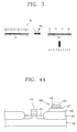
- FIG. 3 is a view explaining a process of producing lattice oxygen when a Ru electrode is adopted.
- CO absorbed on the Ru electrode is placed under a reducing atmosphere and the carbon in the CO is removed in the form of CH 4 .
- CH 4 the carbon in the CO
- CO is absorbed on the surface of a lower electrode made of an element of a platinum group metal.
- the resultant is placed under a reducing atmosphere to produce lattice oxygen.
- the temperature can be maintained at 100 - 500°C. This is because CO is difficult to reduce if the temperature is lower than 100°C, and CO is eearliestr desorbed from the surface of a lower electrode carbon if the process temperature is higher than 500°C.
- the reducing atmosphere is formed using a reducing gas such as hydrogen.
- a thin dielectric layer is formed by performing the ALD process using a precursor for a thin dielectric layer, using the lattice oxygen.
- a method of forming the thin dielectric layer and the required materials are as described above.
- a capacitor for use in a semiconductor device according to the present invention is completed by forming an upper electrode from an element of a platinum group metal on the thin dielectric layer.
- Such a capacitor can be applied to various electronic devices such as a dynamic RAM (DRAM) device and non-volatile memory (FRAM).
- DRAM dynamic RAM
- FRAM non-volatile memory
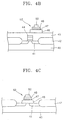
- FIGs. 4A through 4C are cross-sectional views of several forms memory devices adopting a capacitor according to the present invention. More specifically, FIG. 4A is a cross-sectional view of a memory device of a single transistor type, FIG. 4B is a cross sectional view of a 1Tr-1C type memory device, and FIG. 4C is a cross sectional view of a 1Tr-1C COB-type memory device.
- reference numerals '40' denotes a silicon substrate; '41', an active region; '42', a non-active region; '43', a lower structure; '44', a gate electrode; '45', a polysilicon layer; '46', a lower electrode; '47', a buffer layer of TiO 2 ; '48', a thin dielectric layer of SrTiO 3 ; '50', an upper electrode; and '52', a capacitor.
- FIGS. 4A through 4C various memory devices adopting a preferred embodiment of a capacitor according to the present invention are illustrated, but such a capacitor can be applied to other electronic devices having a thin dielectric layer.
- ALD atomic layer deposition
- the ALD process was performed on the buffer layer at about 400°C, using Sr(mdthd) 2 and Ti(i-OPr) 2 (tmhd) 2 as a precursor and O 3 as an oxidizer to form a thin dielectric layer of SrTiO 3 .
- a capacitor was prepared in the same manner as in the first embodiment, except that the ALD process was performed at about 400°C with Al(CH 3 ) 3 as a precursor for a buffer layer and O 3 as an oxidizer to form a buffer layer of Al 2 O 3 on a second Ru electrode.
- the laminated cross-section of a thin dielectric layer of SrTiO 3 formed on the Ru thin layer according to the first embodiment is taken by a transmission electronic microscope (TEM) as illustrated in FIG. 5.
- TEM transmission electronic microscope
- the buffer layer of TiO 2 is formed below the thin layer of SrTiO 3 , and the Ru electrode is positioned under the buffer layer of TiO 2 . It is noted that a protrusion is not formed in the Ru electrode.
- FIG. 6 is a photograph of the laminated cross-section of the thin dielectric layer of SrTiO 3 formed on the Ru thin layer according to the second embodiment, taken by a scanning electronic microscope (SEM).
- FIGs. 7A and 7B are graphs illustrating the electrical characteristics of the capacitor according to the third embodiment. More specifically, FIG. 7A shows variations in the density of electric current according to voltage. FIG. 7A reveals that 10 -7 A/cm 2 at 1V, which is the standard set for a DRAM, is generally satisfied by the capacitor prepared in the third embodiment. FIG. 7B shows variations in tox according to bias voltage.
- the 'tox' is referred to as a value that is the thickness of a thin dielectric layer calculated in the thickness of SiO 2 . The smaller the value of tox, the better the quality of a dielectric layer.
- the tox of a dielectric layer is 6.8 ⁇ just after the deposition thereof, and is 7 ⁇ , which is the tox of the dielectric layer required for a DRAM of more than 16G.
- a capacitor according to the present invention can secure the excellent electrical characteristics of a thin dielectric layer, which is required by a highly integrated memory, and therefore can be available in an electronic device such as a DRAM.
Landscapes
- Semiconductor Memories (AREA)
- Semiconductor Integrated Circuits (AREA)
- Non-Volatile Memory (AREA)
Priority Applications (1)
| Application Number | Priority Date | Filing Date | Title |
|---|---|---|---|
| EP07114231A EP1855310A3 (fr) | 2002-02-28 | 2002-10-23 | Condensateur pour dispositif à semi-conducteurs, son procédé de fabrication, et dispositif électronique l'utilisant |
Applications Claiming Priority (2)
| Application Number | Priority Date | Filing Date | Title |
|---|---|---|---|
| KR2002010982 | 2002-02-28 | ||
| KR10-2002-0010982A KR100455287B1 (ko) | 2002-02-28 | 2002-02-28 | 반도체 장치의 커패시터, 그 제조방법 및 상기 커패시터를채용하고 있는 전자 소자 |
Related Child Applications (1)
| Application Number | Title | Priority Date | Filing Date |
|---|---|---|---|
| EP07114231A Division EP1855310A3 (fr) | 2002-02-28 | 2002-10-23 | Condensateur pour dispositif à semi-conducteurs, son procédé de fabrication, et dispositif électronique l'utilisant |
Publications (2)
| Publication Number | Publication Date |
|---|---|
| EP1341217A2 true EP1341217A2 (fr) | 2003-09-03 |
| EP1341217A3 EP1341217A3 (fr) | 2004-11-10 |
Family
ID=27725829
Family Applications (2)
| Application Number | Title | Priority Date | Filing Date |
|---|---|---|---|
| EP02257345A Ceased EP1341217A3 (fr) | 2002-02-28 | 2002-10-23 | Condensateur pour un dispositif semiconducteur, sa méthode de fabrication et dispositif électronique le comprenant |
| EP07114231A Withdrawn EP1855310A3 (fr) | 2002-02-28 | 2002-10-23 | Condensateur pour dispositif à semi-conducteurs, son procédé de fabrication, et dispositif électronique l'utilisant |
Family Applications After (1)
| Application Number | Title | Priority Date | Filing Date |
|---|---|---|---|
| EP07114231A Withdrawn EP1855310A3 (fr) | 2002-02-28 | 2002-10-23 | Condensateur pour dispositif à semi-conducteurs, son procédé de fabrication, et dispositif électronique l'utilisant |
Country Status (5)
| Country | Link |
|---|---|
| US (3) | US20030160276A1 (fr) |
| EP (2) | EP1341217A3 (fr) |
| JP (1) | JP4094970B2 (fr) |
| KR (1) | KR100455287B1 (fr) |
| CN (2) | CN1292479C (fr) |
Cited By (2)
| Publication number | Priority date | Publication date | Assignee | Title |
|---|---|---|---|---|
| EP1383162A3 (fr) * | 2002-07-20 | 2004-08-25 | Samsung Electronics Co., Ltd. | Méthode de dépôt d'une couche diélectrique |
| EP2417281A4 (fr) * | 2009-04-10 | 2013-04-03 | Micron Technology Inc | Interface en oxyde de strontium et de ruthénium |
Families Citing this family (12)
| Publication number | Priority date | Publication date | Assignee | Title |
|---|---|---|---|---|
| DE10341564B4 (de) * | 2003-09-09 | 2007-11-22 | Infineon Technologies Ag | Kondensatoranordnung und Verfahren zur Herstellung derselben |
| KR100634509B1 (ko) * | 2004-08-20 | 2006-10-13 | 삼성전자주식회사 | 3차원 반도체 캐패시터 및 그 제조 방법 |
| JP4953580B2 (ja) * | 2005-03-03 | 2012-06-13 | 富士通セミコンダクター株式会社 | 半導体装置の製造方法 |
| US7521705B2 (en) | 2005-08-15 | 2009-04-21 | Micron Technology, Inc. | Reproducible resistance variable insulating memory devices having a shaped bottom electrode |
| KR100840783B1 (ko) * | 2006-08-21 | 2008-06-23 | 삼성전자주식회사 | 전구체 기화 방법 및 장치, 및 이를 이용한 유전막 형성방법 |
| US7892964B2 (en) * | 2007-02-14 | 2011-02-22 | Micron Technology, Inc. | Vapor deposition methods for forming a metal-containing layer on a substrate |
| JP6213579B2 (ja) | 2014-02-07 | 2017-10-18 | 株式会社村田製作所 | コンデンサ |
| KR101893000B1 (ko) | 2017-03-09 | 2018-08-29 | 성균관대학교 산학협력단 | Chloride계 전자방출 물질 및 이의 제조방법 |
| US10411017B2 (en) * | 2017-08-31 | 2019-09-10 | Micron Technology, Inc. | Multi-component conductive structures for semiconductor devices |
| CN111668023B (zh) * | 2020-05-13 | 2021-10-08 | 肇庆市华师大光电产业研究院 | 一种铪铝氧薄膜的制备方法及其应用 |
| CN112080732B (zh) * | 2020-07-29 | 2021-12-28 | 西安交通大学 | 一种硅集成的bt-bmz薄膜、电容器及其制造方法 |
| KR102674344B1 (ko) | 2022-10-04 | 2024-06-11 | 고려대학교 산학협력단 | 높은 일함수 산화물반도체 중간층을 이용한 낮은 누설전류 및 높은 전기용량의 커패시터 제작 방법 및 이에 의해 제조된 커패시터 |
Family Cites Families (19)
| Publication number | Priority date | Publication date | Assignee | Title |
|---|---|---|---|---|
| US6285048B1 (en) * | 1991-12-13 | 2001-09-04 | Symetrix Corporation | Barium strontium titanate integrated circuit capacitors and process for making the same |
| US5338951A (en) * | 1991-11-06 | 1994-08-16 | Ramtron International Corporation | Structure of high dielectric constant metal/dielectric/semiconductor capacitor for use as the storage capacitor in memory devices |
| JP3182889B2 (ja) | 1992-06-25 | 2001-07-03 | セイコーエプソン株式会社 | 強誘電体装置 |
| US5395522A (en) * | 1993-02-23 | 1995-03-07 | Anatel Corporation | Apparatus for removal of organic material from water |
| JPH10182291A (ja) * | 1996-12-20 | 1998-07-07 | Sharp Corp | 強誘電体薄膜の製造方法、強誘電体薄膜被覆基板及びキャパシタ |
| US6018065A (en) * | 1997-11-10 | 2000-01-25 | Advanced Technology Materials, Inc. | Method of fabricating iridium-based materials and structures on substrates, iridium source reagents therefor |
| KR19990080412A (ko) * | 1998-04-16 | 1999-11-05 | 윤종용 | 이중 유전막을 가지는 고유전율 커패시터 및 그제조방법 |
| US6509601B1 (en) * | 1998-07-31 | 2003-01-21 | Samsung Electronics Co., Ltd. | Semiconductor memory device having capacitor protection layer and method for manufacturing the same |
| KR100327328B1 (ko) * | 1998-10-13 | 2002-05-09 | 윤종용 | 부분적으로다른두께를갖는커패시터의유전막형성방버뵤 |
| JP2000349254A (ja) * | 1999-06-02 | 2000-12-15 | Sony Corp | 誘電体キャパシタおよびメモリならびにそれらの製造方法 |
| US6144069A (en) * | 1999-08-03 | 2000-11-07 | United Microelectronics Corp. | LDMOS transistor |
| US6503330B1 (en) * | 1999-12-22 | 2003-01-07 | Genus, Inc. | Apparatus and method to achieve continuous interface and ultrathin film during atomic layer deposition |
| KR100415516B1 (ko) * | 2000-06-28 | 2004-01-31 | 주식회사 하이닉스반도체 | 반도체 소자의 캐패시터 제조 방법 |
| US6777565B2 (en) * | 2000-06-29 | 2004-08-17 | Board Of Trustees, The University Of Illinois | Organometallic compounds and their use as precursors for forming films and powders of metal or metal derivatives |
| KR100663341B1 (ko) * | 2000-08-11 | 2007-01-02 | 삼성전자주식회사 | 원자층 증착 캐패시터 제조방법 및 장치 |
| US6642567B1 (en) * | 2000-08-31 | 2003-11-04 | Micron Technology, Inc. | Devices containing zirconium-platinum-containing materials and methods for preparing such materials and devices |
| US7378719B2 (en) * | 2000-12-20 | 2008-05-27 | Micron Technology, Inc. | Low leakage MIM capacitor |
| JP2002222934A (ja) * | 2001-01-29 | 2002-08-09 | Nec Corp | 半導体装置およびその製造方法 |
| KR100431740B1 (ko) * | 2001-09-14 | 2004-05-17 | 주식회사 하이닉스반도체 | 고유전막을 구비한 반도체소자 및 그 제조 방법 |
-
2002
- 2002-02-28 KR KR10-2002-0010982A patent/KR100455287B1/ko not_active Expired - Fee Related
- 2002-10-23 EP EP02257345A patent/EP1341217A3/fr not_active Ceased
- 2002-10-23 EP EP07114231A patent/EP1855310A3/fr not_active Withdrawn
- 2002-10-24 CN CNB021471622A patent/CN1292479C/zh not_active Expired - Fee Related
- 2002-10-24 CN CNA2006101531766A patent/CN101009217A/zh active Pending
-
2003
- 2003-02-24 US US10/370,625 patent/US20030160276A1/en not_active Abandoned
- 2003-02-28 JP JP2003053123A patent/JP4094970B2/ja not_active Expired - Fee Related
-
2004
- 2004-09-01 US US10/930,953 patent/US7105401B2/en not_active Expired - Fee Related
-
2006
- 2006-09-01 US US11/514,248 patent/US20060289921A1/en not_active Abandoned
Cited By (3)
| Publication number | Priority date | Publication date | Assignee | Title |
|---|---|---|---|---|
| EP1383162A3 (fr) * | 2002-07-20 | 2004-08-25 | Samsung Electronics Co., Ltd. | Méthode de dépôt d'une couche diélectrique |
| US6911402B2 (en) | 2002-07-20 | 2005-06-28 | Samsung Electronics Co., Ltd. | Deposition method of a dielectric layer |
| EP2417281A4 (fr) * | 2009-04-10 | 2013-04-03 | Micron Technology Inc | Interface en oxyde de strontium et de ruthénium |
Also Published As
| Publication number | Publication date |
|---|---|
| CN101009217A (zh) | 2007-08-01 |
| US20030160276A1 (en) | 2003-08-28 |
| EP1855310A3 (fr) | 2009-07-15 |
| KR20030071328A (ko) | 2003-09-03 |
| EP1855310A2 (fr) | 2007-11-14 |
| KR100455287B1 (ko) | 2004-11-06 |
| US20060289921A1 (en) | 2006-12-28 |
| EP1341217A3 (fr) | 2004-11-10 |
| JP4094970B2 (ja) | 2008-06-04 |
| US20050042836A1 (en) | 2005-02-24 |
| CN1441496A (zh) | 2003-09-10 |
| JP2004006678A (ja) | 2004-01-08 |
| US7105401B2 (en) | 2006-09-12 |
| CN1292479C (zh) | 2006-12-27 |
Similar Documents
| Publication | Publication Date | Title |
|---|---|---|
| KR100450681B1 (ko) | 반도체 메모리 소자의 커패시터 및 그 제조 방법 | |
| EP1368822B1 (fr) | Barrieres d'oxygene riches en rhodium | |
| US6596602B2 (en) | Method of fabricating a high dielectric constant metal oxide capacity insulator film using atomic layer CVD | |
| EP1383162B1 (fr) | Méthode de dépôt d'une couche diélectrique | |
| KR100546324B1 (ko) | Ald에 의한 금속 산화물 박막 형성 방법, 란탄 산화막 형성 방법 및 반도체 소자의 고유전막 형성 방법 | |
| KR101123433B1 (ko) | 고 유전률을 갖는 구조물을 형성하는 방법 및 고 유전률을 갖는 구조물 | |
| US9343298B2 (en) | Metal-insulator-metal capacitor and method for manufacturing thereof | |
| US6875667B2 (en) | Method for forming capacitor | |
| EP1341217A2 (fr) | Condensateur pour un dispositif semiconducteur, sa méthode de fabrication et dispositif électronique le comprenant | |
| US8092862B2 (en) | Method for forming dielectric film and method for forming capacitor in semiconductor device using the same | |
| JP2003174146A (ja) | 強誘電体キャパシタおよびその製造方法 | |
| US6417042B2 (en) | Method of manufacturing a capacitor in a semiconductor device | |
| JP4031552B2 (ja) | 半導体装置の膜形成方法 | |
| KR101116166B1 (ko) | 반도체 소자의 커패시터 및 그 제조 방법 | |
| KR20080084434A (ko) | Mⅰm 커패시터 및 이의 제조 방법 | |
| JP2004023042A (ja) | 半導体装置および半導体装置の製造方法 | |
| JP2006229231A (ja) | 非晶質誘電膜及びその製造方法 | |
| JP2005184024A (ja) | 半導体装置およびその製造方法 | |
| JP2000323678A (ja) | 半導体装置の製造方法 |
Legal Events
| Date | Code | Title | Description |
|---|---|---|---|
| PUAI | Public reference made under article 153(3) epc to a published international application that has entered the european phase |
Free format text: ORIGINAL CODE: 0009012 |
|
| AK | Designated contracting states |
Kind code of ref document: A2 Designated state(s): AT BE BG CH CY CZ DE DK EE ES FI FR GB GR IE IT LI LU MC NL PT SE SK TR |
|
| AX | Request for extension of the european patent |
Extension state: AL LT LV MK RO SI |
|
| PUAL | Search report despatched |
Free format text: ORIGINAL CODE: 0009013 |
|
| AK | Designated contracting states |
Kind code of ref document: A3 Designated state(s): AT BE BG CH CY CZ DE DK EE ES FI FR GB GR IE IT LI LU MC NL PT SE SK TR |
|
| AX | Request for extension of the european patent |
Extension state: AL LT LV MK RO SI |
|
| 17P | Request for examination filed |
Effective date: 20050223 |
|
| AKX | Designation fees paid |
Designated state(s): DE FR GB |
|
| 17Q | First examination report despatched |
Effective date: 20070327 |
|
| STAA | Information on the status of an ep patent application or granted ep patent |
Free format text: STATUS: THE APPLICATION HAS BEEN REFUSED |
|
| 18R | Application refused |
Effective date: 20090509 |