EP1343311A2 - Méthode et appareil de compensation des pixels défectueux d'un capteur à transfert de charge - Google Patents
Méthode et appareil de compensation des pixels défectueux d'un capteur à transfert de charge Download PDFInfo
- Publication number
- EP1343311A2 EP1343311A2 EP03004413A EP03004413A EP1343311A2 EP 1343311 A2 EP1343311 A2 EP 1343311A2 EP 03004413 A EP03004413 A EP 03004413A EP 03004413 A EP03004413 A EP 03004413A EP 1343311 A2 EP1343311 A2 EP 1343311A2
- Authority
- EP
- European Patent Office
- Prior art keywords
- pixel
- charge
- value
- cell
- cells
- Prior art date
- Legal status (The legal status is an assumption and is not a legal conclusion. Google has not performed a legal analysis and makes no representation as to the accuracy of the status listed.)
- Ceased
Links
- 230000002950 deficient Effects 0.000 title claims abstract description 26
- 238000000034 method Methods 0.000 title claims abstract description 22
- 230000004888 barrier function Effects 0.000 claims description 33
- 238000001514 detection method Methods 0.000 claims description 18
- 239000011159 matrix material Substances 0.000 claims description 10
- 230000007547 defect Effects 0.000 abstract description 11
- 238000012937 correction Methods 0.000 description 7
- 230000000694 effects Effects 0.000 description 4
- 230000015654 memory Effects 0.000 description 4
- 238000009825 accumulation Methods 0.000 description 3
- 230000008859 change Effects 0.000 description 3
- 239000003086 colorant Substances 0.000 description 3
- 230000007613 environmental effect Effects 0.000 description 3
- 230000008569 process Effects 0.000 description 3
- 241001523162 Helle Species 0.000 description 2
- 230000032683 aging Effects 0.000 description 2
- 238000004364 calculation method Methods 0.000 description 2
- JJWKPURADFRFRB-UHFFFAOYSA-N carbonyl sulfide Chemical compound O=C=S JJWKPURADFRFRB-UHFFFAOYSA-N 0.000 description 2
- 238000005352 clarification Methods 0.000 description 2
- 238000010586 diagram Methods 0.000 description 2
- 238000004519 manufacturing process Methods 0.000 description 2
- 238000012935 Averaging Methods 0.000 description 1
- 230000006978 adaptation Effects 0.000 description 1
- 230000008901 benefit Effects 0.000 description 1
- 230000001419 dependent effect Effects 0.000 description 1
- 238000009429 electrical wiring Methods 0.000 description 1
- 238000005516 engineering process Methods 0.000 description 1
- 230000006870 function Effects 0.000 description 1
- 238000009413 insulation Methods 0.000 description 1
- 238000002955 isolation Methods 0.000 description 1
- 230000007774 longterm Effects 0.000 description 1
- 238000012544 monitoring process Methods 0.000 description 1
- 238000012805 post-processing Methods 0.000 description 1
- 238000012545 processing Methods 0.000 description 1
- 230000005855 radiation Effects 0.000 description 1
- 238000001454 recorded image Methods 0.000 description 1
- 239000004065 semiconductor Substances 0.000 description 1
Images



Classifications
-
- H—ELECTRICITY
- H04—ELECTRIC COMMUNICATION TECHNIQUE
- H04N—PICTORIAL COMMUNICATION, e.g. TELEVISION
- H04N25/00—Circuitry of solid-state image sensors [SSIS]; Control thereof
- H04N25/60—Noise processing, e.g. detecting, correcting, reducing or removing noise
- H04N25/68—Noise processing, e.g. detecting, correcting, reducing or removing noise applied to defects
- H04N25/683—Noise processing, e.g. detecting, correcting, reducing or removing noise applied to defects by defect estimation performed on the scene signal, e.g. real time or on the fly detection
Definitions
- This invention shows a method and a device to determine dynamically defective pixels of a CCD sensor and to take them into account and compensate accordingly in the representation of the image recorded by the CCD sensor.
- CCD sensors so-called C harged called C oupled D evice, in the German charge-coupled units have, depending on production quality, a certain number of defective pixels. Statistically speaking, these defective pixels are distributed over the entire CCD sensor. However, not all error points, ie all defective pixels, are immediately noticeable, these so-called pixel errors only occur increasingly in certain operating modes or under certain environmental conditions, such as, for example, increased temperature or via the aging process of the sensor. After removing the original cause, such as the temperature, these defective pixels appear to regenerate again. Heavily damaged pixels that have arisen, for example, from cosmic radiation may be permanently visible regardless of the temperature. A typical example of an operating mode in which the above-mentioned phenomenon occurs is the long exposure. If individual pixels of the CCD sensor have a slight loss of information, this pixel error only becomes more noticeable with increasing exposure of the sensor. With short exposure times, this pixel is recognized as apparently fully functional.
- the CCD sensor is used in a device which is durable and is exposed to all environmental influences, such as, for example, surveillance cameras used in security technology outdoors. Due to environmental influences, in particular operation with an increased ambient temperature, as well as cosmic rays, various pixels in the existing CCD sensor are damaged or permanently defective over the lifetime. It is then no longer possible to measure the sensor, since the sensor is then already installed. In addition, pixel errors that occur again over the life of a CCD sensor cannot be written into the existing read-only memory. This means that these errors cannot be easily remedied.
- EP 0 474 454 A2 discloses a defect compensator for compensating for defect pixels of a charge-coupled device by adjusting the level of a defect compensation signal.
- the defect compensation signal is mixed with an output signal of a charge-coupled device.
- the compensator has a device for determining the temperature of the charge-coupled device, a device for generating the compensation signal, the level of which is changed as a function of an output signal of the temperature determining device, and a device for mixing the compensation signal the output signal of the charge-coupled device.
- This device for driving the charge-coupled device is operated in a setting mode, wherein an accumulation period can be set which corresponds to a multiple of the duration of a standard accumulation period.
- the device for supplying an offset voltage to the temperature determining device is operated in the setting mode in such a way that the offset voltage corresponds to a rise in temperature of the charge-coupled device.
- This is adapted to a temperature level characteristic of the charge-coupled device, which would result in the same level increase in the output signal of a charge-coupled device as would be the case with a simple increase in the accumulation period.
- the disadvantage here is that error compensation only takes place by influencing the temperature. In this way, no further influences that lead to pixel errors over the use and lifetime of a CCD sensor can be recorded.
- Pixel errors which result from inadequate isolation of individual pixels of the CCD sensor, do not really stand out in normal lighting conditions, they only become noticeable with longer exposure times, especially in low-speed shutter mode.
- the defective pixels that have the most disruptive effect are pixels that are additionally charged due to insufficient or defective insulation on the semiconductor and the actual one Destroy information by overloading. These pixel errors appear as very bright dots in the image. If there are several such pixel errors, the image that is displayed on a connected screen looks like a "starry sky". There are various brightly lit zones. Due to the mosaic structure of color CCD sensors, these bright dots can even appear colored after signal processing.
- the disruptive effect of the pixel errors can be further intensified by post-processing the image and infect and falsify surrounding pixels.
- the detection criterion is a maximum permissible change of a pixel to the surrounding pixels to be determined. Since a defect can have an effect on two neighboring pixels, a maximum of two successive pixels with this maximum change is allowed. If a third pixel is detected with this maximum change, no pixel error is assumed.
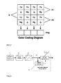
- the CCD sensor has various cells for color and brightness detection, hereinafter referred to as pixels (Cy, Ye, Mg, G), which are arranged in a matrix structure. This matrix structure is constructed in the vertical direction and in the horizontal direction.
- the pixels are divided into four color component units (Cy, Ye, Mg, G). Out of these four Color component units then determine the brightness values and the colors of the recorded image in a further calculation step.
- the pixels are arranged in an alternating arrangement according to their color components in the vertical direction of the matrix structure. The determination of the image from the martix structure will be discussed in more detail below.
- the CCD sensor has several vertical and one horizontal shift register.
- the individual pixels are transferred to the associated vertical registers, and transferred by line-by-line shifting to the horizontal readout register, from which the pixels are then read out sequentially.
- the CCD sensor in particular the color pixels (Cy, Ye, Mg, G) are arranged in terms of color in the mosaic filter as follows, in the horizontal direction two color pixels (Cy, Ye) are arranged alternately, which means that first a first color pixel (Cy ) and horizontally following a second color pixel (Ye) and then another pixel (Cy) with the first color is arranged.
- the color pixel (Mg) closes under the first color pixel (Cy), then again the first color pixel (Cy), then the third color pixel (G), then the first color pixel (Cy) and then the second color pixel (Mg ) and then the first color pixel (Cy).
- the pixels (Mg, G) are arranged alternately in the second horizontal line of the matrix.
- the first horizontal arrangement of the pixels (Cy, Ye) then follows in the vertical direction.
- the further arrangement in the martix structure then takes place alternately according to the first and second lines of the matrix, the pixels (Mg, G) being alternately interchanged in every second horizontal line.
- the sensor thus offers the possibility of detecting four colors, which can then be converted into the basic colors red, green and blue in a computing process. Each cell is able to store as a charge depending on the wavelengths of the incident light that hit it.
- This charge is converted into a voltage that indicates the intensity of the color.
- the cells are electrically separated from each other.
- FIG. 2 again shows a section of the arrangement of the pixels (Cy, Ye, Mg, G) in the CCD sensor with a color mosaic filter, with the designations from FIG. A matrix arrangement of four by four, consequently sixteen pixels is shown.
- the matrix has the arrangement of the pixels of four different color components (Cy, Ye, Mg, G).
- the chrominance signal color signal
- the luminance signal luminance signal
- FIG. 3 shows a schematic block diagram of the device according to the invention.
- the individual pixels are read out of the CCD sensor 31 and passed over a sample & hold element 32.
- the analog signal present is then converted into a digital signal by an A / D converter 33.
- These digital signals are then fed to the detection compensation device 34, consisting of the pixel error detection unit 35 and the pixel error correction unit 36.
- the device for pixel error detection and pixel error compensation is explained in more detail in FIG.
- This device consists of a pixel error controller 41 and four register stages R1, R2, R3, R4, a multiplexer Mux and an averager 42.
- the video signal is added to the device line by line, ie in the present example in a horizontal pixel sequence.
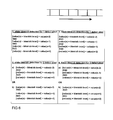
- the device detects the current state of the current pixel and four further pixels, namely the two pixels lying ahead of this pixel from the horizontal register, and two pixels following the current pixel. This is illustrated in FIG. 6 illustrated again clearly.
- the pixels are read out in a horizontal sequence and then fed to the device according to the invention.
- the current pixel is called pixel (s).
- These five pixels are compared in the pixel error control unit 41, with a predefined error barrier, in FIG. 4 and FIG. 6 denoted by blemish level.
- the comparison rules for the detection of pixel errors which lead to dark spots in the image due to loss of charge, as well as for pixels which lead to bright spots in the image due to overloading, are carried out by the pixel error control unit 41.
- the error barrier is set externally to the pixel error control unit 41, or this value is predetermined. This value can be changed.
- the error limit given to the pixel error control unit 41 is adjustable and can be changed at any time.
- a pixel error which has arisen as a result of charge loss and is recognized by the pixel error control unit 41 and is represented in the image as a dark point, is present if [Value (Pixel (n)) + blemish level] ⁇ Value (Pixel (n-2)) AND [Value (Pixel (n)) + blemish level] ⁇ Value (Pixel (n-1)) AND [Value (pixel (s)) + blemish level] ⁇ value (pixel (n + 1)) AND [Value (pixel (s)) + blemish level] ⁇ value (pixel (n + 2)), where the value (pixel (s)) is the current absolute charge-proportional voltage value determined from the horizontal register for the pixel (s) of the CCD sensor.
- a pixel error which has arisen due to overloading and is recognized by the pixel error control unit 41 and is represented in the image as a bright point, is present if [Value (Pixel (n)) - blemish level]> Value (Pixel (n-2)) AND [Value (Pixel (n)) - blemish level]> Value (Pixel (n-1)) AND [Value (Pixel (n)) - blemish level]> Value (Pixel (n + 1)) AND [Value (Pixel (n)) - blemish level]> Value (Pixel (n + 2)), where again the value (pixel (s)) denotes the current absolute charge-proportional voltage value for the pixel (n) determined from the horizontal register of the CCD sensor.
- the pixel error control unit 41 recognizes two successive pixel errors of two successive pixels in the horizontal position of the CCD sensor, which result from two successive overloaded pixels, as such, if applicable ⁇ [Value (Pixel (n)) - blemish level]> Value (Pixel (n-2)) AND [Value (Pixel (n)) - blemish level]> Value (Pixel (n-1)) AND [Value (Pixel (n)) - blemish level]> Value (Pixel (n + 2)) ⁇ OR ⁇ [Value (Pixel (n)) - blemish level]> Value (Pixel (n-2)) AND [Value (Pixel (n)) - blemish level]> Value (Pixel (n + 1)) AND [Value (Pixel (n)) - blemish level]> Value (Pixel (n + 2)) ⁇ where again
- the pixel error control unit 41 recognizes two successive pixel errors of two successive pixels in the horizontal position of the CCD sensor, which result from the loss of charge of two successive pixels, if such applies ⁇ [Value (pixel (n)) + blemish level] ⁇ value (pixel (n-2)) AND [Value (Pixel (n)) + blemish level] ⁇ Value (Pixel (n-1)) AND [Value (pixel (s)) + blemish level] ⁇ value (pixel (n + 2)) ⁇ OR ⁇ [Value (pixel (n)) + blemish level] ⁇ value (pixel (n-2)) AND [Value (pixel (s)) + blemish level] ⁇ value (pixel (n + 1)) AND [Value (pixel (s)) + blemish level] ⁇ value (pixel (n + 2)) ⁇ where again the value (pixel (s)) denotes the current absolute charge-proportional voltage value for the pixel (n
- the pixel errors are compensated for either by using the previous or subsequent value of this pixel that was not recognized as defective for a detected pixel error, or by averaging the previous or subsequent pixel values.
- the mean value is formed from pixel values of pixels (n-2) and (n + 2) and is used for a detected pixel error, regardless of whether it is a simple pixel error or a double pixel error.
- the invention provides for the pixel error correction unit to be connected in series in succession. In this way it is possible to recognize and compensate for one pixel error, two pixel errors or more pixel errors in succession.
- This is illustrated in the exemplary embodiment according to FIG. 5, in which the pixel values from the horizontal register of the CCD sensor are first introduced into a pixel error correction unit for correcting one-pixel errors. These values are then fed to a pixel error correction device for two-pixel errors.
- the proposed device is expanded in an additional combination of the pixel error units.
- the invention can also be used on black / white CCD sensors without a color filter or other sensors with a different color matrix than that shown in FIG. 1.
Landscapes
- Engineering & Computer Science (AREA)
- Multimedia (AREA)
- Signal Processing (AREA)
- Transforming Light Signals Into Electric Signals (AREA)
Applications Claiming Priority (2)
| Application Number | Priority Date | Filing Date | Title |
|---|---|---|---|
| DE10209552A DE10209552A1 (de) | 2002-03-04 | 2002-03-04 | Verfahren und Vorrichtung zur Kompensation defekter Pixel eines CCD-Sensors |
| DE10209552 | 2002-03-04 |
Publications (2)
| Publication Number | Publication Date |
|---|---|
| EP1343311A2 true EP1343311A2 (fr) | 2003-09-10 |
| EP1343311A3 EP1343311A3 (fr) | 2006-10-04 |
Family
ID=27740632
Family Applications (1)
| Application Number | Title | Priority Date | Filing Date |
|---|---|---|---|
| EP03004413A Ceased EP1343311A3 (fr) | 2002-03-04 | 2003-02-27 | Méthode et appareil de compensation des pixels défectueux d'un capteur à transfert de charge |
Country Status (2)
| Country | Link |
|---|---|
| EP (1) | EP1343311A3 (fr) |
| DE (1) | DE10209552A1 (fr) |
Cited By (4)
| Publication number | Priority date | Publication date | Assignee | Title |
|---|---|---|---|---|
| EP1777940A2 (fr) | 2005-10-18 | 2007-04-25 | Ricoh Company, Ltd. | Méthode et dispositif de réduction du bruit d'image |
| EP1863272A1 (fr) * | 2006-05-29 | 2007-12-05 | STMicroelectronics (Research & Development) Limited | Correction de pixels défectueux adjacents pour des capteurs d'image |
| WO2010017241A3 (fr) * | 2008-08-05 | 2010-04-01 | Qualcomm Incorporated | Détection de groupes de pixels altérés |
| DE102009008770A1 (de) | 2009-02-13 | 2010-08-19 | Hella Kgaa Hueck & Co. | Verfahren und Vorrichtung zur Detektion mindestens eines fehlerhaften Bildpunkterfassungselements eines Bilderfassungsbereichs eines Bilderfassungssensors |
Families Citing this family (3)
| Publication number | Priority date | Publication date | Assignee | Title |
|---|---|---|---|---|
| DE102006040349B4 (de) * | 2006-08-29 | 2016-11-10 | Robert Bosch Gmbh | Verfahren und Vorrichtung zur Erkennung von defekten Pixeln eines Bildaufnahmesensors in einem Fahrerassistenzsystem |
| JP5913934B2 (ja) * | 2011-11-30 | 2016-05-11 | キヤノン株式会社 | 画像処理装置、画像処理方法およびプログラム、および画像処理装置を有する撮像装置 |
| DE102015114009A1 (de) * | 2015-08-24 | 2017-03-02 | Rheinmetall Defence Electronics Gmbh | Verfahren und Vorrichtung zur Verarbeitung von Störpixeln auf einer Detektorfläche eines Bilddetektors |
Citations (2)
| Publication number | Priority date | Publication date | Assignee | Title |
|---|---|---|---|---|
| JPH06205302A (ja) | 1993-01-06 | 1994-07-22 | Matsushita Electric Ind Co Ltd | 画素欠陥補正装置 |
| JPH11355667A (ja) | 1998-06-05 | 1999-12-24 | Fuji Film Microdevices Co Ltd | 画素信号処理装置 |
Family Cites Families (5)
| Publication number | Priority date | Publication date | Assignee | Title |
|---|---|---|---|---|
| US4253120A (en) * | 1979-12-05 | 1981-02-24 | Rca Corporation | Defect detection means for charge transfer imagers |
| US4541116A (en) * | 1984-02-27 | 1985-09-10 | Environmental Research Institute Of Mi | Neighborhood image processing stage for implementing filtering operations |
| EP0496573B1 (fr) * | 1991-01-24 | 1995-12-20 | Matsushita Electric Industrial Co., Ltd. | Circuit pour l'élimination de défauts des éléments d'images pour détecteur d'image en technique état solide |
| US5392070A (en) * | 1991-11-26 | 1995-02-21 | Kabushiki Kaisha Toshiba | Apparatus for correcting faulty pixel signals by replacing the faulty pixel signals with normal pixel signals |
| DE60004595T2 (de) * | 1999-03-15 | 2004-03-18 | Texas Instruments Inc., Dallas | Filterung defekter Bildelemente bei digitalen Bildgebern |
-
2002
- 2002-03-04 DE DE10209552A patent/DE10209552A1/de not_active Withdrawn
-
2003
- 2003-02-27 EP EP03004413A patent/EP1343311A3/fr not_active Ceased
Patent Citations (2)
| Publication number | Priority date | Publication date | Assignee | Title |
|---|---|---|---|---|
| JPH06205302A (ja) | 1993-01-06 | 1994-07-22 | Matsushita Electric Ind Co Ltd | 画素欠陥補正装置 |
| JPH11355667A (ja) | 1998-06-05 | 1999-12-24 | Fuji Film Microdevices Co Ltd | 画素信号処理装置 |
Cited By (9)
| Publication number | Priority date | Publication date | Assignee | Title |
|---|---|---|---|---|
| EP1777940A2 (fr) | 2005-10-18 | 2007-04-25 | Ricoh Company, Ltd. | Méthode et dispositif de réduction du bruit d'image |
| EP1777940A3 (fr) * | 2005-10-18 | 2009-07-29 | Ricoh Company, Ltd. | Méthode et dispositif de réduction du bruit d'image |
| US7983508B2 (en) | 2005-10-18 | 2011-07-19 | Ricoh Company, Ltd. | Method and apparatus for image processing capable of effectively reducing an image noise |
| EP1863272A1 (fr) * | 2006-05-29 | 2007-12-05 | STMicroelectronics (Research & Development) Limited | Correction de pixels défectueux adjacents pour des capteurs d'image |
| US8036483B2 (en) | 2006-05-29 | 2011-10-11 | Stmicroelectronics (Research & Development) Limited | Couplet correction in image sensors |
| WO2010017241A3 (fr) * | 2008-08-05 | 2010-04-01 | Qualcomm Incorporated | Détection de groupes de pixels altérés |
| CN102113310A (zh) * | 2008-08-05 | 2011-06-29 | 高通股份有限公司 | 不良像素群集的检测 |
| US8971659B2 (en) | 2008-08-05 | 2015-03-03 | Qualcomm Incorporated | Bad pixel cluster detection |
| DE102009008770A1 (de) | 2009-02-13 | 2010-08-19 | Hella Kgaa Hueck & Co. | Verfahren und Vorrichtung zur Detektion mindestens eines fehlerhaften Bildpunkterfassungselements eines Bilderfassungsbereichs eines Bilderfassungssensors |
Also Published As
| Publication number | Publication date |
|---|---|
| DE10209552A1 (de) | 2003-10-02 |
| EP1343311A3 (fr) | 2006-10-04 |
Similar Documents
| Publication | Publication Date | Title |
|---|---|---|
| DE60314692T2 (de) | Digitalbildverfahren und -vorrichtung zum Zusammenfügen von Entfernung des Mosaikeffekts und Korrektur von schlechten Pixeln | |
| DE60013102T2 (de) | Schneller deterministischer ansatz zum detektieren von defekten pixels in einem bildsensor | |
| DE69105815T2 (de) | Fehlerkorrektur für CCD- und CID-Bilderzeugungsvorrichtungen. | |
| DE3600330C2 (de) | Dreifarben-Kathodenstrahlröhrenanordnung | |
| DE3632487C2 (fr) | ||
| DE19619734C2 (de) | Elektronisches Endoskopsystem | |
| DE3852467T2 (de) | Defektkompensation für Festkörperkameras. | |
| DE69828046T2 (de) | Erweiterter dynamikbereich für bildformungssystem und verfahren | |
| DE69314370T2 (de) | Festkörperbildaufnahmevorrichtung mit automatischer Korrektur defekter Bildelemente | |
| DE3229771C2 (fr) | ||
| DE60203869T2 (de) | Verfahren zur schnellen automatischen Belichtungs- oder Verstärkungsregelung in einem MOS Bildsensor | |
| DE3632488C2 (fr) | ||
| DE20019915U1 (de) | Dynamische Erkennung und Korrektur von anomalen Pixeln | |
| DE69923048T2 (de) | Wirksames Testverfahren zum Klassifizieren der Bildqualität eines optischen Sensors unter Verwendung von drei Pixelkategorien | |
| DE602005005553T2 (de) | Abbildungsvorrichtung und Abbildungsverfahren | |
| DE68927389T2 (de) | Videospezialeffekte | |
| DE102016117584A1 (de) | Videobildgebungssystem | |
| DE102007050896A1 (de) | Elektronisches Endoskop | |
| DE10344397B4 (de) | Vorrichtung und Verfahren zur Kantenhervorhebung bei der Bildverarbeitung | |
| DE4106825A1 (de) | Belichtungskontrollvorrichtung fuer einzelbild-videokameras | |
| DE102013012810A1 (de) | Verfahren zum Aktivieren und Deaktivieren einer Bildkorrekturfunktion, Kamerasystem und Kraftfahrzeug | |
| DE4329839A1 (de) | Abbildungseinrichtung mit zwei Bildsensoren | |
| EP2367360A2 (fr) | Procédé de correction des erreurs de couleur dans les images de caméras numériques de couleur | |
| DE102013115000A1 (de) | Blendungsminderung für dynamischen Rückspiegel | |
| EP3809691B1 (fr) | Procédé de reconnaissance et de correction d'erreurs d'image ainsi qu'unité de traitement des images et programme informatique associé |
Legal Events
| Date | Code | Title | Description |
|---|---|---|---|
| PUAI | Public reference made under article 153(3) epc to a published international application that has entered the european phase |
Free format text: ORIGINAL CODE: 0009012 |
|
| AK | Designated contracting states |
Kind code of ref document: A2 Designated state(s): AT BE BG CH CY CZ DE DK EE ES FI FR GB GR HU IE IT LI LU MC NL PT SE SI SK TR |
|
| AX | Request for extension of the european patent |
Extension state: AL LT LV MK RO |
|
| RAP1 | Party data changed (applicant data changed or rights of an application transferred) |
Owner name: FUNKWERK PLETTAC ELECTRONIC GMBH |
|
| PUAL | Search report despatched |
Free format text: ORIGINAL CODE: 0009013 |
|
| AK | Designated contracting states |
Kind code of ref document: A3 Designated state(s): AT BE BG CH CY CZ DE DK EE ES FI FR GB GR HU IE IT LI LU MC NL PT SE SI SK TR |
|
| AX | Request for extension of the european patent |
Extension state: AL LT LV MK RO |
|
| 17P | Request for examination filed |
Effective date: 20070404 |
|
| AKX | Designation fees paid |
Designated state(s): AT BE BG CH CY CZ DE DK EE ES FI FR GB GR HU IE IT LI LU MC NL PT SE SI SK TR |
|
| 17Q | First examination report despatched |
Effective date: 20070614 |
|
| STAA | Information on the status of an ep patent application or granted ep patent |
Free format text: STATUS: THE APPLICATION HAS BEEN REFUSED |
|
| 18R | Application refused |
Effective date: 20100504 |