EP1347532B1 - Leistungsteiler/-kombinierer - Google Patents
Leistungsteiler/-kombinierer Download PDFInfo
- Publication number
- EP1347532B1 EP1347532B1 EP03100647A EP03100647A EP1347532B1 EP 1347532 B1 EP1347532 B1 EP 1347532B1 EP 03100647 A EP03100647 A EP 03100647A EP 03100647 A EP03100647 A EP 03100647A EP 1347532 B1 EP1347532 B1 EP 1347532B1
- Authority
- EP
- European Patent Office
- Prior art keywords
- port
- power divider
- transmission line
- combiner according
- combiner
- Prior art date
- Legal status (The legal status is an assumption and is not a legal conclusion. Google has not performed a legal analysis and makes no representation as to the accuracy of the status listed.)
- Expired - Lifetime
Links
- 230000005540 biological transmission Effects 0.000 claims abstract description 114
- 238000009413 insulation Methods 0.000 claims description 9
- 239000010410 layer Substances 0.000 description 93
- 239000002184 metal Substances 0.000 description 19
- 238000007747 plating Methods 0.000 description 19
- 238000000034 method Methods 0.000 description 4
- 239000000919 ceramic Substances 0.000 description 3
- 238000005516 engineering process Methods 0.000 description 3
- 239000002344 surface layer Substances 0.000 description 3
- 238000010586 diagram Methods 0.000 description 2
- 238000005530 etching Methods 0.000 description 2
- 239000010408 film Substances 0.000 description 2
- 239000000758 substrate Substances 0.000 description 2
- 239000010409 thin film Substances 0.000 description 2
- ATJFFYVFTNAWJD-UHFFFAOYSA-N Tin Chemical compound [Sn] ATJFFYVFTNAWJD-UHFFFAOYSA-N 0.000 description 1
- PNEYBMLMFCGWSK-UHFFFAOYSA-N aluminium oxide Inorganic materials [O-2].[O-2].[O-2].[Al+3].[Al+3] PNEYBMLMFCGWSK-UHFFFAOYSA-N 0.000 description 1
- 229910010293 ceramic material Inorganic materials 0.000 description 1
- 230000001419 dependent effect Effects 0.000 description 1
- 230000002542 deteriorative effect Effects 0.000 description 1
- 239000011521 glass Substances 0.000 description 1
- 238000002955 isolation Methods 0.000 description 1
- 239000007788 liquid Substances 0.000 description 1
- 239000000463 material Substances 0.000 description 1
- 239000000203 mixture Substances 0.000 description 1
Images


Classifications
-
- H—ELECTRICITY
- H01—ELECTRIC ELEMENTS
- H01P—WAVEGUIDES; RESONATORS, LINES, OR OTHER DEVICES OF THE WAVEGUIDE TYPE
- H01P5/00—Coupling devices of the waveguide type
- H01P5/12—Coupling devices having more than two ports
- H01P5/16—Conjugate devices, i.e. devices having at least one port decoupled from one other port
Definitions
- the invention relates to radio frequency technology and particularly to power management arrangements used in radio and microwave frequency ranges.
- Power dividers/combiners operating in high frequency ranges are used either to divide or combine radio and microwave signals.
- a power divider typically comprises an input port and two output ports. The power to the input port is distributed to the output ports evenly or in another proportion. In a power combiner, several input signals are combined into one output signal.
- a power divider/combiner according to the prior art is represented by what is called a Wilkinson power divider/combiner.
- a Wilkinson power divider/combiner there is a conductive pattern upon an insulating substrate structure, such as a printed board.
- the conductive pattern comprises transmission lines of a length of ⁇ /4 between the input port and the output ports.
- Qualities required of power dividers/combiners include small power losses, sufficient insulation between the transmission lines and sufficient EMC protection.
- An example of a Wilkinson power divider is described in a document by Nishikawa K. et al: " Miniaturized Wilkinson power divider using three-dimensional MMIC technology", IEEE Microwave and guided wave letters, IEEE INC, New York, US, vol. 6, no. 10, 1 October 1996, pages 373-374 or in US-A-5,650,756.
- the Wilkinson power dividers/combiners according to the prior art are large in size and take too much space from the surface layer of the printed board in order for them to be integrated into recent devices requiring increasingly small components. It is difficult to reduce the size of the Wilkinson power dividers/combiners without, for example, deteriorating the insulation between transmission lines and increasing power losses too much.
- An object of the invention is thus to implement a power management arrangement in such a way that an arrangement is achieved which has a small size but yet a good insulating capacity and small power losses.
- a power management arrangement which comprises, formed as a multilayer structure, several insulating layers; several conductive layers functioning as reference planes; a first port, a second port and a third port; a first transmission line from the first port to the second port; a second transmission line from the first port to the third port; means for connecting the transmission lines to the ports; at least one passive element between the second and third ports.
- the first transmission line is in a layer other than the one where the second transmission line is.
- the invention is based on the transmission lines of the power management arrangement being in different layers.
- a plurality of advantages is achieved with the power management arrangement according to the invention. Good isolation is achieved between the branches of the different transmission lines in the power management arrangement. Owing to the reference plane structures used in the solution according to the invention, also power losses are reduced and the EMC (Electromagnetic Compatibility) protection is improved. Space is also saved significantly in the surface layer of the printed board.
- EMC Electromagnetic Compatibility
- FIG. 1 shows a simplified block diagram of a phase-locked circuit 90 which utilizes a Wilkinson power divider implementing the power management arrangement.
- Phase-locked circuits are widely used in telecommunication systems.
- the phase-locked circuit is responsible for generating an oscillator signal with sufficient frequency stability and a sufficiently small amount of noise for the receiver and transceiver of a telecommunication system.
- the phased-locked circuit 90 comprises a voltage-controlled oscillator (VCO) 94, a Wilkinson power divider 92, an output amplifier 96, a synchronizer 98 and a filter 99.
- the voltage-controlled oscillator 94 generates output power as a response to the input voltage.
- the Wilkinson power divider 92 is needed for distributing the output power generated by the oscillator to the output amplifier 96 and to the loop comprised by the synchronizer 98 and the filter 99.
- the filter 99 is usually a low-pass filter, which can be implemented by using amplifiers, resistances and capacitances, for instance.
- FIG. 2 shows a perspective view of a Wilkinson power divider according to the presented solution.
- the power divider according to Figure 2 is designed to function at a medium frequency of 1,8 GHz.
- the Wilkinson power divider according to Figure 2 comprises, formed as a multilayer structure 100, several insulating layers 130, 132, 134, 136; several conductive layers 124, 126, 128; a first port 101, a second port 102 and a third port 104; a first transmission line 106 and a second transmission line 108; a passive element 116 and several lead-throughs 110, 112, 114, 122 in insulating layers 132, 134, 136 and in conductive layers 126, 128.
- the first transmission line 106 is in the second uppermost insulating layer 134 and the second transmission line 108 is in the lowest insulating layer 130.
- the middle conductive layer 126 of the conductive layers 124, 126, 128 functioning as reference planes is in the area between the first and the second transmission line 106, 108.
- the conductive layers 124, 126, 128 functioning as reference planes are, in practice, ground planes.
- the insulating layers 130, 132, 134, 136 of the multilayer structure 100 in the example of Figure 2 are implemented by means of ceramic technologies known as such, for example LTCC (Low Temperature Cofired Ceramic) or HTCC (High Temperature Cofired Ceramic).
- the insulating layers 130, 132, 134, 136 can be implemented with organic printed board materials according to the prior art.
- the ceramic material used in implementing the insulating layers 130, 132, 134, 136 is, for instance, a mixture of alumina and glass.
- the thickness of each insulating layer 130, 132, 134, 136 is preferably 0.4 mm, the dielectric constant being 7.7.
- the multilayer structure 100 comprises three conductive layers 124, 126, 128 functioning as reference planes.
- the conductive layers 124, 126, 128 are located in the multilayer structure 100 in such a way that there are two uppermost insulating layers 134, 136 between the middle and the uppermost conductive layer 126, 128 and two lowest insulating layers 130, 132 between the lowest and the middle conductive layer 124, 126, whereby, according to Figure 2, the areas on the lower and upper surface of the multilayer structure 100 are conductive layers 124, 128, and the layer in the middle of the four insulating layers 130, 132, 134, 136 of the multilayer structure 100 is a conductive layer 126.
- the thickness of each conductive layer 124, 126, 128 is preferably 10 ⁇ m.
- the first port 101 Upon the second lowest insulating layer 132 in the multilayer structure 100, there is the first port 101, which functions as an input port.
- the first port 101 preferably comprises a strip line of 50 ⁇ .
- the width of the first port 101 is preferably 380 ⁇ m.
- the second port 102 and the third port 104 Upon the uppermost insulating layer 136 in the multilayer structure 100, there are the second port 102 and the third port 104.
- the second and the third port 102, 104 function as output ports.
- the second and the third port 102, 104 preferably comprise strip lines of 50 ⁇ .
- the widths of the second and the third port 102, 104 are preferably 460 ⁇ m.
- the power management arrangement could also be used for power combining instead of power dividing, in which case the first port 101 would function as an output port and, correspondingly, the second and the third port 102, 104 would function as input ports.
- a passive element 116 is mounted between the second and the third port 102, 104, which element is in the example of Figure 2 preferably a resistor of 100 ⁇ . The purpose of the passive element 116 is to improve the insulation between the second and the third port 102, 104.
- the transmission lines 106, 108 are strip lines of a length of ⁇ /4.
- the impedances of the first, second and third ports 101, 102, 104 being Zo
- the impedance of the transmission lines 106, 108 can, in the example, be calculated by multiplying Zo by square root two.
- the characteristic impedance of the transmission lines 106, 108 is preferably 70.7 ⁇ when the impedances of the ports 101, 102 and 104 are 50 ⁇ .
- the widths of the transmission lines 106, 108 are preferably 80 ⁇ m.
- the lead-throughs 110, 112, 114, 122 are plated-through, preferably filled with liquid tin, whereby they form the required connections between the ports 101, 102, 104 and the transmission lines 106, 108.
- the lead-throughs 110, 112, 114, 122 are preferably impedance-matched.
- the first port 101 is connected to the transmission lines 106, 108 with the lead-throughs 110, 122 formed through the insulating layers 132, 134 and with conductive metal platings formed in the lead-throughs.
- the first transmission line 106 is by one end 146c thereof connected to the second port 102 by means of a conductive metal plating formed in the lead-through 112 leading through the uppermost insulating layer 136.
- the second transmission line is, in turn, connected by one end 156c thereof to the third port 104 with a conductive metal plating formed in the lead-through 114 leading through the insulating layers 132, 134, 136.
- both transmission lines 106, 108 are in the form of successive branches 140 to 146, 150 to 156 to save space.
- the successive branches 140 to 146, 150 to 156 comprise diverging areas 140a to 146a, 150a to 156a distancing towards the outer edges of the insulating layers 130, 134 and returning areas 140c to 146c, 150c to 156c re-approaching the middle area of the insulating layers 130, 134, as well as turning areas 140b to 146b, 150b to 156b between the diverging and the returning areas.
- the turning areas 140b to 146b, 150b to 156b preferably form an angle of 90° relative to the diverging and returning areas.
- the conductive patterns formed by the transmission lines 106, 108 are implemented in manners known as such, preferably with thin-film or thick-film techniques. Alternatively, the conductive patterns formed by the transmission lines 106, 108 can be implemented with growing or etching techniques.
- the diverging area 140a of the first branch 140 of the transmission line 106 is connected to the first port 101 with a conductive metal plating formed in the lead-through 110, and the diverging area 150a of the first branch 150 of the transmission line 108 is connected to the first port 101 with a conductive metal plating formed in the lead-through 122.
- the first diverging areas 140a, 150a of the transmission lines 106, 108, starting at the first port 101 are on different sides of the first port 101 in such a way that the first diverging areas 140a, 150a are not physically superposed.
- the turning areas 140b to 146b, 150b to 156b of two successive branches 140 to 146, 150 to 156 are in the example on different sides of the first port 101.
- the distance between the parallel areas of the branches 140, 142, 144, 146, 151, 153, 155 on the left side of the first port 101 is in the example 200 ⁇ m.
- the distance between the parallel areas of the branches 141, 143, 145, 150, 152, 154, 156 on the right side of the first port 101 is also 200 ⁇ m.
- the branches 140 to 146, 150 to 156 of the first and the second transmission line 106, 108 are parallel to each other.
- the form of the transmission lines 106, 108 which comprises the branches 140 to 146, 150 to 156, enables significant saving in space in the Wilkinson power divider.
- the transmission lines 106, 108 have been positioned in different layers of the multilayer structure 100, a significantly large space becomes free on the uppermost insulating layer 136 of the multilayer structure 100.
- the Wilkinson power divider takes up to 90 % less space on the uppermost insulating layer 136 than it would take if the transmission lines 106, 108 were in the same layer of the multilayer structure 100.
- the transmission lines 106, 108 are located superposed in the multilayer structure 100.
- the transmission lines 106, 108 are in different layers preferably in such a way that those areas of the branches 140 to 146, 150 to 156 of the first and the second transmission line 106, 108 that are headed towards opposite directions are superposed.
- the reference planes functioning as the conductive layers 124, 126, 128 in the example of Figure 2 form strip line configurations with the transmission lines 106, 108 and the microstrips of the first port 101.
- a strip line typically comprises a strip line between two reference planes.
- the lowest conductive layer 124 and the middle conductive layer 126 function as reference planes for the second transmission line 108.
- the two lowest insulating layers 130, 132 function as the insulation of the strip line configuration.
- the lowest conductive layer 124 and the uppermost conductive layer 128 function as reference planes for the first port 101.
- the middle and the uppermost conductive layer 126, 128 function as reference plane layers for the first transmission line 106.
- the middle conductive layer 126, the strip lines of the second and the third port 102, 104 and the insulating layers 134, 136 form microstrip line configurations.
- a microstrip line comprises a strip line and a reference plane, between which there is an insulating substrate 130, 132, 134, 136.
- the middle conductive layer 126 functions as a reference plane for both the second and the third port 102, 104.
- Connecting the conductive layers 124, 126, 128, which function as reference plane layers, to the transmission lines 106, 108 and to the ports 101, 102, 104 is implemented with conductive metal platings formed in the lead-throughs 120 in the multilayer structure 100.
- the lead-throughs 120 have been omitted from Figure 2.
- the second and the third port 102, 104 can alternatively be located upon the second lowest insulating layer 132, whereby the lowest conductive layer 124 and the uppermost conductive layer 128 function as reference planes for the ports 102, 104.
- the second and the third port 102, 104 form strip line configurations with the conductive layers 124, 128.
- Figure 3 shows a top view of a detail of a Wilkinson power divider according to a preferred embodiment of the invention.
- the example of Figure 3 is similar to the Wilkinson power divider shown in Figure 2, but Figure 3 is simplified in such a way that the conductive layers 124, 126, 128 and the insulating layers 130, 132, 134, 136 have been omitted.
- Figure 3 indicates with areas limited by broken lines those lead-throughs 120 that have conductive metal platings by means of which the connection of the conductive layers 124, 126, 128 to the transmission lines 106, 108 and the ports 101, 102, 104 is implemented.
- the first port 101 is connected to the transmission line 106 upon the second uppermost insulating layer 134 by means of a conductive metal plating formed in the lead-through 110.
- the transmission line 108 upon the lowest insulating layer 130 is connected to the first port 101 by means of a conductive metal plating formed in the lead-through 122.
- the lead-through 122 is, however, under the lead-through 110 of the first port 101.
- the transmission lines 106, 108 comprise successive branches 140 to 146, 150 to 156 also in Figure 3.
- the second transmission line 108 is, however, partly under the first transmission line 106 positioned in the upper layer in such a way that it cannot be seen completely from above.
- the first branches 140, 150 of the transmission lines 106, 108, starting at the first port 101 must be on different sides of the first port 101 so that the diverging areas 140a, 150a of the first branches 140, 150 are not physically superposed.
- Figure 4 shows a side view of a detail of a Wilkinson power divider according to Figures 2 and 3.
- Those lead-throughs 120 that have conductive metal platings by means of which the connection of the conductive layers 124, 126, 128 to the transmission lines 106, 108 and the ports 101, 102, 104 is implemented are not indicated in Figure 4.
- Figure 4 shows the four insulating layers 130, 132, 134, 136 of the multilayer structure 100; the three layers 124, 126, 128 functioning as reference planes; the first and the third port 101, 104; the first and the second transmission line 106, 108; and lead-throughs 110, 114, 122.
- the conductive layers 124, 126, 128 seen in Figure 4 are below and above the insulating layers 130, 132, 134, 136 and between them.
- the first port 101 connected to the first transmission line 106 upon the second uppermost insulating layer by means of a conductive metal plating formed in the lead-through 110 and to the second transmission line 108 upon the lowest insulating layer 130 by means of a conductive metal plating formed in the lead-through 122.
- the transmission lines 106, 108 lead in a planar manner from the lead-throughs 110, 112 of the first port 101 to the lead-throughs 112, 114 of the second and third ports 102, 104.
- the second port 102 and the lead-through 112 connecting the first transmission line 106 to the second port 102 are not seen in Figure 4, because they are behind the third port 104 and the lead-through 114 connecting the second transmission line 108 to the third port 104.
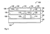
- Figure 5 shows a front view of the example of Figures 2, 3 and 4.
- Those lead-throughs 120 that have conductive metal platings by means of which the connection of the conductive layers 124, 126, 128 to the transmission lines 106, 108 and the ports 101, 102, 104 is implemented are not indicated here either.
- Figure 5 shows the four insulating layers 130, 132, 134, 136 of the multilayer structure 100; the three conductive layers 124, 126, 128 functioning as reference planes; the first, the second and the third port 101, 102, 104; the first and the second transmission line 106, 108; and the lead-throughs 110, 112, 114, 122.
- the conductive layers 124, 126, 128 seen in Figure 5 are below and above the insulating layers 130, 132, 134, 136 and between them.
- the first port 101 Upon the second lowest insulating layer 132, there is the first port 101 connected to the first transmission line 106 upon the third insulating layer 134 by means of a conductive metal plating formed in the lead-through 110 and to the second transmission line 108 upon the first insulating layer 130 by means of a conductive metal plating formed in the lead-through 122.
- the middle conductive layer 126 functioning as a reference plane for the first and the second transmission line 106, 108 and for the second and the third port 102, 104.
- the second and the third port 102, 104 are upon the uppermost insulating layer 136.
- the conductive layer 124 positioned below the first insulating layer 130 functions as a reference plane for the second transmission line 108 and the first port 101.
- the first transmission line 106 is connected to the second port 102 positioned upon the uppermost insulating layer 136 by means of a conductive metal plating formed in the lead-through 112.
- the second transmission line 108 is, in turn, connected to the third port 104 by means of a conductive metal plating formed in the lead-through 114.
- Figure 6 shows a perspective view of another example according to the invention.
- the Wilkinson power divider according to the example of Figure 6 formed as a multilayer structure 100, comprises several conductive layers 124, 126, 128 functioning as reference planes; the first port 101, the second port 102 and the third port 104; the first transmission line 106 and the second transmission line 108; a passive element 116; and several lead-throughs 110, 112, 114, 122.
- the second uppermost insulating layer 134 in the multilayer structure 100 there is the first transmission line 106.
- the second transmission line 108 is, in turn, upon the lowest insulating layer 130.
- the conductive patterns formed by the transmission lines 106, 108 of the example of Figure 6 are implemented in manners known per se, preferably with thin-film or thick-film techniques. Alternatively, the conductive patterns formed by the transmission lines 106, 108 can be implemented with growing or etching techniques.
- the transmission line 106 is connected to the first port 101 by means of a conductive metal plating formed in the lead-through 110, and the transmission line 108 is connected to the first port 101 by means of a conductive metal plating formed in the lead-through 122.
- the transmission lines 106, 108 shown in Figure 6 are spiral-shaped.
- the transmission lines 106, 108 are spiral-shaped in such a way that the spiral twist in the first transmission line 106 begins to open in the opposite direction compared with the spiral twist in the second transmission line 108.
- the spiral twist in the first transmission line 106 proceeds clockwise and is connected to the second port 102 on the left side of the port.
- the spiral twist in the second transmission line 108 proceeds counter-clockwise and is connected to the third port 104 on the right side of the port.
- a passive element 116 for instance resistance, is mounted between the second and the third port 102, 104.
Landscapes
- Structure Of Printed Boards (AREA)
- Waveguides (AREA)
- Production Of Multi-Layered Print Wiring Board (AREA)
- Diaphragms For Electromechanical Transducers (AREA)
- Measuring Pulse, Heart Rate, Blood Pressure Or Blood Flow (AREA)
- Medicines Containing Material From Animals Or Micro-Organisms (AREA)
- Electroluminescent Light Sources (AREA)
Claims (23)
- Leistungsteiler/-kombinierer, umfassend, als eine Vielschichten-Struktur (100) ausgebildet:- mehrere isolierende Schichten (130, 132, 134, 136)- mehrere leitende Schichten (124, 126, 128), die als Masseplatten wirken;- einen ersten Anschluss (101), einen zweiten Anschluss (102) und einen dritten Anschluss (104);- eine erste Übertragungsleitung (106) von dem ersten Anschluss (101) zu dem zweiten Anschluss (102), eine zweite Übertragungsleitung (108) von dem ersten Anschluss (101) zu dem dritten Anschluss (104);- leitende Durchführungen (110, 112, 114, 122) in den isolierenden Schichten und in den leitenden Schichten, welche die Übertragungsleitungen (106, 108) mit den Anschlüssen (101, 102, 104) verbinden;- mindestens ein passives Element (116), welches zwischen den zweiten und den dritten Anschluss (102, 104) geschaltet ist;- wobei sich die erste Übertragungsleitung (106) auf einer anderen isolierenden Schicht (130, 132, 134, 136) befindet als die, auf welcher sich die zweite Übertragungsleitung (108) befmdet;- wobei sich mindestens eine isolierende Schicht über jeder Übertragungsleitung befindet; und wobei sich mindestens eine leitende Schicht oberhalb von jeder Übertragungsleitung befindet und mindestens eine leitende Schicht unterhalb von jeder Übertragungsleitung befindet, und- wobei sich mindestens eine der leitenden Schichten (126) in dem Bereich zwischen der ersten und der zweiten Übertragungsleitung (106, 108) befindet, um zusammen mit den anderen leitenden Schichten (124, 128) Streifenleiter-Konfigurationen mit der ersten und zweiten Übertragungsleitung (106, 108) zu bilden, und wobei die isolierenden Schichten (130, 132, 134, 136) als Isolierung für die Streifenleiter-Konfigurationen wirken.
- Leistungsteiler/-kombinierer gemäß Anspruch 1, dadurch gekennzeichnet, dass die erste Übertragungsleitung (106) in der Form von aufeinanderfolgenden Zweigen (140 bis 146) vorliegt, wobei die Zweige (140 bis 146) einen auseinanderlaufenden Bereich (140a bis 146a) und einen zurücklaufenden Bereich (140c bis 146c) umfassen.
- Leistungsteiler/-kombinierer gemäß Anspruch 1, dadurch gekennzeichnet, dass die zweite Übertragungsleitung (108) in der Form von aufeinanderfolgenden Zweigen (150 bis 156) vorliegt, wobei die Zweige (150 bis 156) einen auseinanderlaufenden Bereich (150a bis 156a) und einen zurücklaufenden Bereich (150c bis 156c) umfassen.
- Leistungsteiler/-kombinierer gemäß Anspruch 2 und 3, dadurch gekennzeichnet dass die Zweige (140 bis 146, 150 bis 156) der ersten und der zweiten Übertragungsleitung (106, 108) parallel zueinander sind.
- Leistungsteiler/-kombinierer gemäß Anspruch 1, dadurch gekennzeichnet, dass die erste und die zweite Übertragungsleitung (106, 108) übereinander liegen.
- Leistungsteiler/-kombinierer gemäß Anspruch 2 und 3, dadurch gekennzeichnet dass die Zweige (140 bis 146, 150 bis 156) der ersten und der zweiten Übertragungsleitung (106, 108) übereinander liegen.
- Leistungsteiler/-kombinierer gemäß Anspruch 2 und 3, dadurch gekennzeichnet, dass die Bereiche der Zweige (140 bis 146, 150 bis 156) der ersten und der zweiten Übertragungsleitung (106, 108), die in entgegengesetzte Richtungen verlaufen, übereinander liegen.
- Leistungsteiler/-kombinierer gemäß Anspruch 1, dadurch gekennzeichnet, dass die erste Übertragungsleitung (106) spiralförmig ist.
- Leistungsteiler/-kombinierer gemäß Anspruch 1, dadurch gekennzeichnet, dass die zweite Übertragungsleitung (108) spiralförmig ist.
- Leistungsteiler/-kombinierer gemäß Anspruch 2 und 3, dadurch gekennzeichnet, dass der auseinanderlaufende Bereich (140a) des ersten Zweigs (140) der ersten Übertragungsleitung (106) und der auseinanderlaufende Bereich (150a) des ersten Zweigs (150) der zweiten Übertragungsleitung (108) auf entgegengesetzte Ränder der Vielschichten-Struktur (100) zulaufen.
- Leistungsteiler/-kombinierer gemäß Anspruch 1, dadurch gekennzeichnet, dass der Leistungsteiler/-kombinierer ein Wilkinson-Leistungsteiler ist.
- Leistungsteiler/-kombinierer gemäß Anspruch 1, dadurch gekennzeichnet, dass der Leistungsteiler/-kombinierer ein Wilkinson-Leistungskombinierer ist.
- Leistungsteiler/-kombinierer gemäß Anspruch 1, dadurch gekennzeichnet, dass die Übertragungsleitungen (106, 108) Streifenleiter sind.
- Leistungsteiler/-kombinierer gemäß Anspruch 1, dadurch gekennzeichnet, dass der erste, der zweite und der dritte Anschluss (101, 102, 104) Streifenleiter sind.
- Leistungsteiler/-kombinierer gemäß Anspruch 1, dadurch gekennzeichnet, dass der erste Anschluss (101) und ein Teil der leitenden Schichten (124, 126, 128) eine Streifenleiter-Konfiguration bilden.
- Leistungsteiler/-kombinierer gemäß Anspruch 1, dadurch gekennzeichnet, dass der zweite Anschluss (102), ein Teil der leitenden Schichten (124, 126, 128) und ein Teil der isolierenden Schichten (130, 132, 134, 136) eine Mikrostreifenleiter-Konfiguration bilden.
- Leistungsteiler/-kombinierer gemäß Anspruch 1, dadurch gekennzeichnet, dass der zweite Anschluss (102) und ein Teil der leitenden Schichten (124, 126, 128) eine Streifenleiter-Konfiguration bilden.
- Leistungsteiler/-kombinierer gemäß Anspruch 1, dadurch gekennzeichnet, dass der dritte Anschluss (104), ein Teil der leitenden Schichten (124, 126, 128) und ein Teil der isolierenden Schichten (130, 132, 134, 136) eine Mikrostreifenleiter-Konfiguration bilden.
- Leistungsteiler/-kombinierer gemäß Anspruch 1, dadurch gekennzeichnet, dass der dritte Anschluss (104) und ein Teil der leitenden Schichten (124, 126, 128) eine Streifenleiter-Konfiguration bilden.
- Leistungsteiler/-kombinierer gemäß Anspruch 1, dadurch gekennzeichnet, dass die erste und die zweite Übertragungsleitung (106, 108) gleich lang sind.
- Leistungsteiler/-kombinierer gemäß Anspruch 1, dadurch gekennzeichnet, dass die erste und die zweite Übertragungsleitung (106, 108) eine Länge von λ/4 haben.
- Leistungsteiler/-kombinierer gemäß Anspruch 1, dadurch gekennzeichnet, dass die leitenden Durchführungen (110, 112, 114, 122), welche die Übertragungsleitungen (106, 108) mit den Anschlüssen (101, 102, 104) verbinden, impedanzangepasste Durchführungen sind.
- Leistungsteiler/-kombinierer gemäß Anspruch 1, dadurch gekennzeichnet, dass das passive Element (116) ein Widerstand ist.
Applications Claiming Priority (2)
| Application Number | Priority Date | Filing Date | Title |
|---|---|---|---|
| FI20020522 | 2002-03-19 | ||
| FI20020522A FI20020522A0 (fi) | 2002-03-19 | 2002-03-19 | Tehonhallintajärjestely |
Publications (2)
| Publication Number | Publication Date |
|---|---|
| EP1347532A1 EP1347532A1 (de) | 2003-09-24 |
| EP1347532B1 true EP1347532B1 (de) | 2006-05-31 |
Family
ID=8563599
Family Applications (1)
| Application Number | Title | Priority Date | Filing Date |
|---|---|---|---|
| EP03100647A Expired - Lifetime EP1347532B1 (de) | 2002-03-19 | 2003-03-14 | Leistungsteiler/-kombinierer |
Country Status (7)
| Country | Link |
|---|---|
| US (1) | US6861923B2 (de) |
| EP (1) | EP1347532B1 (de) |
| CN (1) | CN1236520C (de) |
| AT (1) | ATE328370T1 (de) |
| DE (1) | DE60305553T2 (de) |
| ES (1) | ES2263914T3 (de) |
| FI (1) | FI20020522A0 (de) |
Families Citing this family (21)
| Publication number | Priority date | Publication date | Assignee | Title |
|---|---|---|---|---|
| JP4636950B2 (ja) * | 2005-06-22 | 2011-02-23 | 株式会社日立メディアエレクトロニクス | 伝送回路、アンテナ共用器、高周波スイッチ回路 |
| JP2008109094A (ja) * | 2006-09-29 | 2008-05-08 | Sanyo Electric Co Ltd | 素子搭載用基板および半導体モジュール |
| JP2008252215A (ja) * | 2007-03-29 | 2008-10-16 | Soshin Electric Co Ltd | ドハティ増幅器用合成器 |
| US8216912B2 (en) | 2009-08-26 | 2012-07-10 | International Business Machines Corporation | Method, structure, and design structure for a through-silicon-via Wilkinson power divider |
| TWI639273B (zh) | 2012-05-11 | 2018-10-21 | 國立中山大學 | 堆疊電感諧振器及使用此諧振器的帶通濾波器結構 |
| TWI508361B (zh) * | 2012-07-30 | 2015-11-11 | Inpaq Technology Co Ltd | 共模訊號濾波器 |
| EP2912717B1 (de) * | 2012-10-25 | 2018-07-18 | Telefonaktiebolaget LM Ericsson (publ) | Leistungsteiler und verfahren zur herstellung davon |
| CA2875097C (en) | 2013-12-18 | 2022-02-22 | Com Dev International Ltd. | Transmission line circuit assemblies and processes for fabrication |
| CN104319448B (zh) * | 2014-10-24 | 2018-01-16 | 中国电子科技集团公司第四十一研究所 | 一种基于附电阻膜的高频印制板的多层功率分配网络 |
| CN105633537B (zh) * | 2014-11-24 | 2018-11-16 | 中国航空工业集团公司雷华电子技术研究所 | 一种带线功分器片式电阻让位孔的设计结构 |
| DE102015212232B4 (de) | 2015-06-30 | 2020-03-05 | TRUMPF Hüttinger GmbH + Co. KG | Leistungscombiner zur Kopplung von Hochfrequenzsignalen und Leistungscombineranordnung mit einem solchen Leistungscombiner |
| CN107039734B (zh) * | 2016-06-08 | 2022-04-29 | 深圳振华富电子有限公司 | 一种叠层片式功率分配模块及其制造方法 |
| CN107039735B (zh) * | 2016-06-08 | 2022-04-29 | 深圳振华富电子有限公司 | 一种叠层片式功率分配模块及其制造方法 |
| KR102554415B1 (ko) * | 2016-11-18 | 2023-07-11 | 삼성전자주식회사 | 반도체 패키지 |
| KR102299451B1 (ko) * | 2016-12-20 | 2021-09-08 | 한국전자기술연구원 | 광대역 특성을 갖는 분배/합성기 |
| US10320043B2 (en) | 2017-05-23 | 2019-06-11 | Nanning Fugui Precision Industrial Co., Ltd. | Power distributing device |
| WO2022081964A1 (en) * | 2020-10-16 | 2022-04-21 | Anokiwave, Inc. | Pinwheel three-way wilkinson power divider for millimeter wave applications |
| CN118572340A (zh) * | 2023-02-23 | 2024-08-30 | 鹏鼎控股(深圳)股份有限公司 | 功率分配器及其制作方法 |
| DE102024131929A1 (de) | 2024-10-31 | 2026-04-30 | TRUMPF Hüttinger GmbH + Co. KG | Hochfrequenz-Leistungskoppler für einen Leistungsumwandler für eine Industrieprozessanordnung |
| DE102024131926A1 (de) | 2024-10-31 | 2026-04-30 | TRUMPF Hüttinger GmbH + Co. KG | Hochfrequenz-Leistungskoppler für einen Leistungsumwandler für eine Industrieprozessanordnung |
| DE102024131930A1 (de) | 2024-10-31 | 2026-04-30 | TRUMPF Hüttinger GmbH + Co. KG | Hochfrequenz-Leistungskoppler für einen Leistungsumwandler für eine Industrieprozessanordnung |
Family Cites Families (8)
| Publication number | Priority date | Publication date | Assignee | Title |
|---|---|---|---|---|
| US5206611A (en) * | 1992-03-12 | 1993-04-27 | Krytar, Inc. | N-way microwave power divider |
| JP3333014B2 (ja) * | 1993-10-04 | 2002-10-07 | ティーディーケイ株式会社 | 高周波信号分配・合成器 |
| US5426404A (en) | 1994-01-28 | 1995-06-20 | Motorola, Inc. | Electrical circuit using low volume multilayer transmission line devices |
| US5467064A (en) | 1994-01-28 | 1995-11-14 | Motorola, Inc. | Embedded ground plane for providing shielded layers in low volume multilayer transmission line devices |
| US5534830A (en) * | 1995-01-03 | 1996-07-09 | R F Prime Corporation | Thick film balanced line structure, and microwave baluns, resonators, mixers, splitters, and filters constructed therefrom |
| US5689217A (en) * | 1996-03-14 | 1997-11-18 | Motorola, Inc. | Directional coupler and method of forming same |
| US5929729A (en) * | 1997-10-24 | 1999-07-27 | Com Dev Limited | Printed lumped element stripline circuit ground-signal-ground structure |
| US6525623B2 (en) * | 2000-06-09 | 2003-02-25 | Synergy Microwave Corporation | Multi-layer microwave circuits and methods of manufacture |
-
2002
- 2002-03-19 FI FI20020522A patent/FI20020522A0/fi unknown
-
2003
- 2003-03-14 AT AT03100647T patent/ATE328370T1/de not_active IP Right Cessation
- 2003-03-14 DE DE60305553T patent/DE60305553T2/de not_active Expired - Lifetime
- 2003-03-14 ES ES03100647T patent/ES2263914T3/es not_active Expired - Lifetime
- 2003-03-14 EP EP03100647A patent/EP1347532B1/de not_active Expired - Lifetime
- 2003-03-18 US US10/390,538 patent/US6861923B2/en not_active Expired - Fee Related
- 2003-03-19 CN CNB031204996A patent/CN1236520C/zh not_active Expired - Fee Related
Also Published As
| Publication number | Publication date |
|---|---|
| DE60305553T2 (de) | 2007-05-10 |
| FI20020522A0 (fi) | 2002-03-19 |
| CN1445883A (zh) | 2003-10-01 |
| US20030227352A1 (en) | 2003-12-11 |
| CN1236520C (zh) | 2006-01-11 |
| US6861923B2 (en) | 2005-03-01 |
| ATE328370T1 (de) | 2006-06-15 |
| ES2263914T3 (es) | 2006-12-16 |
| DE60305553D1 (de) | 2006-07-06 |
| EP1347532A1 (de) | 2003-09-24 |
Similar Documents
| Publication | Publication Date | Title |
|---|---|---|
| EP1347532B1 (de) | Leistungsteiler/-kombinierer | |
| EP1215748B1 (de) | Zusammengestellte Hochfrequenz-Vorrichtung | |
| AU2006287790B2 (en) | Power divider | |
| US7855623B2 (en) | Low loss RF transmission lines having a reference conductor with a recess portion opposite a signal conductor | |
| CN111834727A (zh) | 共面波导宽带直接一分三功分器 | |
| US12087993B2 (en) | Broadband and low cost printed circuit board based 180° hybrid couplers on a single layer board | |
| CN108684139B (zh) | 一种电路板 | |
| CN111525222B (zh) | 基于交叉型慢波传输线的小型化共面波导等分功分器 | |
| EP1195081B1 (de) | Übergang zwischen asymetrischen streifenleiter und microstreifen in einer vertiefung | |
| GB2170358A (en) | Microwave power divider | |
| EP1735869B1 (de) | Geschaltete miniatur-breitband-filterbank | |
| US5789997A (en) | Bypassable wilkinson divider | |
| US20090267711A1 (en) | High frequency circuit | |
| JP2000349517A (ja) | ディレイライン | |
| GB2218853A (en) | Microwave directional coupler | |
| KR100260717B1 (ko) | 적층 세라믹 커플러의 제조방법 | |
| Sawicki et al. | A novel directional coupler for PCB and LTCC applications | |
| Maity et al. | Design and improving the transition-band characteristic of a stepped impedance low pass filter for communication systems | |
| CN118431709A (zh) | 一种多层集成公分电路 | |
| Kondratyev et al. | Comparative assessment of LTCC band-pass filters for millimeter-wave applications | |
| Noh et al. | LTCC broadside coupler design with branch lines for enhanced performances | |
| Heyen et al. | Compact multiple crossovers in millimeter-wave circuits | |
| JPH06112709A (ja) | 電圧制御発振器 |
Legal Events
| Date | Code | Title | Description |
|---|---|---|---|
| PUAI | Public reference made under article 153(3) epc to a published international application that has entered the european phase |
Free format text: ORIGINAL CODE: 0009012 |
|
| AK | Designated contracting states |
Kind code of ref document: A1 Designated state(s): AT BE BG CH CY CZ DE DK EE ES FI FR GB GR HU IE IT LI LU MC NL PT RO SE SI SK TR |
|
| AX | Request for extension of the european patent |
Extension state: AL LT LV MK RO |
|
| RIN1 | Information on inventor provided before grant (corrected) |
Inventor name: KOKKONEN, ILPO Inventor name: KOLEHMAINEN, JARI |
|
| 17P | Request for examination filed |
Effective date: 20040315 |
|
| 17Q | First examination report despatched |
Effective date: 20040503 |
|
| AKX | Designation fees paid |
Designated state(s): AT BE BG CH CY CZ DE DK EE ES FI FR GB GR HU IE IT LI LU MC NL PT RO SE SI SK TR |
|
| GRAP | Despatch of communication of intention to grant a patent |
Free format text: ORIGINAL CODE: EPIDOSNIGR1 |
|
| GRAS | Grant fee paid |
Free format text: ORIGINAL CODE: EPIDOSNIGR3 |
|
| GRAA | (expected) grant |
Free format text: ORIGINAL CODE: 0009210 |
|
| AK | Designated contracting states |
Kind code of ref document: B1 Designated state(s): AT BE BG CH CY CZ DE DK EE ES FI FR GB GR HU IE IT LI LU MC NL PT RO SE SI SK TR |
|
| PG25 | Lapsed in a contracting state [announced via postgrant information from national office to epo] |
Ref country code: IT Free format text: LAPSE BECAUSE OF FAILURE TO SUBMIT A TRANSLATION OF THE DESCRIPTION OR TO PAY THE FEE WITHIN THE PRESCRIBED TIME-LIMIT;WARNING: LAPSES OF ITALIAN PATENTS WITH EFFECTIVE DATE BEFORE 2007 MAY HAVE OCCURRED AT ANY TIME BEFORE 2007. THE CORRECT EFFECTIVE DATE MAY BE DIFFERENT FROM THE ONE RECORDED. Effective date: 20060531 Ref country code: SI Free format text: LAPSE BECAUSE OF FAILURE TO SUBMIT A TRANSLATION OF THE DESCRIPTION OR TO PAY THE FEE WITHIN THE PRESCRIBED TIME-LIMIT Effective date: 20060531 Ref country code: NL Free format text: LAPSE BECAUSE OF FAILURE TO SUBMIT A TRANSLATION OF THE DESCRIPTION OR TO PAY THE FEE WITHIN THE PRESCRIBED TIME-LIMIT Effective date: 20060531 Ref country code: SK Free format text: LAPSE BECAUSE OF FAILURE TO SUBMIT A TRANSLATION OF THE DESCRIPTION OR TO PAY THE FEE WITHIN THE PRESCRIBED TIME-LIMIT Effective date: 20060531 Ref country code: RO Free format text: LAPSE BECAUSE OF FAILURE TO SUBMIT A TRANSLATION OF THE DESCRIPTION OR TO PAY THE FEE WITHIN THE PRESCRIBED TIME-LIMIT Effective date: 20060531 Ref country code: LI Free format text: LAPSE BECAUSE OF FAILURE TO SUBMIT A TRANSLATION OF THE DESCRIPTION OR TO PAY THE FEE WITHIN THE PRESCRIBED TIME-LIMIT Effective date: 20060531 Ref country code: FI Free format text: LAPSE BECAUSE OF FAILURE TO SUBMIT A TRANSLATION OF THE DESCRIPTION OR TO PAY THE FEE WITHIN THE PRESCRIBED TIME-LIMIT Effective date: 20060531 Ref country code: AT Free format text: LAPSE BECAUSE OF FAILURE TO SUBMIT A TRANSLATION OF THE DESCRIPTION OR TO PAY THE FEE WITHIN THE PRESCRIBED TIME-LIMIT Effective date: 20060531 Ref country code: CZ Free format text: LAPSE BECAUSE OF FAILURE TO SUBMIT A TRANSLATION OF THE DESCRIPTION OR TO PAY THE FEE WITHIN THE PRESCRIBED TIME-LIMIT Effective date: 20060531 Ref country code: BE Free format text: LAPSE BECAUSE OF FAILURE TO SUBMIT A TRANSLATION OF THE DESCRIPTION OR TO PAY THE FEE WITHIN THE PRESCRIBED TIME-LIMIT Effective date: 20060531 Ref country code: CH Free format text: LAPSE BECAUSE OF FAILURE TO SUBMIT A TRANSLATION OF THE DESCRIPTION OR TO PAY THE FEE WITHIN THE PRESCRIBED TIME-LIMIT Effective date: 20060531 |
|
| REG | Reference to a national code |
Ref country code: CH Ref legal event code: EP Ref country code: GB Ref legal event code: FG4D |
|
| REG | Reference to a national code |
Ref country code: IE Ref legal event code: FG4D |
|
| REF | Corresponds to: |
Ref document number: 60305553 Country of ref document: DE Date of ref document: 20060706 Kind code of ref document: P |
|
| PG25 | Lapsed in a contracting state [announced via postgrant information from national office to epo] |
Ref country code: SE Free format text: LAPSE BECAUSE OF FAILURE TO SUBMIT A TRANSLATION OF THE DESCRIPTION OR TO PAY THE FEE WITHIN THE PRESCRIBED TIME-LIMIT Effective date: 20060831 Ref country code: DK Free format text: LAPSE BECAUSE OF FAILURE TO SUBMIT A TRANSLATION OF THE DESCRIPTION OR TO PAY THE FEE WITHIN THE PRESCRIBED TIME-LIMIT Effective date: 20060831 |
|
| PG25 | Lapsed in a contracting state [announced via postgrant information from national office to epo] |
Ref country code: PT Free format text: LAPSE BECAUSE OF FAILURE TO SUBMIT A TRANSLATION OF THE DESCRIPTION OR TO PAY THE FEE WITHIN THE PRESCRIBED TIME-LIMIT Effective date: 20061031 |
|
| NLV1 | Nl: lapsed or annulled due to failure to fulfill the requirements of art. 29p and 29m of the patents act | ||
| ET | Fr: translation filed | ||
| REG | Reference to a national code |
Ref country code: CH Ref legal event code: PL |
|
| REG | Reference to a national code |
Ref country code: ES Ref legal event code: FG2A Ref document number: 2263914 Country of ref document: ES Kind code of ref document: T3 |
|
| PLBE | No opposition filed within time limit |
Free format text: ORIGINAL CODE: 0009261 |
|
| STAA | Information on the status of an ep patent application or granted ep patent |
Free format text: STATUS: NO OPPOSITION FILED WITHIN TIME LIMIT |
|
| 26N | No opposition filed |
Effective date: 20070301 |
|
| PG25 | Lapsed in a contracting state [announced via postgrant information from national office to epo] |
Ref country code: MC Free format text: LAPSE BECAUSE OF NON-PAYMENT OF DUE FEES Effective date: 20070331 Ref country code: IE Free format text: LAPSE BECAUSE OF NON-PAYMENT OF DUE FEES Effective date: 20070314 |
|
| PG25 | Lapsed in a contracting state [announced via postgrant information from national office to epo] |
Ref country code: GR Free format text: LAPSE BECAUSE OF FAILURE TO SUBMIT A TRANSLATION OF THE DESCRIPTION OR TO PAY THE FEE WITHIN THE PRESCRIBED TIME-LIMIT Effective date: 20060901 |
|
| PG25 | Lapsed in a contracting state [announced via postgrant information from national office to epo] |
Ref country code: BG Free format text: LAPSE BECAUSE OF FAILURE TO SUBMIT A TRANSLATION OF THE DESCRIPTION OR TO PAY THE FEE WITHIN THE PRESCRIBED TIME-LIMIT Effective date: 20060831 |
|
| PG25 | Lapsed in a contracting state [announced via postgrant information from national office to epo] |
Ref country code: EE Free format text: LAPSE BECAUSE OF FAILURE TO SUBMIT A TRANSLATION OF THE DESCRIPTION OR TO PAY THE FEE WITHIN THE PRESCRIBED TIME-LIMIT Effective date: 20060531 |
|
| PG25 | Lapsed in a contracting state [announced via postgrant information from national office to epo] |
Ref country code: CY Free format text: LAPSE BECAUSE OF FAILURE TO SUBMIT A TRANSLATION OF THE DESCRIPTION OR TO PAY THE FEE WITHIN THE PRESCRIBED TIME-LIMIT Effective date: 20060531 Ref country code: LU Free format text: LAPSE BECAUSE OF NON-PAYMENT OF DUE FEES Effective date: 20070314 |
|
| PG25 | Lapsed in a contracting state [announced via postgrant information from national office to epo] |
Ref country code: HU Free format text: LAPSE BECAUSE OF FAILURE TO SUBMIT A TRANSLATION OF THE DESCRIPTION OR TO PAY THE FEE WITHIN THE PRESCRIBED TIME-LIMIT Effective date: 20061201 Ref country code: TR Free format text: LAPSE BECAUSE OF FAILURE TO SUBMIT A TRANSLATION OF THE DESCRIPTION OR TO PAY THE FEE WITHIN THE PRESCRIBED TIME-LIMIT Effective date: 20060531 |
|
| PGFP | Annual fee paid to national office [announced via postgrant information from national office to epo] |
Ref country code: FR Payment date: 20100324 Year of fee payment: 8 Ref country code: IT Payment date: 20100317 Year of fee payment: 8 |
|
| PGFP | Annual fee paid to national office [announced via postgrant information from national office to epo] |
Ref country code: ES Payment date: 20100408 Year of fee payment: 8 |
|
| REG | Reference to a national code |
Ref country code: FR Ref legal event code: ST Effective date: 20111130 |
|
| PG25 | Lapsed in a contracting state [announced via postgrant information from national office to epo] |
Ref country code: FR Free format text: LAPSE BECAUSE OF NON-PAYMENT OF DUE FEES Effective date: 20110331 |
|
| PG25 | Lapsed in a contracting state [announced via postgrant information from national office to epo] |
Ref country code: IT Free format text: LAPSE BECAUSE OF NON-PAYMENT OF DUE FEES Effective date: 20110314 |
|
| REG | Reference to a national code |
Ref country code: ES Ref legal event code: FD2A Effective date: 20120424 |
|
| PGFP | Annual fee paid to national office [announced via postgrant information from national office to epo] |
Ref country code: GB Payment date: 20120314 Year of fee payment: 10 |
|
| PG25 | Lapsed in a contracting state [announced via postgrant information from national office to epo] |
Ref country code: ES Free format text: LAPSE BECAUSE OF NON-PAYMENT OF DUE FEES Effective date: 20110315 |
|
| GBPC | Gb: european patent ceased through non-payment of renewal fee |
Effective date: 20130314 |
|
| PG25 | Lapsed in a contracting state [announced via postgrant information from national office to epo] |
Ref country code: GB Free format text: LAPSE BECAUSE OF NON-PAYMENT OF DUE FEES Effective date: 20130314 |
|
| REG | Reference to a national code |
Ref country code: DE Ref legal event code: R082 Ref document number: 60305553 Country of ref document: DE Representative=s name: BECKER, KURIG, STRAUS, DE Ref country code: DE Ref legal event code: R081 Ref document number: 60305553 Country of ref document: DE Owner name: NOKIA TECHNOLOGIES OY, FI Free format text: FORMER OWNER: NOKIA CORP., 02610 ESPOO, FI |
|
| PGFP | Annual fee paid to national office [announced via postgrant information from national office to epo] |
Ref country code: DE Payment date: 20160308 Year of fee payment: 14 |
|
| REG | Reference to a national code |
Ref country code: DE Ref legal event code: R119 Ref document number: 60305553 Country of ref document: DE |
|
| PG25 | Lapsed in a contracting state [announced via postgrant information from national office to epo] |
Ref country code: DE Free format text: LAPSE BECAUSE OF NON-PAYMENT OF DUE FEES Effective date: 20171003 |
|
| REG | Reference to a national code |
Ref country code: DE Ref legal event code: R082 Ref document number: 60305553 Country of ref document: DE Representative=s name: BARKHOFF REIMANN VOSSIUS, DE Ref country code: DE Ref legal event code: R081 Ref document number: 60305553 Country of ref document: DE Owner name: WSOU INVESTMENTS, LLC, LOS ANGELES, US Free format text: FORMER OWNER: NOKIA TECHNOLOGIES OY, ESPOO, FI |