EP1351078A1 - Optische Schalter und dessen Herstellungsmethode - Google Patents
Optische Schalter und dessen Herstellungsmethode Download PDFInfo
- Publication number
- EP1351078A1 EP1351078A1 EP03003958A EP03003958A EP1351078A1 EP 1351078 A1 EP1351078 A1 EP 1351078A1 EP 03003958 A EP03003958 A EP 03003958A EP 03003958 A EP03003958 A EP 03003958A EP 1351078 A1 EP1351078 A1 EP 1351078A1
- Authority
- EP
- European Patent Office
- Prior art keywords
- polymer sheet
- notch
- optical switch
- optical
- opening
- Prior art date
- Legal status (The legal status is an assumption and is not a legal conclusion. Google has not performed a legal analysis and makes no representation as to the accuracy of the status listed.)
- Granted
Links
Images





Classifications
-
- G—PHYSICS
- G02—OPTICS
- G02B—OPTICAL ELEMENTS, SYSTEMS OR APPARATUS
- G02B6/00—Light guides; Structural details of arrangements comprising light guides and other optical elements, e.g. couplings
- G02B6/24—Coupling light guides
- G02B6/26—Optical coupling means
- G02B6/35—Optical coupling means having switching means
- G02B6/3502—Optical coupling means having switching means involving direct waveguide displacement, e.g. cantilever type waveguide displacement involving waveguide bending, or displacing an interposed waveguide between stationary waveguides
-
- G—PHYSICS
- G02—OPTICS
- G02B—OPTICAL ELEMENTS, SYSTEMS OR APPARATUS
- G02B6/00—Light guides; Structural details of arrangements comprising light guides and other optical elements, e.g. couplings
- G02B6/10—Light guides; Structural details of arrangements comprising light guides and other optical elements, e.g. couplings of the optical waveguide type
- G02B6/12—Light guides; Structural details of arrangements comprising light guides and other optical elements, e.g. couplings of the optical waveguide type of the integrated circuit kind
-
- G—PHYSICS
- G02—OPTICS
- G02B—OPTICAL ELEMENTS, SYSTEMS OR APPARATUS
- G02B6/00—Light guides; Structural details of arrangements comprising light guides and other optical elements, e.g. couplings
- G02B6/24—Coupling light guides
- G02B6/26—Optical coupling means
- G02B6/35—Optical coupling means having switching means
- G02B6/3538—Optical coupling means having switching means based on displacement or deformation of a liquid
-
- G—PHYSICS
- G02—OPTICS
- G02B—OPTICAL ELEMENTS, SYSTEMS OR APPARATUS
- G02B6/00—Light guides; Structural details of arrangements comprising light guides and other optical elements, e.g. couplings
- G02B6/24—Coupling light guides
- G02B6/26—Optical coupling means
- G02B6/35—Optical coupling means having switching means
- G02B6/354—Switching arrangements, i.e. number of input/output ports and interconnection types
- G02B6/3544—2D constellations, i.e. with switching elements and switched beams located in a plane
- G02B6/3546—NxM switch, i.e. a regular array of switches elements of matrix type constellation
-
- G—PHYSICS
- G02—OPTICS
- G02B—OPTICAL ELEMENTS, SYSTEMS OR APPARATUS
- G02B6/00—Light guides; Structural details of arrangements comprising light guides and other optical elements, e.g. couplings
- G02B6/24—Coupling light guides
- G02B6/26—Optical coupling means
- G02B6/35—Optical coupling means having switching means
- G02B6/354—Switching arrangements, i.e. number of input/output ports and interconnection types
- G02B6/3544—2D constellations, i.e. with switching elements and switched beams located in a plane
- G02B6/3548—1xN switch, i.e. one input and a selectable single output of N possible outputs
- G02B6/355—1x2 switch, i.e. one input and a selectable single output of two possible outputs
-
- G—PHYSICS
- G02—OPTICS
- G02B—OPTICAL ELEMENTS, SYSTEMS OR APPARATUS
- G02B6/00—Light guides; Structural details of arrangements comprising light guides and other optical elements, e.g. couplings
- G02B6/24—Coupling light guides
- G02B6/26—Optical coupling means
- G02B6/35—Optical coupling means having switching means
- G02B6/3564—Mechanical details of the actuation mechanism associated with the moving element or mounting mechanism details
- G02B6/3568—Mechanical details of the actuation mechanism associated with the moving element or mounting mechanism details characterised by the actuating force
- G02B6/3574—Mechanical force, e.g. pressure variations
-
- G—PHYSICS
- G02—OPTICS
- G02B—OPTICAL ELEMENTS, SYSTEMS OR APPARATUS
- G02B6/00—Light guides; Structural details of arrangements comprising light guides and other optical elements, e.g. couplings
- G02B6/24—Coupling light guides
- G02B6/26—Optical coupling means
- G02B6/35—Optical coupling means having switching means
- G02B6/3564—Mechanical details of the actuation mechanism associated with the moving element or mounting mechanism details
- G02B6/3568—Mechanical details of the actuation mechanism associated with the moving element or mounting mechanism details characterised by the actuating force
- G02B6/3578—Piezoelectric force
Definitions
- the present invention relates to an optical switch employed for switching optical paths in an optical communication system and a method of manufacturing the same.
- a conventional optical switch 90 will be described with reference to Fig. 21.
- This optical switch 90 is one shown in TuM1 (J.E. Fouquet, "Compact optical cross-connect switch based on total internal reflection in a fluid-containing planner lightwave circuit") at OFC 2000 (Optical Fiber communication Conference, March 7, 2000).
- Optical switch 90 is formed by a silica planar optical circuit substrate 51, where a two-dimensional optical circuit is formed by providing a rectangular optical waveguide having a slightly high refractive index within silica planar optical circuit substrate 51.
- silica planar optical circuit substrate 51 having a refractive index of about 1.5 is employed, while optical waveguide 91 portion is made of a material with a refractive index that is higher by about 1%.
- optical waveguide 91 is in general also referred to as a "core.”
- a trench 52 is formed such that it traverses a position that partially overlaps with a crosspoint of optical waveguide 91, and trench 52 is filled with refractive index-matching oil 56.
- Refractive index-matching oil 56 is oil having a refractive index equal to that of optical waveguide 91.
- optical switch 90 An operation of optical switch 90 will be described.
- a bubble generating mechanism not shown, is provided which can generate a bubble 53 and also make bubble 53 disappear in the liquid of refractive index-matching oil 56 at a crosspoint of optical waveguide 91.
- the bubble generating mechanism as that used for a head of bubble-jet printer may be employed.
- silica planar optical circuit substrate 51 is produced by a device similar to that which produces a semiconductor so that a large optical switch would disadvantageously become extremely expensive to produce.
- bubble 53 is produced and utilized each time it is needed in refractive index-matching oil 56, there is a problem of optical switching malfunction occurring when the generated bubble 53 is too small or when the bubble is generated out of position.
- refractive index-matching oil 56 depending on the condition of refractive index-matching oil 56, local absorption of light would take place with a small globule of refractive index-matching oil 56 such that an optical path in its periphery would disadvantageously burn due to the energy of a signal light.
- An object of the present invention is to provide an optical switch that can readily be manufactured, and be formed in large scale with less optical loss.
- the optical switch according to the present invention includes: a polymer sheet having an optical waveguide extending linearly therein; a keep plate in contact with at least one surface of the polymer sheet; and driving means; the polymer sheet having a notch provided to traverse the optical waveguides, the keep plate having an opening at a position corresponding to the notch, the opening having an elongated shape along the extending direction of the notch at least on a surface of the keep plate in contact with the polymer sheet, and the driving means being for selecting a course of light by switching open and closed states of the notch by pushing and not pushing the polymer sheet via the opening.
- the driving means includes a direct pushing member arranged in the opening contactable to the polymer sheet, and the direct pushing member has its position constrained in a planer direction of the keep plate by the shape of the opening.
- the notch can be located precisely to be pushed to deform the polymer sheet.
- the optical switch according to the present invention includes: a polymer sheet having an optical waveguide extending linearly therein; a keep plate in contact with at least one surface of the polymer sheet; and driving means; the polymer sheet having a notch provided to traverse the optical waveguide, the keep plate having an opening at a position corresponding to the notch, the driving means being for selecting a course of light by switching open and closed states of the notch by pushing and not pushing the polymer sheet via the opening, and the optical waveguide and the notch forming an angle of at least 40° and at most the total reflection angle of a light incident from the optical waveguide upon a section formed by the notch.
- a method of manufacturing an optical switch according to the present invention including; a polymer sheet having an optical waveguide extending linearly therein, a keep plate in contact with at least one face of the polymer sheet, and driving means, the polymer sheet having a notch provided to traverse the optical waveguide, the keep plate having an opening at a position corresponding to the notch, the opening having an elongated shape along the extending direction of the notch at least on a surface of the keep plate in contact with the polymer sheet, and the driving means being for selecting a course of light by switching open and closed states of the notch by pushing and not pushing the polymer sheet via the opening, the method including the step of: the notch forming step for forming the notch by a cutter with heat applied to the polymer sheet.
- the optical switch 100 is formed by holding a polymer sheet 101 between keep plates 102a and 102b.
- optical waveguides 3 made of a material having a higher refractive index than the remaining portions of the polymer sheet 101 are arranged in the form of a lattice.
- Notches 4a to 4d are provided on the surface of the polymer sheet 101 such that they traverse the intersections between the optical waveguides 3.
- the keep plates 102a and 102b are provided with openings 5a to 5d to expose the notches 4a to 4d, respectively. These openings 5a to 5d define "ports" for switching optical paths.
- Figs. 19 and 20 are sectional views showing a portion around each port. In each port, the optical path can be selected by pushing up the polymer sheet 101 with a pushing member 26 serving as driving means.
- a pushing member 26 serving as driving means.
- the notch 4 of the polymer sheet 101 is closed and hence the optical waveguides 3 remain continuous to pass the optical signal as such.
- the polymer sheet 101 is pushed up with the pushing member 26 as shown in Fig.
- the notch 4 is open to separate the optical waveguides 3 from each other, thereby the optical signal is reflected by the boundary between the optical waveguides 3 and the air.
- This notch 4 is formed on the intersection between the optical waveguides 3, and hence the reflected optical signal changes its course at this time.
- the polymer sheet 101 is pushed up only on the ports corresponding to openings 5a and 5c, to open the notches 4a and 4c. Therefore, these ports reflect the optical signals while remaining ports linearly pass the optical signals as such without reflection.
- one of a plurality of outlets of the optical switch can be selected for outputting an optical signal that has entered from either one of a plurality of inlets.
- the optical switch 100 is provided with a larger number of ports and a larger number of optical waveguides 3.
- pushing force exerted by the pushing member 26 should only act vertically to the sections of the notch 4, in other words to the direction separating the sections from each other.
- the tension induced by the pushing may also be exerted in the direction parallel to the sections of the notch 4 since the opening 5 is circular, thereby incurring troubles in controlling the thickness of a layer of the air therebetween.
- surfaces of the pushing members facing to the waveguides must be processed to be smooth. For this processing, enormous effort or highly developed technique may be required depending on the shape of the pushing member.
- the inventors of the present invention achieved improvements for solving the aforementioned problems to reduce optical loss.
- FIGs. 1 to 3 are enlarged views illustrating only one of the ports, while an optical switch in practical use includes multiple array of such ports on a plane.
- An optical switch of the present embodiment is formed by holding a polymer sheet 1 between keep plates 2a and 2b.
- Optical waveguides 3 are arranged in the polymer sheet 1 crossing with each other, and a notch 4 is provided from one surface of the polymer sheet 1 such that it traverses the intersection of the optical waveguides 3.
- An optical signal enters the optical waveguides 3 from the lower left side of Fig. 1 as an incident light 6, then goes out from one side as a transmitting light 7 when transmitting through the notch 4 as such, and goes out from another side as a reflecting light 8 when reflected by the notch 4.
- An openings 5 of two keep plates 2a and 2b are circular as viewed from the side not facing to the polymer sheet 1, and are elliptical as viewed from the side facing to the polymer sheet 1.
- the elliptical shape has the major axis approximately parallel to the extending direction of the notch 4.
- the diameter of the upper circular portion of the opening 5 is 300 ⁇ m
- the major axis of the lower elliptical portion is 900 ⁇ m
- the minor axis thereof is 300 ⁇ m.
- elements for driving the optical switch is not shown.
- Fig. 2 is a cross sectional view thereof along with the elements for driving.
- Fig. 2 is a cross sectional view taken along the longest diameter of the opening 5.
- notch 4 is not shown in Fig. 2 since it extends directly along the section.
- Fig. 3 is a cross sectional view taken along the minor axis of the opening 5.
- Balls 9a and 9b are fit into the circular portions of the openings 5 of keep plates 2a and 2b as direct pushing members for pushing the polymer sheet directly when the optical switch is actuated.
- Balls 9a and 9b have diameters slightly smaller than 300 ⁇ m.
- metal balls utilized for ball bearings can be employed, for example.
- intervening pushing members 10a and 10b are arranged so as to be able to push the balls 9a and 9b against the polymer sheet 1.
- an optical switch refers not only to a stacked structure configured of a polymer sheet and hold plates, but to the entire structure including such direct pushing members or intervening pushing members.
- the intervening pushing member 10b is pushed by means of a piezoelectric actuator or the like (not shown) to push the ball 9b against the polymer sheet 1. Then, the polymer sheet 1 warps as pushed by the ball 9b, and thus taking in an air layer in the notch 4. As a result, the optical signal from the optical waveguide reflects upon entering the air layer to be output as reflecting light 8 shown in Fig. 1.
- optical switch of the present embodiment allows desired switching with small pushing force and small displacement, since each opening 5 is elliptic on a side facing to the polymer sheet 1, having its major axis approximately parallel to the notch 4.
- each opening 5 constrains two-dimensional relationship between the boll 9a and 9b and the plane of the polymer sheet 1. Specifically, the balls 9a and 9b can only travel a certain distance approximately perpendicular to the plane of the polymer sheet 1, whereby the balls 9a and 9b can precisely push the position on the polymer sheet 1 where the notch 4 is arranged.
- the shape of the direct pushing members is not limited to spherical, it is preferable to employ a spherical member as described above, since a tilt of the pushing member need not be controlled and a constant pushing force is achieved readily with a spherical member.
- balls for ball bearings are preferable to be employed, since a precise spherical shape can be attained in a cost effective manner.
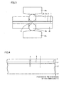
- Fig. 4 is an enlarged cross sectional view of the polymer sheet 1 as used in the present optical switch taken along the optical waveguide 3.
- the optical waveguide 3 is provided lineally in the polymer sheet 1 as a portion having different refractive index from the remainder of the polymer sheet 1.
- the depth to which the optical waveguide 3 is placed is offset to the surface with the notch 4 from the center of thickness of the polymer sheet 1.
- Fig. 5 shows field intensity of an optical signal propagating through an optical waveguide. If the field intensity is sufficiently small at depth L2, the deepest portion of the notch 4 in the optical waveguide, then the total reflection of light can be attained. To this end, a relationship L2-L1>r must be satisfied, where L1 is a depth at the center of the thickness of the waveguide, and r is a mode field radius of the light propagating through the optical waveguide.
- a mode field radius means a radius in which a light intensity distribution in the direction of radius is 1/e 2 (where e is the natural logarithm base: 2.71828%) to the maximum value (usually the value at the center portion of the core of the optical waveguide).
- balls 9a and 9b are employed as direct pushing members in the embodiment described referring to Figs. 2 and 3, a flat pushing member 11 as shown in Fig. 6 may also be employed. Specifically, at least a tip of the member is flat, which is to be pushed against the notch so as to conform to its shape. Thus, the polymer sheet can effectively be deformed.
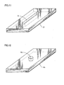
- FIG. 7 is an enlarged view of only one of the ports, while an optical switch in practical use includes multiple array of such ports on a plane. Additionally, one keep plate in contact with the upper surface of a polymer sheet 1 is not shown in Fig. 7.
- a ball 9 is employed also in the present optical switch.
- a keep plate 2e is in contact with bottom of the polymer sheet 1, and a stopper plate 14 is in contact with bottom of the keep plate 2e.
- the keep plate 2e has a tapered hole 17 tapered off upward, and therefrom a slit is extending in two directions forming an angle of approximately 180 ° with each other.
- a stopper plate 14 is provided with a ball receiving hole 18 having a diameter smaller than that of the ball 9.
- the ball 9 is accommodated in the tapered hole 17 and supported by the stopper plate 14 so as to be kept in place.
- the keep plate 2e is arranged relative to the polymer sheet 1 such that the slit 16 conforms to the notch 4.
- the diameter of the ball receiving hole 18 defines maximum downward travel of the ball 9, thereby the ball 9 at its lowest position partially protrudes out of the bottom surface of the stopper plate 14.
- the taper angle and inner diameter of the tapered hole 17 define the maximum upward travel of the ball 9, whereby the ball 9 at its highest position partially protrudes out of the upper surface of the keep plate 2e.
- a piezoelectric actuator 15 is arranged under the stopper plate 14. By the upward and downward displacement of the upper end of the piezoelectric actuator 15, the ball 9 can be displaced upward and downward. As described for the first embodiment, the upward and downward displacement of the ball 9 of the present embodiment deforms the polymer sheet 1 to separate and contact the optical waveguides.
- the travel of the ball 9 in the direction perpendicular to the plane of the polymer sheet 1 (the upward and downward direction) is precisely defined by the keep plate 2e and the stopper plate 14, thus the ball 9 is ensured to be pushed up to a prescribed level regardless of variation in the displacement of the piezoelectric actuator 15. Therefore, a stable performance as an optical switch can be attained.
- pushing mechanism arranged under the polymer sheet is shown in Fig. 7, similar pushing mechanism may be provided at the opposite side (above the polymer sheet) correspondingly.
- FIG. 10 is an enlarged view of only one of the ports, while an optical switch in practical use includes multiple array of such ports on a plane. Additionally, one keep plate in contact with the upper surface of a polymer sheet 1 is not shown in Fig. 10.
- a ball 9 is also employed in the present optical switch.
- a keep plate 2f is in contact with bottom of the polymer sheet 1, and a stopper plate 14n is in contact with bottom of the keep plate 2f.
- the keep plate 2f has a tapered slit 19 tapered off upward.
- a stopper plate 14n is provided with a ball receiving hole 18n in which a straight portion having a diameter slightly larger than that of the ball 9 and a tapered portion tapered off downward are connected.
- the ball 9 is accommodated in a space, supported by the tapered slit 19 and the ball receiving hole 18n.
- the keep plate 2f is arranged relative to the polymer sheet 1 such that the tapered slit 19 conforms to the notch 4.
- the tapered portion of the ball receiving hole 18n defines maximum downward travel of the ball 9, whereby the ball 9 at its lowest position partially protrudes out of the bottom surface of the stopper plate 14n.
- the taper angle of the tapered slit 19 defines the maximum upward travel of the ball 9 being pushed, whereby the ball 9 at its highest position partially protrudes out of the upper surface of the keep plate 2f.
- a piezoelectric actuator 15 is arranged below the stopper plate 14n. By the upward and downward displacement of the upper end of the piezoelectric actuator 15, the ball 9 can be displaced upward and downward. As described for the first embodiment, the upward and downward displacements of the ball 9 of the present embodiment deform the polymer sheet 1 to separate and contact the optical waveguides.
- the travel of the ball 9 in the direction perpendicular to the plane of the polymer sheet 1 is precisely defined by the keep plate 2f and the stopper plate 14n, thus the ball 9 is ensured to be pushed up to a prescribed level regardless of variation in the displacement of the piezoelectric actuator 15. Therefore, a stable performance as an optical switch can be attained. Additionally, the structure of the hole is simpler than the structure described in the second embodiment, thereby the manufacture of the optical switch can be facilitated.
- pushing mechanism under the polymer sheet is shown in Fig. 10, similar pushing mechanism may be provided at the opposite side (above the polymer sheet) correspondingly.
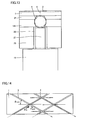
- a reinforce plate 22 having a perforate hole 20 is arranged under the stopper plate 14n.
- the piezoelectric actuator 15 below the reinforce plate 22 pushes up the ball 9 via a bar-like intervening pushing member 21.
- the ball 9 may directly be pushed upward by the piezoelectric actuator 15 without using the bar-like intervening pushing member 21 as shown in Fig 13, even when the reinforce plate 22 is employed.
- the diameter of the perforate hole 20 must be larger than that of the piezoelectric actuator 15 to bring the piezoelectric actuator 15 into contact with the ball 9, which in turn diminishes the effect of the reinforce plate 22. Therefore, when using the reinforce plate 22, the bar-like or pin-like intervening pushing member 21 is preferably employed.
- Fig. 1 referred in the description of the first embodiment, one example of an optical switch is shown, in which at the intersection of two optical waveguides 3 perpendicular to each other, the notch 4 is provided to form an angle of 45° with each optical waveguide 3.
- the angle is not necessarily be 45°, and may be at least of 40° and at most the total reflection angle as shown in Fig. 14.
- the total reflection angle is determined by the refractive index of the optical waveguides 3 and that of the air, which is 48° in the present example.
- an angle ⁇ cut, formed by an optical waveguide 3 and a notch 4 is smaller than the total reflection angle of 48°, then an switching operation can be attained by opening/closing of the notch 4.
- Fig. 15 shows the relationship between the angle ⁇ cut and the reflection Pout/Pin when the notch 4 is closed to contact the optical waveguides 3 with each other.
- a method of manufacturing an optical switch will be described in a fifth embodiment according to the present invention. Particularly, of all the steps included in the manufacturing method, the step of forming a notch 4 in a polymer sheet 1 will be described.
- a cutter 23 is heated by a heater 24 to approximately 300 °C, which is the upper limit of thermally resistant temperature of a polyimide material constituting the polymer sheet 1.
- the cutter 23 is smoothly slid along the polymer sheet 1 to cut the same. Portions to be cut in the polymer sheet 1 are firstly heated by the cutter 23 to weaken the binding of molecules, and thus subsequent contact of the cutter 23 to the polymer sheet 1 facilitates disconnection of the weakened binding of molecules. Accordingly, sections of the polymer sheet are formed smoothly along the sequence of the molecule.
- the section of the notch 4 smoothly formed as described above can achieve decreased optical loss.
- Another method of manufacturing an optical switch will be described in a sixth embodiment. Particularly, of all the steps included in the manufacturing method, the step of forming a notch 4 in a polymer sheet will be described.
- a cutter 23 vibrated with a ultrasound vibrator 23 is employed.
- the cutter 23 is smoothly slid along the polymer sheet 1 to cut the same.
- frictional heat will be generated by the abrasion of the vibrating cutter 23 and the polymer sheet 1.
- Portions to be cut in the polymer sheet 1 are firstly heated by the frictional heat to weaken the binding of molecules, and thus subsequent contact of the cutter 23 to the polymer sheet 1 facilitates disconnection of the weakened binding of molecules. Accordingly, sections of the polymer sheet is formed smoothly along the sequence of the molecule.
- the section of the notch 4 smoothly formed as described above can achieve decreased optical loss. Further, usage of frictional heat as compared to that of heater allows concentrated heat application to the portion of the polymer sheet 1 where cutting is desired. As such, entire deformation of the polymer sheet 1 by the heat is prevented in achieving the object.
- the ultrasound vibrator as means for applying vibration, frictional heat can be generated while the position of the section is precisely controlled.
- the notch can be opened and closed more precisely with small pushing force and small displacement. Therefore, the optical loss is decreased and desired switching operation is ensured.
Landscapes
- Physics & Mathematics (AREA)
- General Physics & Mathematics (AREA)
- Optics & Photonics (AREA)
- Engineering & Computer Science (AREA)
- Microelectronics & Electronic Packaging (AREA)
- Mechanical Light Control Or Optical Switches (AREA)
- Optical Integrated Circuits (AREA)
Applications Claiming Priority (2)
| Application Number | Priority Date | Filing Date | Title |
|---|---|---|---|
| JP2002071959A JP3973458B2 (ja) | 2002-03-15 | 2002-03-15 | 光スイッチ |
| JP2002071959 | 2002-03-15 |
Publications (2)
| Publication Number | Publication Date |
|---|---|
| EP1351078A1 true EP1351078A1 (de) | 2003-10-08 |
| EP1351078B1 EP1351078B1 (de) | 2005-06-01 |
Family
ID=28035143
Family Applications (1)
| Application Number | Title | Priority Date | Filing Date |
|---|---|---|---|
| EP03003958A Expired - Lifetime EP1351078B1 (de) | 2002-03-15 | 2003-02-21 | Optische Schalter und dessen Herstellungsmethode |
Country Status (4)
| Country | Link |
|---|---|
| US (1) | US6873754B2 (de) |
| EP (1) | EP1351078B1 (de) |
| JP (1) | JP3973458B2 (de) |
| DE (1) | DE60300741T2 (de) |
Families Citing this family (3)
| Publication number | Priority date | Publication date | Assignee | Title |
|---|---|---|---|---|
| JP3973458B2 (ja) * | 2002-03-15 | 2007-09-12 | 三菱電機株式会社 | 光スイッチ |
| JP4201645B2 (ja) * | 2003-05-30 | 2008-12-24 | 三菱電機株式会社 | 光スイッチおよびその製造方法 |
| US8559774B2 (en) | 2011-03-31 | 2013-10-15 | Harris Corporation | Optical device having an elastomeric waveguide switch body and related methods |
Citations (6)
| Publication number | Priority date | Publication date | Assignee | Title |
|---|---|---|---|---|
| US4630883A (en) * | 1983-03-21 | 1986-12-23 | The United States Of America As Represented By The Secretary Of The Navy | Optical waveguide apparatus and method for manufacturing |
| GB2200764A (en) * | 1987-01-30 | 1988-08-10 | Stc Plc | N-way redundant optical fibre switch |
| EP0935149A2 (de) * | 1998-02-04 | 1999-08-11 | Hewlett-Packard Company | Elément de commutation avec guide d'onde à coeur élargi |
| WO2001073481A2 (en) * | 2000-03-30 | 2001-10-04 | K2 Optronics, Inc. | Optical routing element for use in fiber optic systems |
| US20020067878A1 (en) * | 2000-12-06 | 2002-06-06 | Mitsubishi Denki Kabushiki Kaisha | Optical switch and method of producing the same |
| US20020168133A1 (en) * | 2001-05-09 | 2002-11-14 | Mitsubishi Denki Kabushiki Kaisha | Optical switch and optical waveguide apparatus |
Family Cites Families (13)
| Publication number | Priority date | Publication date | Assignee | Title |
|---|---|---|---|---|
| US4365862A (en) * | 1980-01-18 | 1982-12-28 | Nippon Telegraph & Telephone Public Corporation | Optical switch |
| JPS57163205A (en) | 1981-03-31 | 1982-10-07 | Matsushita Electric Works Ltd | Optical switch |
| JPS60222816A (ja) | 1984-04-20 | 1985-11-07 | Hitachi Ltd | 光電的接点 |
| JPH02136805A (ja) | 1988-11-18 | 1990-05-25 | Nippon Sheet Glass Co Ltd | 導波型光電子マトリックススイッチ |
| JPH05196973A (ja) * | 1991-09-12 | 1993-08-06 | Sumitomo Electric Ind Ltd | 光スイッチ |
| JPH05289006A (ja) | 1992-04-13 | 1993-11-05 | Fujikura Ltd | 光路切替装置 |
| JPH07294748A (ja) | 1994-04-20 | 1995-11-10 | Mitsubishi Rayon Co Ltd | プラスチック光ファイバ切断法 |
| JP3429196B2 (ja) | 1998-05-29 | 2003-07-22 | 日本電信電話株式会社 | ポリマ導波路光スイッチの組立方法 |
| US6611635B1 (en) * | 1998-10-09 | 2003-08-26 | Fujitsu Limited | Opto-electronic substrates with electrical and optical interconnections and methods for making |
| US6507682B2 (en) * | 2001-04-06 | 2003-01-14 | Ngk Insulators, Ltd. | Optical switch |
| JP4471545B2 (ja) * | 2001-09-03 | 2010-06-02 | 三菱電機株式会社 | 光スイッチ |
| JP3986840B2 (ja) * | 2002-02-01 | 2007-10-03 | 三菱電機株式会社 | 光スイッチの製造方法 |
| JP3973458B2 (ja) * | 2002-03-15 | 2007-09-12 | 三菱電機株式会社 | 光スイッチ |
-
2002
- 2002-03-15 JP JP2002071959A patent/JP3973458B2/ja not_active Expired - Fee Related
- 2002-09-18 US US10/245,638 patent/US6873754B2/en not_active Expired - Fee Related
-
2003
- 2003-02-21 EP EP03003958A patent/EP1351078B1/de not_active Expired - Lifetime
- 2003-02-21 DE DE60300741T patent/DE60300741T2/de not_active Expired - Fee Related
Patent Citations (6)
| Publication number | Priority date | Publication date | Assignee | Title |
|---|---|---|---|---|
| US4630883A (en) * | 1983-03-21 | 1986-12-23 | The United States Of America As Represented By The Secretary Of The Navy | Optical waveguide apparatus and method for manufacturing |
| GB2200764A (en) * | 1987-01-30 | 1988-08-10 | Stc Plc | N-way redundant optical fibre switch |
| EP0935149A2 (de) * | 1998-02-04 | 1999-08-11 | Hewlett-Packard Company | Elément de commutation avec guide d'onde à coeur élargi |
| WO2001073481A2 (en) * | 2000-03-30 | 2001-10-04 | K2 Optronics, Inc. | Optical routing element for use in fiber optic systems |
| US20020067878A1 (en) * | 2000-12-06 | 2002-06-06 | Mitsubishi Denki Kabushiki Kaisha | Optical switch and method of producing the same |
| US20020168133A1 (en) * | 2001-05-09 | 2002-11-14 | Mitsubishi Denki Kabushiki Kaisha | Optical switch and optical waveguide apparatus |
Also Published As
| Publication number | Publication date |
|---|---|
| US6873754B2 (en) | 2005-03-29 |
| JP3973458B2 (ja) | 2007-09-12 |
| EP1351078B1 (de) | 2005-06-01 |
| DE60300741T2 (de) | 2006-03-23 |
| DE60300741D1 (de) | 2005-07-07 |
| JP2003270561A (ja) | 2003-09-25 |
| US20030174927A1 (en) | 2003-09-18 |
Similar Documents
| Publication | Publication Date | Title |
|---|---|---|
| JPH11287962A (ja) | スイッチング素子 | |
| US6163643A (en) | Micro-mechanical variable optical attenuator | |
| US6922508B2 (en) | Optical switching apparatus with adiabatic coupling to optical fiber | |
| EP0887673B1 (de) | Selbstausgerichteter mechanischer MxN optischer Schalter | |
| US5481629A (en) | Hybrid optical IC with optical axes at different levels | |
| WO2001063351A1 (en) | Acousto-optical switch for fiber optic lines | |
| US6915029B2 (en) | High density integrated optical chip with low index difference and high index difference waveguide functions | |
| US7043111B2 (en) | Optical parts coupling structure, method of manufacturing the same, optical switch, two-dimensional lens array, and method of manufacturing the same | |
| JP2004078195A (ja) | 導波路内を伝播する光信号の経路を変更する方法、光スイッチング装置、光信号を第1の導波路から第2の導波路に切り替える方法、光信号を導波路から送り出すシステム、及び三次元多層光スイッチ | |
| CN101821654B (zh) | 光信号在光学装置之间的有效传送 | |
| EP1351078B1 (de) | Optische Schalter und dessen Herstellungsmethode | |
| US6510259B1 (en) | Optical switch using an integrated Mach-Zehnder interferometer having a movable phase shifter and asymmetric arms | |
| US6404941B1 (en) | Optical multiple circuit breaker | |
| US6804427B2 (en) | Optical switch | |
| US6445845B1 (en) | Optical switch | |
| US6519381B2 (en) | Optical switch and method of producing the same | |
| US6529653B1 (en) | System and method for orienting and positioning optical fibers | |
| US6563965B1 (en) | Analog optical switch using an integrated Mach-Zehnder interferometer having a moveable phase shifter | |
| JP2000193838A (ja) | 光導波路構造体 | |
| US6778726B2 (en) | Optical switch | |
| US6847756B2 (en) | Optical switching matrix and method of fabricating such a matrix | |
| WO2001059492A2 (en) | Optical waveguide and shutter | |
| US20030095749A1 (en) | Fiber coupler and compensation system | |
| US6829402B2 (en) | Optical switch and method of manufacturing the same | |
| US20030012494A1 (en) | Compact optical beam separator and method |
Legal Events
| Date | Code | Title | Description |
|---|---|---|---|
| PUAI | Public reference made under article 153(3) epc to a published international application that has entered the european phase |
Free format text: ORIGINAL CODE: 0009012 |
|
| 17P | Request for examination filed |
Effective date: 20030708 |
|
| AK | Designated contracting states |
Kind code of ref document: A1 Designated state(s): AT BE BG CH CY CZ DE DK EE ES FI FR GB GR HU IE IT LI LU MC NL PT SE SI SK TR |
|
| AX | Request for extension of the european patent |
Extension state: AL LT LV MK RO |
|
| 17Q | First examination report despatched |
Effective date: 20031222 |
|
| AKX | Designation fees paid |
Designated state(s): DE FR GB IT |
|
| GRAP | Despatch of communication of intention to grant a patent |
Free format text: ORIGINAL CODE: EPIDOSNIGR1 |
|
| GRAS | Grant fee paid |
Free format text: ORIGINAL CODE: EPIDOSNIGR3 |
|
| GRAA | (expected) grant |
Free format text: ORIGINAL CODE: 0009210 |
|
| AK | Designated contracting states |
Kind code of ref document: B1 Designated state(s): DE FR GB IT |
|
| REG | Reference to a national code |
Ref country code: GB Ref legal event code: FG4D |
|
| REF | Corresponds to: |
Ref document number: 60300741 Country of ref document: DE Date of ref document: 20050707 Kind code of ref document: P |
|
| REG | Reference to a national code |
Ref country code: GB Ref legal event code: 727 |
|
| REG | Reference to a national code |
Ref country code: GB Ref legal event code: 727A |
|
| REG | Reference to a national code |
Ref country code: GB Ref legal event code: 727H |
|
| ET | Fr: translation filed | ||
| PLBE | No opposition filed within time limit |
Free format text: ORIGINAL CODE: 0009261 |
|
| STAA | Information on the status of an ep patent application or granted ep patent |
Free format text: STATUS: NO OPPOSITION FILED WITHIN TIME LIMIT |
|
| RAP2 | Party data changed (patent owner data changed or rights of a patent transferred) |
Owner name: MITSUBISHI DENKI KABUSHIKI KAISHA |
|
| 26N | No opposition filed |
Effective date: 20060302 |
|
| PGFP | Annual fee paid to national office [announced via postgrant information from national office to epo] |
Ref country code: DE Payment date: 20070215 Year of fee payment: 5 |
|
| PGFP | Annual fee paid to national office [announced via postgrant information from national office to epo] |
Ref country code: GB Payment date: 20070221 Year of fee payment: 5 |
|
| REG | Reference to a national code |
Ref country code: GB Ref legal event code: 746 Effective date: 20070417 |
|
| PGFP | Annual fee paid to national office [announced via postgrant information from national office to epo] |
Ref country code: IT Payment date: 20070526 Year of fee payment: 5 |
|
| PGFP | Annual fee paid to national office [announced via postgrant information from national office to epo] |
Ref country code: FR Payment date: 20070208 Year of fee payment: 5 |
|
| GBPC | Gb: european patent ceased through non-payment of renewal fee |
Effective date: 20080221 |
|
| REG | Reference to a national code |
Ref country code: FR Ref legal event code: ST Effective date: 20081031 |
|
| PG25 | Lapsed in a contracting state [announced via postgrant information from national office to epo] |
Ref country code: DE Free format text: LAPSE BECAUSE OF NON-PAYMENT OF DUE FEES Effective date: 20080902 |
|
| PG25 | Lapsed in a contracting state [announced via postgrant information from national office to epo] |
Ref country code: FR Free format text: LAPSE BECAUSE OF NON-PAYMENT OF DUE FEES Effective date: 20080229 |
|
| PG25 | Lapsed in a contracting state [announced via postgrant information from national office to epo] |
Ref country code: GB Free format text: LAPSE BECAUSE OF NON-PAYMENT OF DUE FEES Effective date: 20080221 |
|
| PG25 | Lapsed in a contracting state [announced via postgrant information from national office to epo] |
Ref country code: IT Free format text: LAPSE BECAUSE OF NON-PAYMENT OF DUE FEES Effective date: 20080221 |