EP1351272A2 - Verfahren und Gerät zur Elektronenstrahlbelichtung und Verfahren zur Herstellung von Vorrichtungen mittels einem solchen Gerät - Google Patents
Verfahren und Gerät zur Elektronenstrahlbelichtung und Verfahren zur Herstellung von Vorrichtungen mittels einem solchen Gerät Download PDFInfo
- Publication number
- EP1351272A2 EP1351272A2 EP02017787A EP02017787A EP1351272A2 EP 1351272 A2 EP1351272 A2 EP 1351272A2 EP 02017787 A EP02017787 A EP 02017787A EP 02017787 A EP02017787 A EP 02017787A EP 1351272 A2 EP1351272 A2 EP 1351272A2
- Authority
- EP
- European Patent Office
- Prior art keywords
- pattern
- electron
- shift amount
- electron beams
- deflection
- Prior art date
- Legal status (The legal status is an assumption and is not a legal conclusion. Google has not performed a legal analysis and makes no representation as to the accuracy of the status listed.)
- Granted
Links
Images


Classifications
-
- H—ELECTRICITY
- H01—ELECTRIC ELEMENTS
- H01J—ELECTRIC DISCHARGE TUBES OR DISCHARGE LAMPS
- H01J37/00—Discharge tubes with provision for introducing objects or material to be exposed to the discharge, e.g. for the purpose of examination or processing thereof
- H01J37/30—Electron-beam or ion-beam tubes for localised treatment of objects
- H01J37/302—Controlling tubes by external information, e.g. program control
- H01J37/3023—Program control
- H01J37/3026—Patterning strategy
-
- B—PERFORMING OPERATIONS; TRANSPORTING
- B82—NANOTECHNOLOGY
- B82Y—SPECIFIC USES OR APPLICATIONS OF NANOSTRUCTURES; MEASUREMENT OR ANALYSIS OF NANOSTRUCTURES; MANUFACTURE OR TREATMENT OF NANOSTRUCTURES
- B82Y10/00—Nanotechnology for information processing, storage or transmission, e.g. quantum computing or single electron logic
-
- B—PERFORMING OPERATIONS; TRANSPORTING
- B82—NANOTECHNOLOGY
- B82Y—SPECIFIC USES OR APPLICATIONS OF NANOSTRUCTURES; MEASUREMENT OR ANALYSIS OF NANOSTRUCTURES; MANUFACTURE OR TREATMENT OF NANOSTRUCTURES
- B82Y40/00—Manufacture or treatment of nanostructures
-
- H—ELECTRICITY
- H01—ELECTRIC ELEMENTS
- H01J—ELECTRIC DISCHARGE TUBES OR DISCHARGE LAMPS
- H01J37/00—Discharge tubes with provision for introducing objects or material to be exposed to the discharge, e.g. for the purpose of examination or processing thereof
- H01J37/30—Electron-beam or ion-beam tubes for localised treatment of objects
- H01J37/304—Controlling tubes by information coming from the objects or from the beam, e.g. correction signals
-
- H—ELECTRICITY
- H01—ELECTRIC ELEMENTS
- H01J—ELECTRIC DISCHARGE TUBES OR DISCHARGE LAMPS
- H01J37/00—Discharge tubes with provision for introducing objects or material to be exposed to the discharge, e.g. for the purpose of examination or processing thereof
- H01J37/30—Electron-beam or ion-beam tubes for localised treatment of objects
- H01J37/317—Electron-beam or ion-beam tubes for localised treatment of objects for changing properties of the objects or for applying thin layers thereon, e.g. for ion implantation
- H01J37/3174—Particle-beam lithography, e.g. electron beam lithography
- H01J37/3177—Multi-beam, e.g. fly's eye, comb probe
Definitions
- the present invention relates to an electron beam exposure technique used for processing and exposing a semiconductor integrated circuit or the like.
- the invention has been achieved in consideration of the problems and its object is to provide a high-precision and high-speed electron beam exposure technique capable of correcting the position of each beam with a simple configuration in a multi-beam exposure system.
- the means for computing the positional shift amount of the pattern is constructed by means for performing pattern data linear interpolation, and the apparatus includes irradiation amount control means for converting the result of the linear interpolation to an irradiation amount.
- Exposure is made by moving the specimen 217 mounted on the specimen stage 218.
- Reference numeral 219 denotes a Faraday cup which is mounted on the specimen stage and has knife edges in the X and Y directions.
- the Faraday cup 219 measures a charge amount synchronously with deflection of an electron beam on the specimen or movement of the Faraday cup 219 interlocking with the stage control circuit 225 including a coordinate measuring function (not shown) such as a laser interferometer, thereby enabling the position of the electron beam to be measured on the specimen, which forms the intermediate images.
- the position of an electron beam can be measured also by a method of attaching a mark 227 for position measurement onto the specimen stage, scanning the mark 227, detecting a signal of an electron detector 216, and processing the signal by a signal processing circuit 224. On the basis of the measured beam position, a shift amount of each beam is computed.
- the pitches of the openings in the aperture array 204, lens array 205, blanking array 207, and blanking aperture 208 are almost the same.
- the pitch in the specimen is 4 ⁇ m and the magnification of the projection optical system is 1/50, the pitch is 200 ⁇ m.
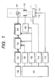
- a shift amount is computed by a shift computing circuit constructed by the bit map memory 103, a bit map shifting circuit 104, and a shift amount control circuit 105.
- the pattern data of each bit map memory 103 is shifted by the bit map shifting circuit 104.
- Parameters such as a shift amount are set from the shift amount control circuit 105.
- a value obtained by the shift computation is converted to a blanking-off time signal by an irradiation amount control circuit 106, and the signal is supplied to each blanking electrode in a blanking array 107.
- the bit map shift computation and the irradiation amount control are performed in parallel by an amount corresponding to the number of beams in the sub field synchronously with a sync signal from a deflection signal generating circuit 108.
- the sync signal is also input to a deflection control circuit 109, and is also synchronized with an output of the deflection control circuit 109 and a deflection signal supplied to a deflector 110.
- the pattern data shifted is written in the area including the deflection area margin by a single deflector 110.
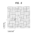
- FIG. 5 shows a bit map memory in a micro field.
- the i-th data in the x-direction and the j-th data in the y-direction stored in the memory is referred to as f(i, j).
- the shift smaller than a pixel is performed by using linear interpolation computation.
- the linear interpolation is expressed by the following equation.
- the shift in the y-direction is similarly as follows.
- f(i,j) (1 - dy)f(i,j) + dyf(i,j-1)
- Shifts in both of the x and y directions are computed by computing the shift in each of the x- and y-directions.
- the above computation is carried out by reading of data from the bit map memory, addition, and multiplication.
- a computing circuit such as a general microprocessor having a calculation program is used.
- a dedicated circuit has to be constructed.
- FIG. 12 shows an example of the circuit configuration.
- f(i,j) read from the bit map memory is supplied to a shift register 1201 and also subjected to sign change and supplied to an adder 1202.
- the shift register holds the immediately preceding data. It is assumed here that beam deflection in the micro field corresponds to the increase direction of x, that is, increment of "i".
- the output of the shift register 1201 is also input to the adder 1201 and, f(i-1,j) - f(i,j) is output as a result.
- the output is multiplied by dx by a multiplexer 1203.
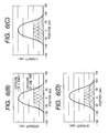
- FIGS. 6(A) to 6(D) show beam profiles as the result of shifting of the data.
- FIG. 6(B) shows an example of forming a pattern of 100 nm by irradiating five pixels of 20 nm with a beam having a beam blur of 20 nm.
- FIGS. 6(A) to 6(D) show only one-dimensional direction for simplicity of explanation, the case of two-dimensional direction is substantially the same.
- the beam irradiation amount at the left end becomes 80% of the original irradiation amount, and the sixth pixel from the right end is irradiated with a 20% irradiation amount.
- the pattern of 100 nm is shifted by 4 nm.
- the beam irradiation amount at both ends becomes 50%.
- FIG. 6(A) shows those shifts of the pattern of 100 nm.
- the shift equal to or larger than a pixel is realized by changing the reading position in a bit map memory. It is sufficient to add an offset to each of "i" and "j" in f(i,j).
- f'(i,j) f(i+i offset ,j+j offset ) where f' denotes an irradiation amount in an exposed pixel position, i offset denotes a reading position offset in the x-direction, and j offset denotes a reading position offset in the y-direction.
- the direction of a shift can be changed.
- the pattern can be shifted only in the positive direction (the direction in which coordinates increase) in each of the x- and y-directions.
- the reading position offset is -2 and the shift amount smaller than the pixel is 5 nm.
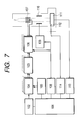
- the order of the bit map memory 103 and the bit map shifting circuit 104 constructing the shift amount computing circuit is different from that of FIG. 1.
- Exposure pattern data stored in the CPU 101 is developed to bit map data in a pixel unit by the bit map developing circuit 102.
- the developed data is divided on a micro field unit basis.
- the divided data is shifted by the bit map shifting circuit 104 every micro field.
- the resultant data is stored as irradiation amount data in the bit map memory 103 constructed by the number of micro fields.
- the bit-map memory 103 is read by the irradiation amount control circuit 106 synchronously with deflection and converted into a blanking-off time signal.
- the blanking-off time signal is supplied to each of the blanking electrodes of the blanking array 107.
- the other configuration is similar to that of FIG. 1.
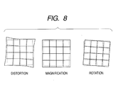
- FIG. 8 shows the distortion, magnification error, and rotation error among the aberrations.
- Broken lines in the diagram show ideal lattices, and solid lines indicate deviations from the ideal lattices.
- the aberrations correspond to shifts of each beam position. By shifting the exposure position, the aberrations can be corrected.
- a shift amount has to be computed every deflecting operation.
- an aberration caused by deflection has dependency on position in the plane-shaped beam (sub field) depending on the main deflection amount.
- the shape of the micro field also has dependency on the main deflection amount and position in the sub field depending on the main deflection amount.
- the position dependency can be approximated by a cubic polynomial of a deflection distance in theory. Therefore, a correction amount in a micro field can be calculated by the following equations. where dx and dy denote correction amounts depending on positions x ⁇ and y ⁇ in the micro field.
- Ten coefficients from a 00 to a 33 and ten coefficients from b 00 to b 33 depend on main deflection amounts x m and y m and positions x s and y s in a sub field. For example, when a 00 depends on the position x s , y s in the sub field and the coefficients in this case are c 00 to c 33 , it is expressed as the following Equation 7 in a manner similar to Equation 6.
- Equation 3 The coefficients other than the coefficients a 00 and c 00 are similar to those in Equation 6.
- the coefficient "b" can be also similarly obtained. Therefore, dx and dy in Equation 3 are values depending on the deflection position and are expressed as dx(i,j) and dy(i,j), respectively.
- the position dependency of the shift amount that is, the coefficients of "a” and "b” in Equation 6 can be obtained by determining a few to tens of representative positions and measuring a beam position with respect to all of the deflection amounts as described above, or by performing a trial exposure, measuring a shift amount from a design position, and executing least square approximation or the like.
- FIG. 9 shows the configuration of exposure control. Since the configuration is similar to that of FIG. 1, it will be described by using the same reference numerals. Shifting of pattern data depends on deflection coordinates, so that computation of Equation 6 has to be performed synchronously with deflection. Therefore, synchronously with a sync signal from a deflection signal generating circuit 108, a main deflection amount and a shift amount depending on a position in a sub field are computed by a shift amount control circuit 105 as a component of the shift amount computing circuit. Further, a shift amount of pattern data is actually computed by a bit map shift circuit 104. The subsequent operations are the same as those in the example shown in FIG. 1.
- an aberration can be reduced to a degree that it can be ignored in comparison with required precision.
- dependency on the deflection amount of correction computation can be decreased, and a simplified deflection amount can be used.
- X ⁇ and Y ⁇ are set to only rotation and magnification (they are used only for the term of the first degree), and a case where dependency of X ⁇ and Y ⁇ is not considered.
- the deflection amount dependency of coefficients of "a" and "b” in Equation 6 may be expressed as X m +X s +X ⁇ and Y m +Y s +Y ⁇ , or X m +X s and Y m +Y s .
- a distortion of a sub field of a 256 ⁇ m square can be reduced to about 100 nm at an end portion of a main field of 4 mm.
- deformation of a micro field of a 4 ⁇ m square becomes about 1 nm at the maximum and can be ignored. That is, it becomes unnecessary to compute dependency of X ⁇ and Y ⁇ .
- a deviation occurs in relative positional relation between a micro field in the center of a sub field and a micro field in an end portion of the sub field and, as a result, a deviation occurs in connection with neighboring sub fields.
- the main deflection amount and the shift terms (aoo and boo in Equation 6) depending on the main deflection amount and the position in the sub field are computed in each micro field. Based on the computation, exposure is performed while shifting the center position of each micro field. As a result, a connection error of micro fields can be decreased to an ignorable degree.
- n denotes the number assigned to each beam (in the case of 1000 beams, the numbers are from 1 to 1000). Since dependency on position in a sub field is not considered, a coefficient "a" depends on only the main deflection amounts x m and y n , . where n corresponds to n in Equation 9. A coefficient is computed by a method of measuring dependency on the main deflection amount of each of all the beams.
- the beams are deflected in some positions at a proper interval (for example, the size of a sub field), and the position of each beam in the position is obtained by mark detection or the like.
- the positions are approximated by a polynomial (Equation 10), the value of the coefficient "a" of each beam can be computed.
- the coefficient "b" can be also similarly calculated.
- a strain in a sub field of 256 ⁇ m ⁇ 256 ⁇ m is about 100 nm in an end portion of a main field of 4 mm and deformation of a micro field of a 4 ⁇ m square is about 1 nm at the maximum, it is unnecessary to compute dependency of X ⁇ and Y ⁇ .
- To obtain a deviation in a relative position relation between a micro field in the center of a sub field and a micro field in an end portion of a sub field it is sufficient to compute only a shift term (a 00 and b 00 in Equation 9) depending on the main deflection amount of all of the beams. Only by performing exposure while shifting the center position of each micro field on the basis of the computation, the connection error of micro fields is reduced to an ignorable degree.
- a positional shift of a beam caused by deflection as described usually depends on the deflection amount and increases. That is, a shift amount in the deflection position 0 (on the optical axis) and that in the maximum deflection position are different from each other.
- FIG. 13 (A) shows the shape of a distortion on the center axis.
- FIG. 13 (B) shows the shape of the distortion in a maximum deflection position.
- the hatched area in FIG. 13 (B) indicates the most distorted micro field.
- a micro field 1302 in the maximum deflection position is deformed more than a micro field 1301 in the deflection position 0 and has a larger data shift amount, so that a larger deflection area margin is necessary.
- FIG. 13 (A) shows the shape of a distortion on the center axis.
- FIG. 13 (B) shows the shape of the distortion in a maximum deflection position.
- FIG. 13 (C) shows the relation between a micro field size 1303 in the deflection position 0 and a deflection area margin 1304, and FIG. 13 (D) shows the relation between a micro field size 1305 in the maximum deflection position and a deflection area margin 1306.
- the deflection area margins are one pixel and three pixels, respectively. It is sufficient to set a change in the deflection margin area by setting a set value of a counter for reading a bit map memory so as to depend on the deflection amount.
- the deflection area margin is an area where a beam is actually deflected. If the deflection area margin is small, there is no deflection of an excessive area. Thus, exposure speed is improved.
- a positional shift of a beam caused by deflection as shown depends on the deflecting operation and is always constant.
- a change with time in the position of the electron beam that is, a so-called beam drift cannot be predicted.
- a deflector array for beam position adjustment may be provided for each of a plurality of beams.
- FIG. 14 shows an example where the electron beam exposure apparatus of FIG. 2 is provided with a deflector array for beam position adjustment. Since FIG. 14 is similar to FIG. 2 and the same reference numerals are used, only different points will be described.
- a deflector array 1401 is provided below the blanking aperture 208. Even when the deflector array 1401 is mounted above the blanking aperture 208, an equivalent function can be obtained.
- the deflector array 1401 By the deflector array 1401, a beam interval on a specimen can be corrected. The correction is made by measuring each beam position as described and applying a voltage by an optical axis controller 1402 so as to set the predetermined interval. Since the optical axis which is set once is maintained constant until the next measurement, a high-speed circuit is not necessary for the optical axis controller 1402. In such a state, correction by data shifting depending on the deflection as described is made, thereby enabling the beam positional shift due to a manufacturing error to be eliminated. Thus, the deflection area margin can be efficiently used.
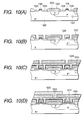
- FIGS. 10 (A) to 10 (D) show a process of fabricating a semiconductor integrated circuit by using an electron beam exposure method of the invention.
- FIGS. 10 (A) to 10 (D) are cross sections of a device fabricated in the process.
- an N - silicon substrate 1020, a p-well layer 1021, a p-layer 1022, a field oxide film 1023, a polysilicon/silicon oxide film gate 1024, a p high-density diffusion layer 1025, an N high-density diffusion layer 1026, and the like are formed by a normal method (FIG. 10(A)).
- an insulating film 1027 made of phosphorus glass is deposited and undergoes dry etching, thereby forming a contact hole 1028 (FIG. 10 (B)).
- an interlayer insulating film 1031 is formed and a hole pattern 1032 is formed by a normal method.
- the hole pattern 1032 is buried with an W plug, and a second wiring 1033 made of Al is connected (FIG. 10 (D)).
- the following passivation process used is a conventional one.
- an electron source of an MIN (metal-insulator-metal) type, an MIS (Metal-Insulator-Semiconductor) type, an FEA (Field Emission Array) type in which needle-shaped chips are arranged, and a type in which carbon nanotubes are arranged can be used.
- an MIS type in which an insulation layer is formed of SiO 2 of 140 ⁇ , and metal layers are formed by Al of 15 ⁇ and Au of 25 ⁇ on the insulating layer is used.
- a voltage of 10V is applied to the metal layer in the structure, electrons pass through the metal layer at a current density of about 1 mA/cm 2 .
- Electron emission occurs when a voltage is applied to the metal layer and emission of the electron beam can be controlled by the voltage.
- the electron emission amount is controlled by the magnitude of an application voltage or time of the voltage application.
- the controls are performed by the irradiation amount control circuit 221 based on pattern data.
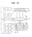
- FIG. 17 shows the example.
- FIG. 17 will be described by using the same reference numerals as those of FIG. 16.
- FIG. 17 is the same as FIG. 16 except that the image of the plane-shaped electron source 1701 is in the position corresponding to the position of the intermediate image 209 shown in FIG. 16 and the lens array and the focus control circuit are not provided.
- the electron source of the FEA type can control the emission of the electron beam and the irradiation amount by controlling a voltage of an extraction electrode. This control is performed by the irradiation amount control circuit 221 on the basis of pattern data.
- FIG. 18 shows the configuration of a controller in the case of using a plane-shaped electron source by using the same reference numerals as those in FIG. 1.
- FIG. 18 is the same as FIG. 1 except that an output from the irradiation amount control circuit 106 is input to, not the blanking array but, a plane-shaped electron source 1801.
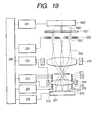
- FIG. 19 shows an example of an electron beam exposure apparatus of a multi-beam type using an optical excitation electron source.
- the exposure apparatus of FIG. 19 is the same as that of FIG. 16 except for means for generating an electron beam and will be described by using the same reference numerals as those of FIG. 16.
- Excitation beams 1902 are emitted from an excitation beam generating apparatus 1903 to the optical excitation electron source 1901 from which the separated electron beams 206 are emitted.
- the configuration after that is the same as that of FIG. 16.
- the optical excitation electron source or so-called photo cathode is fabricated by forming a semiconductor layer and a surface absorption layer on a glass substrate.
- the material of the semiconductor layer is a p-type semiconductor which is a III-V group material such as GaAs, AlAs, InP, InAs, GaP, or GaN, a IV group material such as Si, C, or Ge, or a mixture of them.
- the surface absorption layer is made of an alkali metal such as Cs or Na, the alkali metal such as Cs or Na and oxygen, an alkali earth metal such as Ba and oxygen, or a mixture of them.
- an AlGaAs film having a thickness of 2 ⁇ m and a GaAs film having a thickness of 1.5 ⁇ m are formed on a glass substrate, a few atom layers made of Cs are formed on the GaAs film, and the resultant is used.
- the optical excitation electron source is irradiated with excitation light from the glass substrate face by a laser diode.
- a current of about 25 ⁇ A can be obtained with the excitation light of 1 mW.
- the emission of the electron beam and the emission amount can be controlled by changing emission of the excitation light and intensity of excitation light or irradiation time. The control is performed by the irradiation amount control circuit 221 based on the pattern data.
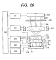
- the optical excitation electron source can achieve a high current density. Consequently, by converging the excitation light by the optical excitation electron source, the configuration which does not use an intermediate image shown in FIG. 20 can be employed.
- FIG. 20 the same reference numerals as those of FIG. 19 are used.
- An excitation beam 2002 generated by an excitation beam generating apparatus 2003 is converged and is emitted to an optical excitation electron source 2001.
- the following configuration from the electron beam 206 emitted and separated is the same as FIG. 19.
- FIG. 21 shows the configuration of a control apparatus in the case of using the optical excitation electron source.
- the same reference numerals as those of FIG. 18 are used.
- FIG. 21 is the same as FIG. 18 except that an output from the irradiation amount control circuit 106 is input to not the blanking array but an optical excitation light generating apparatus 2102 and the generated excitation light is emitted to an optical excitation electron source 2101.
- control apparatuses shown in FIGS. 18 and 21 As the control apparatuses shown in FIGS. 18 and 21, the control apparatuses shown in FIGS. 7 and 9 can be also applied.
- an electron beam exposure method for forming a desired pattern onto a specimen by independently emitting and scanning a plurality of electron beams, wherein a deviation between a pattern formed by each of the plurality of electron beams and the desired pattern is controlled by shifting the position of pattern data of the pattern formed by each of the plurality of electron beams.
- high-precision and high-speed exposure can be performed with a simple configuration in a multi-beam type electron beam exposure method and apparatus.
Landscapes
- Chemical & Material Sciences (AREA)
- Engineering & Computer Science (AREA)
- Nanotechnology (AREA)
- Analytical Chemistry (AREA)
- Physics & Mathematics (AREA)
- Crystallography & Structural Chemistry (AREA)
- Condensed Matter Physics & Semiconductors (AREA)
- General Physics & Mathematics (AREA)
- Manufacturing & Machinery (AREA)
- Mathematical Physics (AREA)
- Theoretical Computer Science (AREA)
- Electron Beam Exposure (AREA)
Applications Claiming Priority (2)
| Application Number | Priority Date | Filing Date | Title |
|---|---|---|---|
| JP2002102789 | 2002-04-04 | ||
| JP2002102789A JP3940310B2 (ja) | 2002-04-04 | 2002-04-04 | 電子ビーム描画方法及び描画装置、並びにこれを用いた半導体製造方法 |
Publications (3)
| Publication Number | Publication Date |
|---|---|
| EP1351272A2 true EP1351272A2 (de) | 2003-10-08 |
| EP1351272A3 EP1351272A3 (de) | 2006-01-04 |
| EP1351272B1 EP1351272B1 (de) | 2017-03-01 |
Family
ID=28035951
Family Applications (1)
| Application Number | Title | Priority Date | Filing Date |
|---|---|---|---|
| EP02017787.9A Expired - Lifetime EP1351272B1 (de) | 2002-04-04 | 2002-08-12 | Elektronenstrahlbelichtungsverfahren |
Country Status (3)
| Country | Link |
|---|---|
| US (1) | US6667486B2 (de) |
| EP (1) | EP1351272B1 (de) |
| JP (1) | JP3940310B2 (de) |
Cited By (2)
| Publication number | Priority date | Publication date | Assignee | Title |
|---|---|---|---|---|
| WO2008044030A1 (en) * | 2006-10-12 | 2008-04-17 | Vistec Lithography Inc | Workpiece height adjustment in an electron beam lithography machine |
| JP2015138882A (ja) * | 2014-01-22 | 2015-07-30 | 株式会社ニューフレアテクノロジー | マルチ荷電粒子ビーム描画装置及びマルチ荷電粒子ビーム描画方法 |
Families Citing this family (39)
| Publication number | Priority date | Publication date | Assignee | Title |
|---|---|---|---|---|
| EP1249855B1 (de) * | 2001-04-09 | 2008-07-09 | ICT Integrated Circuit Testing Gesellschaft für Halbleiterprüftechnik mbH | Vorrichtung und Verfahren zur Kontrolle von fokussierten Elektronenstrahlen |
| JP4109944B2 (ja) * | 2002-09-20 | 2008-07-02 | キヤノン株式会社 | 固体撮像装置の製造方法 |
| ATE538412T1 (de) * | 2002-10-25 | 2012-01-15 | Mapper Lithography Ip Bv | Lithographisches system |
| AU2003276779A1 (en) * | 2002-10-30 | 2004-05-25 | Mapper Lithography Ip B.V. | Electron beam exposure system |
| JP4421836B2 (ja) * | 2003-03-28 | 2010-02-24 | キヤノン株式会社 | 露光装置及びデバイス製造方法 |
| CN101103417B (zh) | 2003-09-05 | 2012-06-27 | 卡尔蔡司Smt有限责任公司 | 粒子光学系统和排布结构,以及用于其的粒子光学组件 |
| GB2408143B (en) * | 2003-10-20 | 2006-11-15 | Ims Nanofabrication Gmbh | Charged-particle multi-beam exposure apparatus |
| JP2005276869A (ja) * | 2004-03-23 | 2005-10-06 | Jeol Ltd | 荷電粒子ビーム描画装置。 |
| JP4477436B2 (ja) * | 2004-06-30 | 2010-06-09 | キヤノン株式会社 | 荷電粒子線露光装置 |
| JP2006113429A (ja) * | 2004-10-18 | 2006-04-27 | Toppan Printing Co Ltd | レリーフパターンの作製方法およびレリーフパターン |
| DE102004055149B4 (de) * | 2004-11-16 | 2007-07-19 | Leica Microsystems Lithography Gmbh | Vorrichtung und Verfahren zum Abbilden eines Mehrfach-Partikelstrahls auf ein Substrat |
| US7576341B2 (en) * | 2004-12-08 | 2009-08-18 | Samsung Electronics Co., Ltd. | Lithography systems and methods for operating the same |
| US20090212213A1 (en) * | 2005-03-03 | 2009-08-27 | Ebara Corporation | Projection electron beam apparatus and defect inspection system using the apparatus |
| WO2006101116A1 (ja) * | 2005-03-22 | 2006-09-28 | Ebara Corporation | 電子線装置 |
| US8067732B2 (en) * | 2005-07-26 | 2011-11-29 | Ebara Corporation | Electron beam apparatus |
| JP4795755B2 (ja) * | 2005-08-25 | 2011-10-19 | 株式会社日立ハイテクノロジーズ | 半導体基板の製造装置 |
| EP1760762B1 (de) * | 2005-09-06 | 2012-02-01 | ICT Integrated Circuit Testing Gesellschaft für Halbleiterprüftechnik mbH | Vorrichtung und Verfahren zur Auswahl einer Emissionsfläche einer Emissionsstruktur |
| TWI323004B (en) * | 2005-12-15 | 2010-04-01 | Nuflare Technology Inc | Charged particle beam writing method and apparatus |
| TWI432908B (zh) | 2006-03-10 | 2014-04-01 | 瑪波微影Ip公司 | 微影系統及投射方法 |
| JP5368086B2 (ja) * | 2007-03-26 | 2013-12-18 | 株式会社アドバンテスト | マルチコラム電子ビーム露光装置及びマルチコラム電子ビーム露光方法 |
| US8452073B2 (en) * | 2009-04-08 | 2013-05-28 | The United States Of America As Represented By The Administrator Of The National Aeronautics And Space Administration | Closed-loop process control for electron beam freeform fabrication and deposition processes |
| US8344281B2 (en) * | 2009-04-28 | 2013-01-01 | The United States Of America As Represented By The Administrator Of The National Aeronautics And Space Administration | Use of beam deflection to control an electron beam wire deposition process |
| US8368037B2 (en) | 2011-03-18 | 2013-02-05 | Taiwan Semiconductor Manufacturing Company, Ltd. | Systems and methods providing electron beam writing to a medium |
| JP2013045838A (ja) * | 2011-08-23 | 2013-03-04 | Canon Inc | 描画装置、および、物品の製造方法 |
| JP2013118060A (ja) * | 2011-12-01 | 2013-06-13 | Canon Inc | 荷電粒子ビーム装置 |
| KR20140067578A (ko) * | 2012-11-27 | 2014-06-05 | 삼성전자주식회사 | 전자빔 노광 장치 |
| US9764415B2 (en) | 2013-03-15 | 2017-09-19 | The United States Of America As Represented By The Administrator Of Nasa | Height control and deposition measurement for the electron beam free form fabrication (EBF3) process |
| JP2015095524A (ja) * | 2013-11-11 | 2015-05-18 | キヤノン株式会社 | 描画装置、および物品の製造方法 |
| KR102166879B1 (ko) * | 2014-03-10 | 2020-10-16 | 어플라이드 머티어리얼스, 인코포레이티드 | 다중 하전-입자 빔 리소그래피를 위한 픽셀 블렌딩 |
| US10008364B2 (en) * | 2015-02-27 | 2018-06-26 | Kla-Tencor Corporation | Alignment of multi-beam patterning tool |
| JP2016225357A (ja) | 2015-05-27 | 2016-12-28 | 株式会社ニューフレアテクノロジー | マルチ荷電粒子ビーム描画装置及びマルチ荷電粒子ビーム描画方法 |
| JP6823823B2 (ja) * | 2015-07-23 | 2021-02-03 | 大日本印刷株式会社 | 荷電粒子ビーム描画装置、その制御方法および補正描画データ作成方法 |
| JP6808986B2 (ja) * | 2016-06-09 | 2021-01-06 | 株式会社ニューフレアテクノロジー | マルチ荷電粒子ビーム描画装置及びその調整方法 |
| JP6791051B2 (ja) * | 2017-07-28 | 2020-11-25 | 株式会社ニューフレアテクノロジー | マルチ荷電粒子ビーム描画装置及びマルチ荷電粒子ビーム描画方法 |
| JP6863208B2 (ja) * | 2017-09-29 | 2021-04-21 | 株式会社ニューフレアテクノロジー | マルチ荷電粒子ビーム描画装置及びマルチ荷電粒子ビーム描画方法 |
| JP7180515B2 (ja) * | 2019-04-11 | 2022-11-30 | 株式会社ニューフレアテクノロジー | マルチ荷電粒子ビーム描画装置及びマルチ荷電粒子ビーム描画方法 |
| JP7316106B2 (ja) * | 2019-06-14 | 2023-07-27 | 株式会社ニューフレアテクノロジー | 収差補正器及びマルチ電子ビーム照射装置 |
| JP7238672B2 (ja) | 2019-07-25 | 2023-03-14 | 株式会社ニューフレアテクノロジー | マルチビーム描画方法及びマルチビーム描画装置 |
| KR102778909B1 (ko) | 2019-11-21 | 2025-03-11 | 가부시키가이샤 뉴플레어 테크놀로지 | 멀티 하전 입자 빔 조정 방법, 멀티 하전 입자 빔 조사 방법 및 멀티 하전 입자 빔 조사 장치 |
Citations (3)
| Publication number | Priority date | Publication date | Assignee | Title |
|---|---|---|---|---|
| JPH09245708A (ja) | 1996-03-04 | 1997-09-19 | Canon Inc | 電子ビーム露光装置とその露光方法 |
| US6140654A (en) | 1996-08-26 | 2000-10-31 | Kabushiki Kaisha Toshiba | Charged beam lithography apparatus and method thereof |
| US6218060B1 (en) | 1998-05-11 | 2001-04-17 | Advantest Corporation | Electron beam exposure method and electron beam exposure apparatus |
Family Cites Families (16)
| Publication number | Priority date | Publication date | Assignee | Title |
|---|---|---|---|---|
| JPS5961134A (ja) * | 1982-09-30 | 1984-04-07 | Toshiba Corp | 荷電ビ−ム露光装置 |
| US4837447A (en) * | 1986-05-06 | 1989-06-06 | Research Triangle Institute, Inc. | Rasterization system for converting polygonal pattern data into a bit-map |
| US4897552A (en) * | 1987-04-28 | 1990-01-30 | Canon Kabushiki Kaisha | Multi-electron-beam pattern drawing apparatus |
| JPH02280315A (ja) * | 1989-04-20 | 1990-11-16 | Mitsubishi Electric Corp | 電子ビーム直接描画装置 |
| JP3272820B2 (ja) * | 1993-06-24 | 2002-04-08 | 富士通株式会社 | 電子ビーム露光装置及び方法 |
| JP3200503B2 (ja) * | 1993-06-25 | 2001-08-20 | 富士通株式会社 | 電子ビーム露光装置 |
| US5675033A (en) * | 1995-06-06 | 1997-10-07 | Allergan | 2,4-pentadienoic acid derivatives having retinoid-like biological activity |
| US5757015A (en) * | 1995-06-08 | 1998-05-26 | Fujitsu Limited | Charged-particle-beam exposure device and charged-particle-beam exposure method |
| US5929454A (en) * | 1996-06-12 | 1999-07-27 | Canon Kabushiki Kaisha | Position detection apparatus, electron beam exposure apparatus, and methods associated with them |
| US6274877B1 (en) * | 1997-05-08 | 2001-08-14 | Canon Kabushiki Kaisha | Electron beam exposure apparatus |
| JP3787417B2 (ja) * | 1997-06-11 | 2006-06-21 | キヤノン株式会社 | 電子ビーム露光方法及び電子ビーム露光装置 |
| JP4268233B2 (ja) * | 1998-02-25 | 2009-05-27 | 富士通マイクロエレクトロニクス株式会社 | 半導体装置の製造方法 |
| US6559456B1 (en) * | 1998-10-23 | 2003-05-06 | Canon Kabushiki Kaisha | Charged particle beam exposure method and apparatus |
| JP2001168017A (ja) * | 1999-12-13 | 2001-06-22 | Canon Inc | 荷電粒子線露光装置、荷電粒子線露光方法及び制御データの決定方法、該方法を適用したデバイスの製造方法。 |
| JP4664552B2 (ja) * | 2001-09-28 | 2011-04-06 | 株式会社東芝 | 可変成型ビーム型パターン描画装置 |
| JP3686367B2 (ja) * | 2001-11-15 | 2005-08-24 | 株式会社ルネサステクノロジ | パターン形成方法および半導体装置の製造方法 |
-
2002
- 2002-04-04 JP JP2002102789A patent/JP3940310B2/ja not_active Expired - Lifetime
- 2002-08-12 EP EP02017787.9A patent/EP1351272B1/de not_active Expired - Lifetime
- 2002-08-16 US US10/219,769 patent/US6667486B2/en not_active Expired - Lifetime
Patent Citations (3)
| Publication number | Priority date | Publication date | Assignee | Title |
|---|---|---|---|---|
| JPH09245708A (ja) | 1996-03-04 | 1997-09-19 | Canon Inc | 電子ビーム露光装置とその露光方法 |
| US6140654A (en) | 1996-08-26 | 2000-10-31 | Kabushiki Kaisha Toshiba | Charged beam lithography apparatus and method thereof |
| US6218060B1 (en) | 1998-05-11 | 2001-04-17 | Advantest Corporation | Electron beam exposure method and electron beam exposure apparatus |
Cited By (2)
| Publication number | Priority date | Publication date | Assignee | Title |
|---|---|---|---|---|
| WO2008044030A1 (en) * | 2006-10-12 | 2008-04-17 | Vistec Lithography Inc | Workpiece height adjustment in an electron beam lithography machine |
| JP2015138882A (ja) * | 2014-01-22 | 2015-07-30 | 株式会社ニューフレアテクノロジー | マルチ荷電粒子ビーム描画装置及びマルチ荷電粒子ビーム描画方法 |
Also Published As
| Publication number | Publication date |
|---|---|
| JP2003297732A (ja) | 2003-10-17 |
| EP1351272B1 (de) | 2017-03-01 |
| EP1351272A3 (de) | 2006-01-04 |
| US6667486B2 (en) | 2003-12-23 |
| JP3940310B2 (ja) | 2007-07-04 |
| US20030189181A1 (en) | 2003-10-09 |
Similar Documents
| Publication | Publication Date | Title |
|---|---|---|
| US6667486B2 (en) | Electron beam exposure method, electron beam exposure apparatus and device manufacturing method using the same | |
| JP3927620B2 (ja) | 電子ビーム露光方法及びそれを用いたデバイス製造方法 | |
| US6903353B2 (en) | Charged particle beam exposure apparatus, device manufacturing method, and charged particle beam applied apparatus | |
| US7692166B2 (en) | Charged particle beam exposure apparatus | |
| US5939725A (en) | Electron beam exposure apparatus | |
| JP2001168018A (ja) | 荷電粒子線露光装置、荷電粒子線露光方法及び露光補正データの決定方法、該方法を適用したデバイスの製造方法。 | |
| JPH1064812A (ja) | 電子ビーム露光方法及びそれを用いたデバイス製造方法 | |
| US6274877B1 (en) | Electron beam exposure apparatus | |
| US20020192598A1 (en) | Methods and apparatus for detecting and correcting reticle deformations in microlithography | |
| US8759797B2 (en) | Drawing apparatus, drawing method, and method of manufacturing article | |
| US6657210B1 (en) | Electron beam exposure method, a method of constructing exposure control data, and a computer-readable medium | |
| TWI869768B (zh) | 在利用多束帶電粒子顯微鏡成像的影像中決定一特徵的失真已校正位置之方法、相對應的電腦程式與多束帶電粒子顯微鏡 | |
| JP3983238B2 (ja) | 電子ビーム描画装置 | |
| US8692218B2 (en) | Charged particle beam exposure apparatus | |
| JP3647143B2 (ja) | 電子ビーム露光装置及びその露光方法 | |
| US20150129779A1 (en) | Drawing apparatus, and method of manufacturing article | |
| US7015482B2 (en) | Electron beam writing equipment using plural beams and method | |
| JP2001332473A (ja) | 荷電粒子線露光装置及び該装置を用いたデバイス製造方法 | |
| JP3976835B2 (ja) | 電子ビーム露光方法及び電子ビーム露光装置 | |
| JP3919255B2 (ja) | 電子ビーム露光装置及びデバイス製造方法 | |
| JP4804136B2 (ja) | 荷電粒子線装置及びデバイス製造方法 | |
| JP3673608B2 (ja) | 電子ビーム照明装置及び該装置を備えた電子ビーム露光装置 | |
| JP2000243337A (ja) | 荷電粒子線露光装置及び該装置を用いたデバイス製造方法 | |
| JPH10308340A (ja) | 電子ビーム露光方法及び電子ビーム露光装置 | |
| JP4026872B2 (ja) | 位置検出装置及びそれを備えた電子ビーム露光装置 |
Legal Events
| Date | Code | Title | Description |
|---|---|---|---|
| PUAI | Public reference made under article 153(3) epc to a published international application that has entered the european phase |
Free format text: ORIGINAL CODE: 0009012 |
|
| AK | Designated contracting states |
Kind code of ref document: A2 Designated state(s): AT BE BG CH CY CZ DE DK EE ES FI FR GB GR IE IT LI LU MC NL PT SE SK TR |
|
| AX | Request for extension of the european patent |
Extension state: AL LT LV MK RO SI |
|
| PUAL | Search report despatched |
Free format text: ORIGINAL CODE: 0009013 |
|
| AK | Designated contracting states |
Kind code of ref document: A3 Designated state(s): AT BE BG CH CY CZ DE DK EE ES FI FR GB GR IE IT LI LU MC NL PT SE SK TR |
|
| AX | Request for extension of the european patent |
Extension state: AL LT LV MK RO SI |
|
| RIC1 | Information provided on ipc code assigned before grant |
Ipc: H01J 37/317 20060101ALI20051117BHEP Ipc: H01J 37/304 20060101AFI20030712BHEP Ipc: H01J 37/302 20060101ALI20051117BHEP |
|
| 17P | Request for examination filed |
Effective date: 20060704 |
|
| AKX | Designation fees paid |
Designated state(s): DE GB NL |
|
| 17Q | First examination report despatched |
Effective date: 20090917 |
|
| GRAP | Despatch of communication of intention to grant a patent |
Free format text: ORIGINAL CODE: EPIDOSNIGR1 |
|
| INTG | Intention to grant announced |
Effective date: 20160907 |
|
| STAA | Information on the status of an ep patent application or granted ep patent |
Free format text: STATUS: GRANT OF PATENT IS INTENDED |
|
| GRAS | Grant fee paid |
Free format text: ORIGINAL CODE: EPIDOSNIGR3 |
|
| GRAA | (expected) grant |
Free format text: ORIGINAL CODE: 0009210 |
|
| STAA | Information on the status of an ep patent application or granted ep patent |
Free format text: STATUS: THE PATENT HAS BEEN GRANTED |
|
| RAP1 | Party data changed (applicant data changed or rights of an application transferred) |
Owner name: CANON KABUSHIKI KAISHA Owner name: HITACHI, LTD. Owner name: ADVANTEST CORPORATION |
|
| AK | Designated contracting states |
Kind code of ref document: B1 Designated state(s): DE GB NL |
|
| REG | Reference to a national code |
Ref country code: GB Ref legal event code: FG4D |
|
| REG | Reference to a national code |
Ref country code: DE Ref legal event code: R096 Ref document number: 60248690 Country of ref document: DE |
|
| REG | Reference to a national code |
Ref country code: NL Ref legal event code: FP |
|
| REG | Reference to a national code |
Ref country code: DE Ref legal event code: R097 Ref document number: 60248690 Country of ref document: DE |
|
| PLBE | No opposition filed within time limit |
Free format text: ORIGINAL CODE: 0009261 |
|
| STAA | Information on the status of an ep patent application or granted ep patent |
Free format text: STATUS: NO OPPOSITION FILED WITHIN TIME LIMIT |
|
| REG | Reference to a national code |
Ref country code: NL Ref legal event code: PD Owner name: CANON KABUSHIKI KAISHA; JP Free format text: DETAILS ASSIGNMENT: CHANGE OF OWNER(S), ASSIGNMENT; FORMER OWNER NAME: HITACHI, LTD. Effective date: 20171128 |
|
| 26N | No opposition filed |
Effective date: 20171204 |
|
| REG | Reference to a national code |
Ref country code: GB Ref legal event code: 732E Free format text: REGISTERED BETWEEN 20181008 AND 20181010 |
|
| PGFP | Annual fee paid to national office [announced via postgrant information from national office to epo] |
Ref country code: NL Payment date: 20210716 Year of fee payment: 20 |
|
| PGFP | Annual fee paid to national office [announced via postgrant information from national office to epo] |
Ref country code: GB Payment date: 20210707 Year of fee payment: 20 Ref country code: DE Payment date: 20210630 Year of fee payment: 20 |
|
| REG | Reference to a national code |
Ref country code: DE Ref legal event code: R071 Ref document number: 60248690 Country of ref document: DE |
|
| REG | Reference to a national code |
Ref country code: NL Ref legal event code: MK Effective date: 20220811 |
|
| REG | Reference to a national code |
Ref country code: GB Ref legal event code: PE20 Expiry date: 20220811 |
|
| PG25 | Lapsed in a contracting state [announced via postgrant information from national office to epo] |
Ref country code: GB Free format text: LAPSE BECAUSE OF EXPIRATION OF PROTECTION Effective date: 20220811 |