EP1357576A2 - Electrode résistante à la chaleur pour décapage à plasma, et dispositif pour décapage à plasma comportant celle-ci - Google Patents
Electrode résistante à la chaleur pour décapage à plasma, et dispositif pour décapage à plasma comportant celle-ci Download PDFInfo
- Publication number
- EP1357576A2 EP1357576A2 EP02356151A EP02356151A EP1357576A2 EP 1357576 A2 EP1357576 A2 EP 1357576A2 EP 02356151 A EP02356151 A EP 02356151A EP 02356151 A EP02356151 A EP 02356151A EP 1357576 A2 EP1357576 A2 EP 1357576A2
- Authority
- EP
- European Patent Office
- Prior art keywords
- electrode
- dry etching
- plasma etching
- pedestal
- weight
- Prior art date
- Legal status (The legal status is an assumption and is not a legal conclusion. Google has not performed a legal analysis and makes no representation as to the accuracy of the status listed.)
- Withdrawn
Links
Images
Classifications
-
- H—ELECTRICITY
- H01—ELECTRIC ELEMENTS
- H01J—ELECTRIC DISCHARGE TUBES OR DISCHARGE LAMPS
- H01J37/00—Discharge tubes with provision for introducing objects or material to be exposed to the discharge, e.g. for the purpose of examination or processing thereof
- H01J37/32—Gas-filled discharge tubes
- H01J37/32431—Constructional details of the reactor
- H01J37/32532—Electrodes
- H01J37/3255—Material
-
- H—ELECTRICITY
- H10—SEMICONDUCTOR DEVICES; ELECTRIC SOLID-STATE DEVICES NOT OTHERWISE PROVIDED FOR
- H10P—GENERIC PROCESSES OR APPARATUS FOR THE MANUFACTURE OR TREATMENT OF DEVICES COVERED BY CLASS H10
- H10P50/00—Etching of wafers, substrates or parts of devices
- H10P50/20—Dry etching; Plasma etching; Reactive-ion etching
- H10P50/24—Dry etching; Plasma etching; Reactive-ion etching of semiconductor materials
- H10P50/242—Dry etching; Plasma etching; Reactive-ion etching of semiconductor materials of Group IV materials
-
- C—CHEMISTRY; METALLURGY
- C09—DYES; PAINTS; POLISHES; NATURAL RESINS; ADHESIVES; COMPOSITIONS NOT OTHERWISE PROVIDED FOR; APPLICATIONS OF MATERIALS NOT OTHERWISE PROVIDED FOR
- C09J—ADHESIVES; NON-MECHANICAL ASPECTS OF ADHESIVE PROCESSES IN GENERAL; ADHESIVE PROCESSES NOT PROVIDED FOR ELSEWHERE; USE OF MATERIALS AS ADHESIVES
- C09J163/00—Adhesives based on epoxy resins; Adhesives based on derivatives of epoxy resins
-
- H—ELECTRICITY
- H01—ELECTRIC ELEMENTS
- H01J—ELECTRIC DISCHARGE TUBES OR DISCHARGE LAMPS
- H01J37/00—Discharge tubes with provision for introducing objects or material to be exposed to the discharge, e.g. for the purpose of examination or processing thereof
- H01J37/32—Gas-filled discharge tubes
- H01J37/32009—Arrangements for generation of plasma specially adapted for examination or treatment of objects, e.g. plasma sources
-
- C—CHEMISTRY; METALLURGY
- C08—ORGANIC MACROMOLECULAR COMPOUNDS; THEIR PREPARATION OR CHEMICAL WORKING-UP; COMPOSITIONS BASED THEREON
- C08K—Use of inorganic or non-macromolecular organic substances as compounding ingredients
- C08K3/00—Use of inorganic substances as compounding ingredients
- C08K3/02—Elements
- C08K3/04—Carbon
-
- C—CHEMISTRY; METALLURGY
- C08—ORGANIC MACROMOLECULAR COMPOUNDS; THEIR PREPARATION OR CHEMICAL WORKING-UP; COMPOSITIONS BASED THEREON
- C08L—COMPOSITIONS OF MACROMOLECULAR COMPOUNDS
- C08L2666/00—Composition of polymers characterized by a further compound in the blend, being organic macromolecular compounds, natural resins, waxes or and bituminous materials, non-macromolecular organic substances, inorganic substances or characterized by their function in the composition
- C08L2666/02—Organic macromolecular compounds, natural resins, waxes or and bituminous materials
- C08L2666/14—Macromolecular compounds according to C08L59/00 - C08L87/00; Derivatives thereof
- C08L2666/20—Macromolecular compounds having nitrogen in the main chain according to C08L75/00 - C08L79/00; Derivatives thereof
-
- C—CHEMISTRY; METALLURGY
- C08—ORGANIC MACROMOLECULAR COMPOUNDS; THEIR PREPARATION OR CHEMICAL WORKING-UP; COMPOSITIONS BASED THEREON
- C08L—COMPOSITIONS OF MACROMOLECULAR COMPOUNDS
- C08L79/00—Compositions of macromolecular compounds obtained by reactions forming in the main chain of the macromolecule a linkage containing nitrogen with or without oxygen or carbon only, not provided for in groups C08L61/00 - C08L77/00
- C08L79/04—Polycondensates having nitrogen-containing heterocyclic rings in the main chain; Polyhydrazides; Polyamide acids or similar polyimide precursors
- C08L79/08—Polyimides; Polyester-imides; Polyamide-imides; Polyamide acids or similar polyimide precursors
Definitions
- This invention relates to a plasma etching electrode for dry etching devices for production of semiconductor devices, and the dry etching device including the same, more particularly to a highly heat-resistant plasma etching electrode for dry etching devices with 2 or more members composed of a silicon electrode plate supported by a pedestal being joined by an epoxy-based adhesive agent, and the dry etching device including the same.
- the semiconductor integrated circuit as the main component of these devices is increasingly required to have higher degree of integration.
- the works are conducted in a clean working atmosphere, e.g., in a clean room, for securing the performance requirements, because each production step as well as the stock material is extremely sensitive to contamination with an impurity. It is needless to say that each component for the production facility is required not to produce an impurity.
- the wafer treatment processes represented by ion implantation, dry etching and sputtering, are effected in a reaction chamber, frequently referred to as chamber, which can be evacuated to a high degree of vacuum.
- the wafer treatment processes are increasingly required to meet the higher purity standards, as degree of integration increases for semiconductor integrated circuits, with the result that the chamber and each of its components are required to have the material characteristics as free of contamination with an impurity as possible.
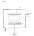
- the chamber normally includes a pair of electrodes, i.e., upper and lower electrodes, facing each other, the lower electrode being connected to an RF power source to produce a plasma between the counter electrodes.
- a silicon wafer is set immediately above the lower electrode via a mounting member, to be etched with an etchant gas in a plasma atmosphere.
- Some of the conventional plasma etching electrodes, including an upper electrode, for dry etching devices have complicated shapes to be set in a chamber structure.
- the plasma etching electrode is often composed of the components of glassy carbon, silicon or silicon carbide (SiC), and assembling these components into a monolithic structure greatly increases the cost.
- the upper electrode for a dry etching device is composed of an electrode plate of silicon or the like which is joined to a pedestal (or support ring) of metal or metal oxide by brazing with a metal, e.g., indium or silver.
- a metal e.g., indium or silver.
- joining by brazing with a metal involves problems as wafer treating temperature increases to improve the plasma etching device performance.
- the brazing metal although having a high adhesive strength, may be insufficient in resistance to heat.
- the faces joined by indium may be separated from each other, when exposed to a temperature exceeding 156°C as the melting point of indium.
- the joining needs pretreatment, e.g., undercoating treatment with a metallic film by sputtering, and other time-consuming works at high temperature, which tends to increase costs for workability and treatment.
- the brazing metal itself may cause contamination of the silicon wafer. Therefore, the joining method rarely gives good etching characteristics for dry etching, and tends to lower yield of the semiconductor device, or silicon wafer.
- USP5,074,456 proposes an upper electrode joined using a metal-filled epoxies
- USP6,073,577 proposes an upper electrode joined using a metal particles-containing elastomeric materials.
- these inventions have a lower thermal conductivity between the electrode plate and pedestal, in spite of the metallic filler present in the adhesive layer, than the case where they are joined by a brazing material, possibly causing a temperature distribution between the electrode plate periphery and center, and hence deteriorating the etching characteristics. Therefore, the joined type plasma etching electrode is required to have electrical and thermal conductance and heat resistance at the joint, and this type of plasma etching electrode excellent in these characteristics has been strongly demanded.
- the inventors of the present invention have found, after having extensively studied to develop the optimum plasma etching electrode for dry etching devices in order to solve the above problems, that the electrode plate and pedestal can be fast joined even at high temperature and, at the same time, good thermal and electrical conductance can be realized between the electrode and pedestal when graphite, which is prevented from being contaminated with an impurity, is used as the material for the pedestal and joined to the electrode plate of silicon by a polycarbodiimide-containing epoxy resin-based adhesive agent incorporated with carbon as the thermal and electrical conductive filler, reaching the present invention.
- the first invention provides a highly heat-resistant plasma etching electrode for dry etching devices, comprising an electrode plate of silicon supported by and fast, uniformly joined to a pedestal by an adhesive agent, wherein
- the second invention provides a plasma etching electrode for dry etching devices which is the same as that of the first invention wherein the adhesive agent contains 5 to 20 parts by weight of a polycarbodiimide resin and 12 to 440 parts by weight of carbon powder per 100 parts by weight of an epoxy resin.
- the third invention provides a plasma etching electrode for dry etching devices which is the same as that of the first invention wherein the adhesive agent contains a curing agent or curing promoter.
- the fourth invention provides a plasma etching electrode for dry etching devices which is the same as that of the third invention wherein the curing agent is of a compound selected from the group consisting of an amine-, hydrazine-, phenol- and acid anhydride-based compound, and the curing promoter is of a compound selected from the group consisting of imidazole, a tertiary amine and metallic complex.
- the curing agent is of a compound selected from the group consisting of an amine-, hydrazine-, phenol- and acid anhydride-based compound
- the curing promoter is of a compound selected from the group consisting of imidazole, a tertiary amine and metallic complex.
- the fifth invention provides a plasma etching electrode for dry etching devices which is the same as that of the third invention wherein the curing agent or curing promoter is incorporated at 1 to 150 parts by weight per 100 parts by weight of the epoxy resin.
- the sixth invention provides a plasma etching electrode for dry etching devices which is the same as that of the first invention wherein the polycarbodiimide resin is an aromatic-based compound.
- the seventh invention provides a plasma etching electrode for dry etching devices which is the same as that of the first invention wherein the epoxy resin is a bisphenol A type one.
- the eighth invention provides a plasma etching electrode for dry etching devices which is the same as that of the first invention wherein the carbon powder has a Young's modulus of elasticity of 6 ⁇ 10 9 to 68 ⁇ 10 9 N/m 2 .
- the ninth invention provides a plasma etching electrode for dry etching devices which is the same as that of the first invention wherein the pedestal is coated with glass-like carbon entirely except for the joint with the electrode plate of silicon.
- the tenth invention provides a plasma etching electrode for dry etching devices which is the same as that of the ninth invention wherein the coating film of glass-like carbon has a thickness of 1 to 3 ⁇ m.
- the 11 th invention provides a plasma etching electrode for dry etching devices which is the same as that of the first invention wherein the electrode plate of silicon is made of single-crystalline silicon and has through-holes.
- the 12 th invention provides a dry etching device which includes the plasma etching electrode of one of the first to 11 th inventions.
- the present invention relates to a highly heat-resistant plasma etching electrode for dry etching devices, comprising an electrode plate of silicon supported by and fast, uniformly joined to a pedestal by an adhesive agent, wherein (a) the pedestal is made of graphite, and (b) an epoxy resin containing polycarbodiimide resin and carbon powder are used for the adhesive agent.
- the preferred embodiments of the invention include the following:
- the plasma etching electrode of the present invention is highly resistant to heat, comprising an electrode plate of silicon supported by and fast, uniformly joined to a pedestal by an adhesive agent, wherein
- a plasma etching electrode i.e., upper electrode
- a plasma etching electrode is normally divided into at least 2 members, one actually facing the wafer and responsible for distributing the gases, and the other being fixed to the device.
- the member facing the wafer and responsible for distributing the gases is the electrode plate, often of silicon.
- the member fixed to the device i.e., pedestal
- the electrode plate, pedestal and joint are described.
- An electrode plate of silicon is a normal choice for the plasma etching electrode of the present invention. It is in the form of disk having a number of holes on the plate surface, through which the etchant gas is ejected. The etchant gas is converted into plasma while passing through the holes in the upper electrode, and the silicon wafer set on the lower electrode is etched with the reactive ions it attracts from the plasma.
- Silicon serving as the base for the electrode plate is not limited, but preferably single-crystalline, highly pure and dense silicon is used.
- One of the examples of such silicon is P-type single-crystal silicon doped with boron (B), having the crystal orientation of ⁇ 100>. Its resistivity is normally in a range from 1 ⁇ •cm to 30 ⁇ •cm.
- the plasma etching electrode of the present invention includes a pedestal (or support ring) normally of graphite which comes into contact with the back side of the electrode plate of silicon.
- the pedestal of graphite brings the effect of cooling the heat generated at the upper electrode (the thermal conducting effect), while being kept away from the contamination during the etching process with an impurity in the silicon wafer.
- the pedestal of graphite also serving as the cooling ring, is preferably, or should be highly heat conducting (having a high heat conductivity) and small in difference in thermal expansion coefficient with the electrode plate of silicon. Otherwise, there is a temperature gradient between the disk center and periphery of the electrode, which can be one of the causes for uneven etching characteristics.
- the pedestal of low heat conductivity and largely different from the electrode plate in thermal expansion coefficient may not well cope with the requirements for, e.g., increasing silicon wafer size, increasing treatment temperature, or adoption of rapidly heating/cooling cycles.
- Graphite serving as the base for the pedestal is not limited, but preferably highly pure to cause no contamination with an impurity during the silicon wafer etching process, and to have a high thermal conductivity and small difference in thermal expansion coefficient with the electrode plate of silicon.
- One of the examples of such graphite is the semiconductor-grade one, and the commercial products include CX-2123, CX-2114, CX-2206 and E+25 (LE-CARBONE), and EGF-262 and EGF-264 (Nippon Carbon).
- the pedestal of graphite may be of a composite of graphite and glass like carbon.
- the graphite surface is coated with glass like carbon, at least for the portion exposed to the etchant gas during the dry etching process, i.e., the portion other than that joined to the electrode plate of silicon.
- the portions include the side and back of the pedestal.
- the graphite surface is coated with glass like carbon normally to a thickness of 1 to 3 ⁇ m.
- the coating method is not limited, and may be adequately selected from the conventional ones.
- the preferable ones include to coat the graphite with a certain type of resin, e.g., polycarbodiimide or phenolic resin by spraying or impregnation, and fire the resin into the glass like carbon.
- the glass like carbon may be formed also from the pedestal surface to the inside, and thickness of the whole glass like carbon layer can be increased to 3 ⁇ m or more.
- the glass like carbon layer works as the protective layer for the graphite, controlling formation of dust from the graphite and making it more resistant to corrosion. In particular, it controls release of the gas from the graphite in the plasma atmosphere during the dry etching process, and prevents contamination of the wafer with, e.g., particles of the substances that constitute the oxide layer, separated from the graphite surface and deposited on the wafer.
- Glass like carbon is also referred to as non-graphitizable carbon or hard carbon. It is not limited with respect to the stock or production method, so long as it is produced by solid-phase carbonization of an organic substance.
- the stocks for glass like carbon include cellulose, thermosetting resins, e.g., furfuryl alcohol, and thermoplastic resins. Various methods have been proposed to produce glass like carbon from these stock materials.
- the above-described two or more members are joined to each other by the aid of a specific epoxy-based adhesive agent, described later.
- the joint layer should be electroconductive, because the assembly is set in the device in which a plasma is generated.
- the joint should be also thermally conductive, to improve the heat exchanging efficiency at the portion fixed to the device, which is cooled to cool the wafer face directly exposed to the plasma.
- the joint should be also sufficiently resistant to heat, because it may be exposed to a temperature up to 200°C on the gas distributed side.
- the adhesive agent for joining the members for the present invention contains an epoxy resin and carbon powder, the former containing a polycarbodiimide resin.
- a silicone-based adhesive agent may be considered as the heat-resistant one, to join the members at a low cost.
- its thermal expansion coefficient is 10 -4 /°C, which differs from that of silicon and graphite (10 -6 /°C) as the materials for the members to be joined by 2 digits at a high temperature atmosphere, with the result that they may be separated from each other. Therefore, it is not a choice for the present invention.
- An epoxy-based adhesive agent has a thermal expansion coefficient of the order of 10 -5 /°C, reducing possibility of the member separation, because of smaller difference in thermal expansion coefficient.
- the polycarbodiimide resin useful for the present invention may be produced by various methods. Basically, the polycarbodiimide with isocyanate at the terminal, produced by the conventional method of producing polycarbodiimide resin (refer to USP 2,941,956 and Japanese Patent Publication No.47-33279), can be used. More specifically, it is produced by the condensation involving removal of carbon dioxide (i.e., decarboxylation condensation) of an organic polyisocyanate.
- the organic polyisocyanates as the stocks for synthesizing the polycarbodiimide include aromatic polyisocyanate, aliphatic polyisocyanate, alicyclic polyisocyanate and a mixture thereof. More specifically, they include 1,5-naphthalene diisocyanate, 4,4'-diphenylmethane diisocyanate, 4,4'-diphenyldimethylmethane diisocyanate, 1,3-phenylene diisocyanate, 1,4-phenylene diisocyanate, 2,4-tolylene diisocyanate, 2,6-tolylene diisocyanate, a mixture of 2,4-tolylene diisocyanate and 2,6-tolylene diisocyanate, hexamethylene diisocyanate, cyclohexane-1,4-diisocyanate, xylylene diisocyanate, isophorone diisocyanate, dicyclohexylmethane-4,4'-diis
- the one produced from at least one type of aromatic polyisocyanate is preferable for the present invention, wherein the aromatic polyisocyanate is the isocyanate having at least 2 isocyanate groups directly bonded in the aromatic ring in the molecule.
- the carbodiimide resins useful for the present invention include the aromatic-, aliphatic- and alicyclic-based compounds, of which the aromatic-based ones are particularly preferable for their resistance to heat.
- the organic diisocyanates useful for the present invention also include the ones whose polymerization degree is adequately controlled using a compound, e.g., monoisocyanate, which is reactive with the terminal isocyanate group of the carbodiimide compound.
- the monoisocyanates which can seal the terminal of polycarbodiimide to control its polymerization degree include phenyl isocyanate, tolyl isocyanate, dimethylphenyl isocyanate, cyclohexyl isocyanate, butyl isocyanate and naphthyl isocyanate.
- -OH group e.g., methanol, ethanol, phenol, cyclohexano
- the decarboxylation/condensation reaction of the organic diisocyanate proceeds in the presence of catalyst for producing carbodiimide.
- catalysts include phospholene oxides, e.g., 1-phenyl-2-phospholene-1-oxide, 3-methyl-1-phenyl-2-phospholene-1-oxide, 1-ethyl-2-phospholene-1-oxide, 3-methyl-2-phospholene-1-oxide, and a 3-phospholene isomer thereof. Of these, 3-methyl-1-phenyl-2-phospholene-1-oxide is more preferable for its reactivity.
- the polycarbodiimide resin for the present invention preferably has a number-average molecular weight of 3,000 to 50,000 as polystyrene, determined by gel permeation chromatography (GPC), more preferably 10,000 to 30,000, still more preferably 15,000 to 25,000, whether it is incorporated with the terminal sealant or not. It is sufficiently resistant to heat, when it has a number-average molecular weight of 3,000 or more. The one having a molecular weight above 50,000 is not practical, because it needs a long reaction time for synthesis.
- GPC gel permeation chromatography
- the epoxy resin for the adhesive agent for the present invention may be selected from those generally known for epoxy resin-based adhesive agents. These epoxy resins include those having 2 or more epoxy groups in the molecule, such as glycidyl ether type epoxy resins, e.g., bisphenol A, bisphenol F, phenol novolac and cresol novolac type epoxy resin; and alicyclic, glycidyl ester type, glycidyl amine type, heterocyclic and liquid-rubber-modified type epoxy resin. They may be used either individually or in combination. Of these, bisphenol A, bisphenol F, phenol novolac and cresol novolac type epoxy resin are more preferable, and bisphenol A type is still more preferable.
- the epoxy resin useful for the present invention is not limited to the above, but is preferably hardened acceleratingly in the presence of the above-described polycarbodiimide resin.
- Carbon powder for the adhesive agent for the present invention works as the thermally or electrically conductive filler which provides or improves thermal or electrical conductance of the adhesive agent, when incorporated therein by kneading.
- the known electroconductive fillers include those of metals, e.g., silver and copper, carbon powder, and fine, silver-plated powder.
- carbon (or graphite) powder is used for its thermal stability and ability of adjusting modulus of elasticity.
- the effect of carbon powder on adhesive agent conductance varies depending on its shape, particle size and content in the agent. It has a particle size of 1 to 100 ⁇ m, preferably 10 to 50 ⁇ m, and preferably has a relatively narrow particle size distribution. Moreover, it preferably has a Young's modulus of elasticity of 6 ⁇ 10 9 to 68 ⁇ 10 9 N/m 2 .
- the adhesive agent for the present invention can be prepared by mixing an epoxy resin containing at least a polycarbodiimide resin with carbon powder.
- the adhesive agent composition for the present invention normally contains a polycarbodiimide resin preferably at 5 to 20 parts by weight per 100parts by weight of the epoxy resin, viewed from the adhesive force of the agent. At below 5 parts by weight, the agent may not join the members sufficiently fast. At above 20 parts by weight, on the other hand, its effect may not be fully exhibited.
- the adhesive agent free of polycarbodiimide resin generally has a shear strength of around 15MPa (around 150kg/cm 2 ), determined by the shear strength test (JIS K6850), after it is cured.
- the shear strength gradually increases as polycarbodiimide resin content increases, attaining a maximum of 20MPa or more at the content of around 5 to 20 parts by weight.
- the carbon powder is incorporated at 10 to 90 parts by weight per 100 parts by weight of the whole adhesive agent composition, i.e., 10 to 90% by weight, preferably 30 to 80 parts by weight (i.e., 30 to 80% by weight) viewed specifically from electrical resistance of the electrode itself.
- the method of mixing is not limited; for example, the components are mixed by melt kneading using a kneader or hot roll mixer, or in the presence of an adequate solvent inert to the polycarbodiimide and epoxy resin.
- the adhesive agent for the present invention may be incorporated with one or more additives or fillers selected from those conventionally used for adhesive compositions within limits not harmful for the effect of the present invention.
- the preferable additives and fillers for the present invention include fibrous reinforcing agents, powdery or crystalline fillers (e.g., molten silica), pigments, and curing agents and curing promoters which accelerate curing by the reactions between the polycarbodiimide and epoxy resin.
- the curing agent or promoter when used, is incorporated at 1 to 150 parts by weight per 100 parts by weight of the epoxy resin, and its content can be adjusted depending on type of the epoxy resin and curing conditions.
- the curing agents useful for the present invention include amine-based compounds, e.g., dicyandiamide, hydrazine-based compounds, phenolic compounds and acid anhydrides.
- the curing promoters include imidazole, tertiary amine and metal complex, which itself bound to the adhesive agent while promoting the reactions between the epoxy resin and curing agent. These additives may be added during or after the above-described mixing step, or incorporated beforehand in one of the resins before the mixing step.
- the adhesive agent for the present invention can be transformed into the final, cured product, when heated normally at 80 to 200°C, preferably 120 to 200°C. It is considered that the adhesive agent is cured by crosslinking caused by the reactions between the carbodiimide group in the polycarbodiimide resin and epoxy group.
- the plasma etching electrode, i.e., upper electrode, of the present invention is one component of a dry etching device for production of silicon wafers.
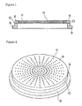
- the etching device is outlined in Figure 3, and the upper electrode in Figures 1 and 2.
- the electrode plate 8 of silicon was of P-type (doped with B) single-crystal silicon (Si) having crystal orientation of ⁇ 100> and an electrical resistivity of 15 ⁇ cm, formed into the shape having dimensions of 223.5mm in diameter and 6.35mm in thickness, and provided with 3200 etchant gas ejecting holes (diameter: 0.8mm).
- the graphite ring (pedestal) 9 was of graphite (LE-CARBONE's E+25), formed into the shape having dimensions of 223.5mm in diameter and 19mm in thickness, and provided with a collar by which the ring was fixed to the device.
- the electrode plate 8 of silicon was joined to the graphite ring 9 via the joint 10, to form the plasma etching electrodes 1 to 6, where the joint 10 was comprised an adhesive agent prepared by kneading 10 parts by weight of an aromatic-based polycarbodiimide resin (Nisshinbo Industries' Carbodilite 10M-SPTM), 10 parts by weight of dicyandiamide as the curing agent and 2 parts by weight of imidazole as the curing promoter per 100 parts by weight of a bisphenol A type epoxy resin, and also 12, 47, 73, 110, 257 or 440 parts by weight of graphite powder (Kawasaki Steel's HA2500F) per 100 parts by weight of the epoxy resin.
- an adhesive agent prepared by kneading 10 parts by weight of an aromatic-based polycarbodiimide resin (Nisshinbo Industries' Carbodilite 10M-SPTM), 10 parts by weight of dicyandiamide as the curing agent and 2 parts by weight of imidazo
- the plasma etching electrode thus prepared was used as the component for a dry etching device for production of silicon wafers.
- the plasma etching electrode was set in the dry etching device (LAM RESEARCH's Exel 4250) was evaluated for overall electrical resistance, etching rate and resistance of the joint to heat (measured by presence or absence of the separation after it was exposed to 6,000 cycles of wafer etching at 2,000W for 5 minutes and cooling for 2 minutes).
- the overall electrical resistance was determined by an analyzer (Mitsubishi Chemical's MCP-T600). The evaluation results are given in Table 1.
- Electrodes Graphite powder content (parts by weight per 100 parts by weight of the epoxy resin) Overall electrical resistance ( ⁇ ) Etching rate ( ⁇ ) Resistance to heat EXAMPLE 1 12 2.2 ⁇ 10 6 5980 No separation observed EXAMPLE 2 47 4.8 ⁇ 10 5 6050 No separation observed EXAMPLE 3 73 9.2 ⁇ 10 4 6220 No separation observed EXAMPLE 4 110 2.3 ⁇ 10 3 6290 No separation observed EXAMPLE 5 257 9.3 ⁇ 10 2 6310 No separation observed EXAMPLE 6 440 1.2 ⁇ 10 2 6320 No separation observed
- the joint 10 of the electrode prepared in each of EXAMPLES 1 to 6 was sufficiently resistant to heat not to be separated during the testing period.
- the joint 10 of the electrode prepared in each of COMPARATIVE EXAMPLES 1 to 3 was less resistant to heat and separated during the testing period. Therefore, the plasma etching electrode of the present invention is excellent to improve the chip production yield. It is accepted that the preferable etching rate standard is in a range of 6300 ⁇ 300 ⁇ , and the electrodes prepared in EXAMPLES 2 to 6 meet the standard.
- the carbodiimide-containing epoxy-based adhesive agent containing the graphite powder at above 440 parts by weight was difficult to spread on the joint 10 due to increased viscosity, and it is considered that it would show an etching rate almost the same as that observed in EXAMPLE 6. It is therefore found that the optimum graphite content is in a range of 47 to 440 parts by weight per 100 parts by weight of the epoxy resin with respect to etching rate.
- the plasma etching electrode of the present invention is highly resistant to heat, comprising an electrode plate of silicon supported by and fast, uniformly joined to a pedestal by an adhesive agent, wherein (a) the pedestal is made of graphite, and (b) an epoxy resin containing polycarbodiimide resin and carbon powder are used for the adhesive agent.
- This structure allows the electrode to work at a high temperature at which the electrode prepared with the aid of the conventional adhesive agent is unserviceable, and improves electrical and thermal conductance of the electrode. It also brings the favorable effect of realizing good etching characteristics without causing contamination with an impurity, thereby improving semiconductor device production yield.
- the electrode plate can be joined to the pedestal at room temperature without needing the undercoating treatment or the like, and hence at a lower cost.
Landscapes
- Chemical & Material Sciences (AREA)
- Physics & Mathematics (AREA)
- Engineering & Computer Science (AREA)
- Plasma & Fusion (AREA)
- Analytical Chemistry (AREA)
- Organic Chemistry (AREA)
- Drying Of Semiconductors (AREA)
- Adhesives Or Adhesive Processes (AREA)
- Plasma Technology (AREA)
Applications Claiming Priority (4)
| Application Number | Priority Date | Filing Date | Title |
|---|---|---|---|
| JP2002118861 | 2002-04-22 | ||
| JP2002118861 | 2002-04-22 | ||
| JP2002187529 | 2002-06-27 | ||
| JP2002187529A JP3868341B2 (ja) | 2002-04-22 | 2002-06-27 | 耐熱性に優れたプラズマエッチング電極及びそれを装着したドライエッチング装置 |
Publications (2)
| Publication Number | Publication Date |
|---|---|
| EP1357576A2 true EP1357576A2 (fr) | 2003-10-29 |
| EP1357576A3 EP1357576A3 (fr) | 2006-04-26 |
Family
ID=28793605
Family Applications (1)
| Application Number | Title | Priority Date | Filing Date |
|---|---|---|---|
| EP02356151A Withdrawn EP1357576A3 (fr) | 2002-04-22 | 2002-07-31 | Electrode résistante à la chaleur pour décapage à plasma, et dispositif pour décapage à plasma comportant celle-ci |
Country Status (7)
| Country | Link |
|---|---|
| US (1) | US6818097B2 (fr) |
| EP (1) | EP1357576A3 (fr) |
| JP (1) | JP3868341B2 (fr) |
| KR (1) | KR20030084540A (fr) |
| CN (1) | CN1453830A (fr) |
| SG (1) | SG109978A1 (fr) |
| TW (1) | TW552638B (fr) |
Cited By (3)
| Publication number | Priority date | Publication date | Assignee | Title |
|---|---|---|---|---|
| WO2011090668A3 (fr) * | 2009-12-29 | 2011-11-24 | 3M Innovative Properties Company | Compositions époxydiques, et films de surfaçage obtenus à partir de ces compositions |
| KR20170066206A (ko) * | 2015-11-16 | 2017-06-14 | 어플라이드 머티어리얼스, 인코포레이티드 | 저 증기압 에어로졸-보조 cvd |
| KR20210028632A (ko) * | 2015-11-16 | 2021-03-12 | 어플라이드 머티어리얼스, 인코포레이티드 | 저 증기압 에어로졸-보조 cvd |
Families Citing this family (44)
| Publication number | Priority date | Publication date | Assignee | Title |
|---|---|---|---|---|
| US8048806B2 (en) | 2000-03-17 | 2011-11-01 | Applied Materials, Inc. | Methods to avoid unstable plasma states during a process transition |
| US7220937B2 (en) * | 2000-03-17 | 2007-05-22 | Applied Materials, Inc. | Plasma reactor with overhead RF source power electrode with low loss, low arcing tendency and low contamination |
| KR101075046B1 (ko) * | 2002-05-23 | 2011-10-19 | 램 리써치 코포레이션 | 반도체 공정용 플라즈마 반응기를 위한 다중부재 전극 및다중부재 전극의 일부를 교체하는 방법 |
| US7901952B2 (en) | 2003-05-16 | 2011-03-08 | Applied Materials, Inc. | Plasma reactor control by translating desired values of M plasma parameters to values of N chamber parameters |
| US7247218B2 (en) | 2003-05-16 | 2007-07-24 | Applied Materials, Inc. | Plasma density, energy and etch rate measurements at bias power input and real time feedback control of plasma source and bias power |
| US7470626B2 (en) | 2003-05-16 | 2008-12-30 | Applied Materials, Inc. | Method of characterizing a chamber based upon concurrent behavior of selected plasma parameters as a function of source power, bias power and chamber pressure |
| US7910013B2 (en) | 2003-05-16 | 2011-03-22 | Applied Materials, Inc. | Method of controlling a chamber based upon predetermined concurrent behavior of selected plasma parameters as a function of source power, bias power and chamber pressure |
| US7795153B2 (en) | 2003-05-16 | 2010-09-14 | Applied Materials, Inc. | Method of controlling a chamber based upon predetermined concurrent behavior of selected plasma parameters as a function of selected chamber parameters |
| US7452824B2 (en) | 2003-05-16 | 2008-11-18 | Applied Materials, Inc. | Method of characterizing a chamber based upon concurrent behavior of selected plasma parameters as a function of plural chamber parameters |
| JP4118194B2 (ja) * | 2003-06-02 | 2008-07-16 | 横河電機株式会社 | 洗浄装置 |
| US20060169209A1 (en) * | 2005-02-01 | 2006-08-03 | Tokyo Electon Limited | Substrate processing apparatus, substrate processing method, and storage medium storing program for implementing the method |
| KR100708321B1 (ko) | 2005-04-29 | 2007-04-17 | 주식회사 티씨케이 | 플라즈마 식각장치의 캐소드 전극 결합구조 |
| US8789493B2 (en) | 2006-02-13 | 2014-07-29 | Lam Research Corporation | Sealed elastomer bonded Si electrodes and the like for reduced particle contamination in dielectric etch |
| JP4935149B2 (ja) * | 2006-03-30 | 2012-05-23 | 東京エレクトロン株式会社 | プラズマ処理用の電極板及びプラズマ処理装置 |
| US8216418B2 (en) * | 2007-06-13 | 2012-07-10 | Lam Research Corporation | Electrode assembly and plasma processing chamber utilizing thermally conductive gasket and o-rings |
| KR100813106B1 (ko) * | 2007-09-19 | 2008-03-17 | 다이섹(주) | 가압접합된 캐소드 및 그 제조방법 |
| US8187414B2 (en) * | 2007-10-12 | 2012-05-29 | Lam Research Corporation | Anchoring inserts, electrode assemblies, and plasma processing chambers |
| US8152954B2 (en) * | 2007-10-12 | 2012-04-10 | Lam Research Corporation | Showerhead electrode assemblies and plasma processing chambers incorporating the same |
| US8187413B2 (en) * | 2008-03-18 | 2012-05-29 | Lam Research Corporation | Electrode assembly and plasma processing chamber utilizing thermally conductive gasket |
| KR100977315B1 (ko) | 2008-04-10 | 2010-08-23 | 티씨비코리아(주) | 플라즈마 챔버용 캐소드 전극 및 그 제조방법 |
| US8679288B2 (en) | 2008-06-09 | 2014-03-25 | Lam Research Corporation | Showerhead electrode assemblies for plasma processing apparatuses |
| TWD136587S1 (zh) * | 2008-07-22 | 2010-08-21 | 東京威力科創股份有限公司 | 晶圓吸附板 |
| US8449679B2 (en) | 2008-08-15 | 2013-05-28 | Lam Research Corporation | Temperature controlled hot edge ring assembly |
| US8147648B2 (en) * | 2008-08-15 | 2012-04-03 | Lam Research Corporation | Composite showerhead electrode assembly for a plasma processing apparatus |
| TWI511619B (zh) * | 2009-07-03 | 2015-12-01 | Advanced Micro Fab Equip Inc | Electrode elements for plasma processing, internal components and methods for their manufacture and separation |
| JP5713182B2 (ja) * | 2011-01-31 | 2015-05-07 | 三菱マテリアル株式会社 | プラズマエッチング用シリコン電極板 |
| USD664249S1 (en) * | 2011-07-01 | 2012-07-24 | Applied Materials, Inc. | Flow blocker plate |
| USD709539S1 (en) | 2011-09-30 | 2014-07-22 | Tokyo Electron Limited | Focusing ring |
| USD699199S1 (en) * | 2011-09-30 | 2014-02-11 | Tokyo Electron Limited | Electrode plate for a plasma processing apparatus |
| USD709538S1 (en) | 2011-09-30 | 2014-07-22 | Tokyo Electron Limited | Focusing ring |
| USD699200S1 (en) * | 2011-09-30 | 2014-02-11 | Tokyo Electron Limited | Electrode member for a plasma processing apparatus |
| USD709536S1 (en) | 2011-09-30 | 2014-07-22 | Tokyo Electron Limited | Focusing ring |
| USD709537S1 (en) | 2011-09-30 | 2014-07-22 | Tokyo Electron Limited | Focusing ring |
| JP2014035888A (ja) * | 2012-08-09 | 2014-02-24 | Toyota Motor Corp | 全固体電池及びその製造方法 |
| US9314854B2 (en) | 2013-01-30 | 2016-04-19 | Lam Research Corporation | Ductile mode drilling methods for brittle components of plasma processing apparatuses |
| US8893702B2 (en) | 2013-02-20 | 2014-11-25 | Lam Research Corporation | Ductile mode machining methods for hard and brittle components of plasma processing apparatuses |
| CN104974469B (zh) * | 2015-07-07 | 2017-11-28 | 苏州生益科技有限公司 | 一种树脂组合物及使用其制作的半固化片及层压板 |
| JP6146841B1 (ja) * | 2016-08-04 | 2017-06-14 | 日本新工芯技株式会社 | リング状電極 |
| CN108329032B (zh) * | 2017-12-21 | 2021-02-23 | 山东道普安制动材料有限公司 | 一种汽车碳陶刹车盘的修复方法 |
| CN108336181B (zh) * | 2018-01-24 | 2019-11-01 | 南通鸿图健康科技有限公司 | 一种太阳能电池及其制备方法 |
| CN113939894B (zh) * | 2019-06-08 | 2024-07-23 | 应用材料公司 | 具有耐化学性表面的rf组件 |
| CN120854248A (zh) * | 2019-06-12 | 2025-10-28 | 朗姆研究公司 | 用于等离子体处理室部件的密封剂涂层 |
| CN111048395A (zh) * | 2019-12-26 | 2020-04-21 | 苏州珮凯科技有限公司 | 8寸晶圆制造蚀刻机台Unity-85核心零部件上部电极表面制程物的去除方法 |
| USD1092423S1 (en) * | 2022-05-19 | 2025-09-09 | Asm Ip Holding B.V. | Electrode plate for semiconductor manufacturing apparatus |
Family Cites Families (16)
| Publication number | Priority date | Publication date | Assignee | Title |
|---|---|---|---|---|
| DE3609687A1 (de) * | 1985-03-29 | 1986-10-02 | Nisshinbo Industries, Inc., Tokio/Tokyo | Duroplastisches harz und verfahren zu seiner erzeugung |
| US5223584A (en) * | 1989-07-11 | 1993-06-29 | Gencorp Inc. | In situ thermoset molecular composites |
| US5074456A (en) * | 1990-09-18 | 1991-12-24 | Lam Research Corporation | Composite electrode for plasma processes |
| EP0573915A1 (fr) * | 1992-06-12 | 1993-12-15 | Nisshinbo Industries, Inc. | Plaque d'électrode et gabarit pour utilisation un gravure par plasma |
| JPH0616907A (ja) * | 1992-06-29 | 1994-01-25 | Nisshinbo Ind Inc | 導電性組成物及び該導電性組成物による接着剤又は塗料 |
| JPH0758086A (ja) * | 1993-08-11 | 1995-03-03 | Ibiden Co Ltd | プラズマエッチング用電極板 |
| JPH0799183A (ja) * | 1993-09-28 | 1995-04-11 | Nisshinbo Ind Inc | プラズマエッチング電極、その治具及びそれらの製造方法 |
| US5576398A (en) * | 1995-07-07 | 1996-11-19 | Japan Synthetic Rubber Co., Ltd. | Thermosetting resin composition |
| JPH09241353A (ja) * | 1996-03-13 | 1997-09-16 | Japan Synthetic Rubber Co Ltd | エポキシ樹脂用硬化剤 |
| JP3454333B2 (ja) * | 1996-04-22 | 2003-10-06 | 日清紡績株式会社 | プラズマエッチング電極 |
| US6083644A (en) * | 1996-11-29 | 2000-07-04 | Seiko Instruments Inc. | Non-aqueous electrolyte secondary battery |
| JP3467400B2 (ja) * | 1998-01-13 | 2003-11-17 | 日清紡績株式会社 | 液状封止材用樹脂組成物及び液状封止材 |
| EP0943642A1 (fr) * | 1998-03-20 | 1999-09-22 | Nisshinbo Industries, Inc. | Copolymère de polycarbodiimide et procédé de fabrication |
| US6073577A (en) * | 1998-06-30 | 2000-06-13 | Lam Research Corporation | Electrode for plasma processes and method for manufacture and use thereof |
| JP3482153B2 (ja) * | 1999-04-09 | 2003-12-22 | 住友ベークライト株式会社 | 半導体用ダイアタッチペースト |
| JP2002093777A (ja) * | 2000-07-11 | 2002-03-29 | Nisshinbo Ind Inc | ドライエッチング装置 |
-
2002
- 2002-06-27 JP JP2002187529A patent/JP3868341B2/ja not_active Expired - Fee Related
- 2002-07-06 KR KR1020020039104A patent/KR20030084540A/ko not_active Withdrawn
- 2002-07-10 SG SG200204184A patent/SG109978A1/en unknown
- 2002-07-22 US US10/199,465 patent/US6818097B2/en not_active Expired - Fee Related
- 2002-07-30 CN CN02126995A patent/CN1453830A/zh active Pending
- 2002-07-30 TW TW091116984A patent/TW552638B/zh not_active IP Right Cessation
- 2002-07-31 EP EP02356151A patent/EP1357576A3/fr not_active Withdrawn
Non-Patent Citations (1)
| Title |
|---|
| None * |
Cited By (3)
| Publication number | Priority date | Publication date | Assignee | Title |
|---|---|---|---|---|
| WO2011090668A3 (fr) * | 2009-12-29 | 2011-11-24 | 3M Innovative Properties Company | Compositions époxydiques, et films de surfaçage obtenus à partir de ces compositions |
| KR20170066206A (ko) * | 2015-11-16 | 2017-06-14 | 어플라이드 머티어리얼스, 인코포레이티드 | 저 증기압 에어로졸-보조 cvd |
| KR20210028632A (ko) * | 2015-11-16 | 2021-03-12 | 어플라이드 머티어리얼스, 인코포레이티드 | 저 증기압 에어로졸-보조 cvd |
Also Published As
| Publication number | Publication date |
|---|---|
| SG109978A1 (en) | 2005-04-28 |
| JP2004006561A (ja) | 2004-01-08 |
| EP1357576A3 (fr) | 2006-04-26 |
| US20030196759A1 (en) | 2003-10-23 |
| US6818097B2 (en) | 2004-11-16 |
| CN1453830A (zh) | 2003-11-05 |
| TW552638B (en) | 2003-09-11 |
| KR20030084540A (ko) | 2003-11-01 |
| JP3868341B2 (ja) | 2007-01-17 |
Similar Documents
| Publication | Publication Date | Title |
|---|---|---|
| US6818097B2 (en) | Highly heat-resistant plasma etching electrode and dry etching device including the same | |
| EP1195083B1 (fr) | Materiau de sous-remplissage pour substrats de semi-conducteurs | |
| JPH0329207A (ja) | 回路接続用組成物及びこれを用いた接続方法並びに半導体チップの接続構造 | |
| CN102066488A (zh) | 热互连和界面材料、它们的制造方法和用途 | |
| US6491784B2 (en) | Dry etching device | |
| EP0928825A2 (fr) | Composition de résine pour l'utilisation dans des matériaux de scellement et matériau de scellement liquide utilisant la composition de résine | |
| JP4507488B2 (ja) | 接合材料 | |
| CN1105161C (zh) | 导热软膏 | |
| KR20060126903A (ko) | 접착제 및 그 제조 방법 | |
| JP3991268B2 (ja) | 回路部材接続用フィルム状接着剤及びこれを用いた半導体装置 | |
| CN1185231A (zh) | 半导体单元的封装体、其封装方法及其封装材料 | |
| WO2010131655A1 (fr) | Feuillet de liaison | |
| JPH11349905A (ja) | 熱伝導性感圧接着シ―ト類 | |
| EP0990686B1 (fr) | Film adhésif pour boitier de semi-conducteur | |
| JP2026061821A (ja) | シート状硬化物、複合成形体及びパワー半導体装置 | |
| KR102507422B1 (ko) | 반도체 소자 밀봉용 에폭시 수지 조성물 및 이를 사용하여 밀봉된 반도체 소자 | |
| KR20250112693A (ko) | 기대, 정전 척 장치 및 기대의 제조 방법 | |
| US4488283A (en) | Epoxy resin | |
| JP5283234B2 (ja) | 導電性樹脂組成物及びそれを用いた半導体装置 | |
| KR20250085297A (ko) | 반도체 소자 밀봉용 에폭시 수지 조성물 및 이를 사용하여 밀봉된 반도체 소자 | |
| JPH06181227A (ja) | 接着剤及び半導体装置 | |
| JP2025084570A (ja) | 熱伝導性樹脂組成物、及び半導体装置 | |
| JPH1060398A (ja) | 接着剤、半導体装置の製造方法、および半導体装置 | |
| JP2026021971A (ja) | 硬化物、複合成形体、半導体デバイス及び複合成形体の製造方法 | |
| JP2003234019A (ja) | 絶縁性ペースト |
Legal Events
| Date | Code | Title | Description |
|---|---|---|---|
| PUAI | Public reference made under article 153(3) epc to a published international application that has entered the european phase |
Free format text: ORIGINAL CODE: 0009012 |
|
| AK | Designated contracting states |
Kind code of ref document: A2 Designated state(s): AT BE BG CH CY CZ DE DK EE ES FI FR GB GR IE IT LI LU MC NL PT SE SK TR |
|
| AX | Request for extension of the european patent |
Extension state: AL LT LV MK RO SI |
|
| PUAL | Search report despatched |
Free format text: ORIGINAL CODE: 0009013 |
|
| AK | Designated contracting states |
Kind code of ref document: A3 Designated state(s): AT BE BG CH CY CZ DE DK EE ES FI FR GB GR IE IT LI LU MC NL PT SE SK TR |
|
| AX | Request for extension of the european patent |
Extension state: AL LT LV MK RO SI |
|
| RIN1 | Information on inventor provided before grant (corrected) |
Inventor name: TOMITA, HIDESHI Inventor name: YAMAGUCHI, AKIRA |
|
| 17P | Request for examination filed |
Effective date: 20060807 |
|
| AKX | Designation fees paid |
Designated state(s): DE |
|
| 17Q | First examination report despatched |
Effective date: 20070214 |
|
| STAA | Information on the status of an ep patent application or granted ep patent |
Free format text: STATUS: THE APPLICATION IS DEEMED TO BE WITHDRAWN |
|
| 18D | Application deemed to be withdrawn |
Effective date: 20100202 |