EP1357578A2 - Dispositif et méthode pour l' analyse de surface par spectroscopie - Google Patents
Dispositif et méthode pour l' analyse de surface par spectroscopie Download PDFInfo
- Publication number
- EP1357578A2 EP1357578A2 EP03252540A EP03252540A EP1357578A2 EP 1357578 A2 EP1357578 A2 EP 1357578A2 EP 03252540 A EP03252540 A EP 03252540A EP 03252540 A EP03252540 A EP 03252540A EP 1357578 A2 EP1357578 A2 EP 1357578A2
- Authority
- EP
- European Patent Office
- Prior art keywords
- electrons
- gating
- flight
- voltage
- flight tube
- Prior art date
- Legal status (The legal status is an assumption and is not a legal conclusion. Google has not performed a legal analysis and makes no representation as to the accuracy of the status listed.)
- Withdrawn
Links
Images

Classifications
-
- H—ELECTRICITY
- H01—ELECTRIC ELEMENTS
- H01J—ELECTRIC DISCHARGE TUBES OR DISCHARGE LAMPS
- H01J49/00—Particle spectrometers or separator tubes
- H01J49/26—Mass spectrometers or separator tubes
- H01J49/34—Dynamic spectrometers
- H01J49/40—Time-of-flight spectrometers
Definitions
- the present invention relates to a spectroscopic analyser for surface analysis, and to a method for surface analysis spectroscopy.
- the invention relates particularly (but not exclusively) to the determination of energy of electrons emitted from the surface of a material during X-ray photoelectron or Auger electron spectroscopy.
- the chemical composition and properties of the top few atomic layers of a material to be analysed are of interest. These parameters are determined by measuring the characteristic energy distribution of electrons emitted from the surface of a sample of the material under investigation.
- the surface is irradiated by a suitable exciting beam and emitted electrons are collected into an electron spectrometer, in which their energies are determined.
- XPS X-ray photoelectron spectroscopy
- AES Auger electron spectroscopy
- the core holes arising from this are filled again by relaxation of the atoms, in which electrons with lower binding energies drop down into the holes.
- the energy released by these de-excitation processes results in the emission of X-rays or Auger electrons.
- the energies of these Auger electrons are, again, characteristic of the elements from which they derive and can thus be used to identify the elements present in the surface of the sample.
- a wide variety of energy analysers has been used to perform such surface analysis measurements, but the preferred techniques involve the use of either a toroidal electrostatic analyser or an electrostatic cylindrical mirror analyser. These analysers provide measurements of high energy resolution, but are limited in the range of energies which can be analysed in a single measurement. This range is typically less than 50 eV, while the full energy range of the emitted electrons may be from 50 eV to 2500 eV. Therefore, in order to perform an analysis of the whole range of energies of interest, the analyser must scan through this range, by sweeping the voltages applied to the electrostatic deflection plates, under computer control. Clearly, this procedure is inefficient, since, at any time during electron detection, the majority of the electrons being emitted from the sample are outside the range of energies under analysis and are therefore not detected.
- WO 99/35668 discloses an electron energy analyser, using a hyperbolic electrostatic field to deflect the electrons onto a detector.
- US-A-5,969,354 relates to an electron analyser, in which a solenoid sets up an axial magnetic field in a drift region of the analyser. The electrons gyrate around the magnetic field lines and the amount of rotation of the electrons exiting the region depends on their energies.
- Both analysers record the position of the electrons on detector plates, in order to obtain a measurement of energy. While these analysers provide good energy resolution, they do suffer from a number of limitations, such as providing poor access to the sample, being able to accommodate only a limited sample size, and requiring complicated detection electronics.
- excited electrons are emitted from the sample in all directions. It is, therefore, also desirable to collect the electrons over as large a solid angle as possible.
- a high collection efficiency is usually accomplished using an electron lens to focus a diverging beam of electrons from the sample into the analyser. Electrostatic lenses and magnetic lenses have been used for this purpose, but both types of lens are unable to focus electrons having widely ranging energies, so are unsuitable for use in an analyser for the desired application. Without the use of an electron lens, the acceptance angle of a conventional analyser would be very small, typically less than 1°.
- Strong permanent magnets located behind the sample have been used to constrain the trajectories of the emitted electrons.
- a magnetic field gradient such as that used in "Apparatus for positron annihilation-induced Auger electron spectroscopy" by Chun et al. (Review of Scientific Instruments, vol. 60, no. 12, December 1989), reduces the angular spread of the emitted electrons and redirects them along the spectrometer axis.
- an analyser is not suitable for electron beam Auger analysis.
- a spectroscopic analyser comprising: means for irradiating a surface of a material to be analysed; and a time of flight (ToF) spectrometer including: gating means at an entrance to the TOF spectrometer, the gating means being arranged to receive and selectively pass at least a part of a beam of electrons emitted from the surface of the material to be analysed, as one or more pulses of emitted electrons; a flight tube along which the or each pulse of emitted electrons is arranged to pass; and a detector arrangement downstream of the gating means and being arranged to detect the arrival of electrons within the or each pulse from the gating means via the flight tube, and to permit determination of the times of flight of the detected electrons through the flight tube.
- ToF time of flight
- the spectroscopic analyser of the present invention provides a number of advantages over prior art analysers.
- the use of a time-of-flight energy spectrometer permits simultaneous detection of electrons having a wide range of energies (not least because the arrangement requires no input lens), and is operable over a wide solid angle. Nevertheless, high energy resolution is still possible.
- the overall detection efficiency is high which means that low doses of irradiation can be employed and the overall acquisition time at the detector can be kept short.
- the arrangement of the present invention also allows for ready access to a sample of material to be analysed without limiting its size.
- the invention is particularly suitable for X-ray photoelectron spectroscopy and Auger electron spectroscopy.
- the surface of the material to be analysed is irradiated with X-rays which cause secondary electrons to be emitted and these are gated into the time-of-flight spectrometer in pulses.
- primary electrons bombard the surface of the material to be analysed and, again, secondary electrons are emitted which are gated into the time-of-flight spectrometer.
- Time-of-flight spectrometers are well known in the field of mass spectrometry, where it is desirable to determine the mass-to-charge ratio of ions or molecules. In such time-of-flight spectrometers, however, it is usual to accelerate the particles whose mass-to-charge ratio is to be determined using an electrostatic field. In that case, the energy which the particles have within the time-of-flight mass spectrometer, 1 ⁇ 2mv 2 , is equated to the energy gained by the particles in the electrostatic field, qV, where V is electrical potential and q is the charge on the ion.
- time-of-flight is proportional to the square root of the mass-to-charge ratio.
- the time-of-flight spectrometer in the present invention does not measure mass-to-charge ratios, as it is instead the energy of the particles emitted from the surface of the sample to be analysed that is of interest.
- no acceleration potential is needed between the surface of the sample and the inlet to the flight tube of the TOF spectrometer.
- the time-of-flight of the particles emitted from the surface of the material to be analysed is proportional to E -1 ⁇ 2 for particles of a given mass.
- the mass is simply the mass of an electron in each case so the electrons separate in time-of-flight in accordance with their energies.
- a pulse of electrons gated into the time-of-flight spectrometer will accordingly spread out over the length of the flight tube with the more energetic electrons arriving before the less energetic electrons.
- the spectroscopic analyser further comprises a mirror mounted within the flight tube of the TOF spectrometer and arranged to reflect electrons within the pulse of emitted electrons so that the electrons traverse at least a part of the length of the flight tube in generally opposing directions.
- a mirror mounted within the flight tube of the TOF spectrometer and arranged to reflect electrons within the pulse of emitted electrons so that the electrons traverse at least a part of the length of the flight tube in generally opposing directions.
- Employing a mirror allows the effective path length traversed by the electrons within the flight tube to be increased for a given length of flight tube.
- the mirror is generally spherical in shape, since this permits a wide range of electron energies to be refocused to the detector.
- a toroidal or elliptical mirror may be employed as an alternative.
- the mirror of preferred embodiments of the present invention may be of magnetic or electrostatic design.
- the mirror comprises first and second transparent concentric meshes spaced along a longitudinal axis of the flight tube.
- the first mesh is maintained in use at a first, ground potential
- the second mesh is maintained in use at a second voltage which is greater than the maximum energy of interest of the electrons in the flight tube.
- the electrons may be retarded before entry into the flight tube to a much lower energy. This may be accomplished, for example, by the use of a retarding mesh or lens between the surface of the material to be analysed and the gating means.
- the gating means opens and closes to the passage of the beam of emitted electrons under the control of an applied voltage or current. Most simply, this may be achieved using a retarding voltage which is greater than the maximum electron energy. Most favourably, however, gating is achieved by the deflection of the emitted electrons from their normal flight path into a trajectory where they can no longer reach the detector. This may be achieved by a magnetic or electrostatic deflection.
- the gating means comprises a plurality of gating members disposed across the entrance to the flight tube, and defining therebetween a plurality of entrance channels for the emitted electrons.
- the spectroscopic analyser may further comprise means for generating voltages of opposing polarity, a first output thereof, of a first polarity, being connected in use to even ones of the plurality of gating members, and a second output thereof, of a second polarity, being connected in use to odd ones of the plurality of gating members.
- the beam of emitted electrons may pass through the channels defined between the gating members, which are preferably plates, without obstruction.
- the beam of emitted electrons is deflected away from the trajectory of the unobstructed beam.
- the electrons deflected by the gating members in this way may be directed towards baffles (not shown), which are specifically located downstream of the gating means to intercept the electrons.
- the deflected electrons may be intercepted by colliding with the gating members themselves, or with the walls of the flight tube. The interception of the electrons may occur either upstream or downstream of the electron mirror, depending on the voltages applied to the gating members.
- the electrons On arrival at these sites, the electrons are either absorbed, or scattered, producing low energy electrons which contribute to a background count rate in the spectrum detected at the detector. It is possible to eliminate the count rate of the very low energy electrons arriving at the detector by applying a small negative bias at the front of the detector.
- odd ones of the plurality of gating members are connected in use to a ground potential and even ones of the plurality of gating members are connected in use to the first or second output of the means for generating voltages. This allows for simplification of the electronics.
- pulses may be generated of one nanosecond or less duration.
- the gating means is used to generate a plurality of discrete, signal pulses, with a typical repetition period of perhaps 100 nanoseconds.
- a pulse sequence is applied to the gate by appropriate application of drive voltages to the gating members, for example.
- a particularly preferred pulse sequence is a Hadamard sequence which is reconstructed at the detector as a Hadamard transform.
- the gating means generates a series of discrete pulse trains rather than a series of discrete single pulses.
- the detector may comprise, for example, one or more micro channel plates (MCPs) and, optionally, a time to digital convertor (TDC).
- MCPs micro channel plates
- TDC time to digital convertor
- the TDC is preferably a histogramming TDC and the histograms stored in the TDC may be forwarded to a central processor (for example, within a personal computer) for further analysis.
- the TDC and gating means are synchronised by a central controller.
- a method of surface analysis spectroscopy comprising irradiating a surface of a material to be analysed, so as to cause emission of electrons therefrom; gating at least a part of the emitted electrons into a flight tube of a time-of-flight spectrometer so as to provide a pulse of electrons therein; and measuring the time-of-flight of these electrons in the pulse as they pass between the gate and pulse detector.
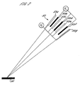
- a spectroscopic analyser 10 is shown in schematic detail.
- the analyser 10 is contained within a vacuum chamber 20 and a sample 30 of a material to be analysed is mounted within a sample holder (not shown) in the vacuum chamber 20.
- An irradiation source 40 is mounted onto the vacuum chamber 20 for irradiation of the sample 30.
- the spectroscopic analyser 10 of Figure 1 is configured in particular to allow either X-ray photoelectron spectroscopy or Auger electron spectroscopy.
- the irradiation source 40 generates a beam of X-rays which are directed on to the surface of the sample 30.
- a beam of electrons is instead directed at the surface of the sample 30.
- the incident radiation generates secondary electrons as described previously.
- the secondary electrons are emitted from the sample 30 in all directions.
- the gate 50 is capable of opening and closing, electronically, to the passage of the electron beam incident upon it at high speed.
- the gate 50 is, for most of the time, in the closed position, and opens for a very short period and then shuts again. This allows pulses, typically less than 1 nanosecond in duration, to be passed.
- the gate 50 is supplied with appropriate current or voltage to generate pulses of a suitable duration and duty cycle, using gate electronics 60.
- Gate electronics 60 are under the control of a central processor 80 as will be explained in further detail in connection with Figure 2.
- the electrons After passing through the gate, the electrons travel in a magnetic-field free flight tube 90, typically of one metre in length, before impinging upon an electron mirror 100. Accurate alignment of the electron optical axis of the system may be achieved by deflectors 110.
- the electron mirror 100 acts both to reflect and to focus electrons within the pulse, arriving from the gate 50, on to a detector 120.
- the detector is of conventional channel plate design, as employed in TOF mass analysers, but optimised for a fast pulse response with a rise time of typically less than 200 picoseconds. Suitable channel plates are manufactured by Burle Electronoptics, Inc. (USA), Hamamatsu Phototonics KK (Japan), and Photonis of France.
- Pulses arriving at the detector 120 are amplified by a pre-amplifier 130 and then passed to the histogramming TDC 70.
- the central processor 80 controls the gate electronics 60 and the histogramming TDC 70 so as to synchronise each. At the end of the data acquisition period, the histogrammed data is transferred to the central processor 80, which may, for example, be located in a personal computer, for further analysis.
- the spectroscopic analyser 10 is capable of operation over a wide range of energies. Nevertheless, when it is desired to acquire data of higher resolution over a narrow range of energies, it is possible to retard the secondary electrons emitted from the sample 30 before they arrive at the gate 50. This may be achieved, for example, by the use of a retarding mesh or lens 140. With this arrangement, the flight tube electron mirror 100 and the detector 120 are elevated to the retarding voltage applied to the retarding mesh or lens 140.
- the data acquired allows a measurement of energy to be made.
- the energy at which they are emitted remains broadly constant assuming that the vacuum chamber 20 and flight tube 90 are suitably evacuated.
- Synchronisation of the gate 50 and detector 20 means that the time of flight within the flight tube 90 can be used to calculate the energy of the emitted electron and hence surface analysis can be carried out.
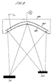
- the gate 50 is designed to open or close to the passage of the electron beam under the control of an applied voltage or current from the gate electronics 60. Most simply, the gating may be accomplished by the use of a retarding voltage which is greater than the maximum electron energy. However, it is more favourable to deflect the electrons from their normal flight path towards the gate into a trajectory where they can no longer reach the detector. One particularly preferred way of doing this, which minimises the voltage required to produce the necessary deflection, is shown in Figure 2.
- the gate 50 comprises a plurality of plates 55a-55g which are radially disposed from the sample 30.
- Alternate plates 55a, 55c, 55e and 55g are supplied with a drive voltage of a first polarity (in Figure 2, this is notionally labelled V+), and the remaining plates 55b, 55d and 55f are supplied with a voltage of the opposing polarity, notionally shown in Figure 2 as V-.
- the gate electronics 60 is arranged to supply these opposing polarity voltages.
- the first set of alternate plates 55a, 55c, 55e and 55g may be maintained at a ground potential and the remaining plates 55b, 55d and 55f may be connected to a single drive voltage of either the first or second polarity.
- the amplitude of the single drive voltage is approximately 2V (either 2V+ or 2V-).
- the gate 50 is controlled by the gate electronics 60 and, ultimately, by the central processor 80 to form pulses of a required pulse duration and duty cycle.
- the gate 50 is arranged to generate a single pulse, of typically less than 1 nanosecond duration with a pulse repetition period of typically 100 nanoseconds.
- the histogrammed data collected at the histogramming TDC 70 then represents the time-of-flight spectrum of the electrons generated from the sample.
- a pulse sequence is applied to the gate 50 instead of a series of single pulses.
- the preferred pulse sequence is known as a Hadamard sequence and further details of this may be found, for example, in "The Hadamard Transform" by P Treado and M Morris, Analytical Chemistry (1989) Volume 61, number 11, at pages 72A-734A.
- the histogrammed TOF signal from the detector 120 is transformed in software to reconstruct the original time-of-flight spectrum using a Hadamard transform, again as described in the above-referenced paper by Treado et al.
- Such a technique increases the duty cycle of the spectroscopic analyser 10 up to about 50%.
- the electron mirror 100 is required both to reflect and focus electrons over a wide energy range, as explained above. However, the mirror does not need to perform energy compensation as it would in an ion beam time-of-flight mass spectrometer. Whilst any suitable electrostatic or magnetic design may be employed (subject to these criteria), a particularly preferred embodiment of an electron mirror 100 is shown in Figure 3.
- a pair of concentric meshes 150, 160 are employed. Each mesh has a high transparency.
- the first mesh that is, the mesh closest to the gate 50 and detector 120
- the second concentric mesh 150 that is, the mesh furthest away from the gate 50 and detector 120
- the second concentric mesh 150 is biased to a negative voltage which is slightly larger than the maximum energy of interest.
- the meshes are toroidal or elliptical. However, for simplicity, the meshes may alternatively be spherical.
- An analogous mesh mirror design is used by Artamonov et al, in "An Application of the Electron Mirror in the Time-of-Flight Spectrometer", Journal of Electron Spectroscopy (2001), Volume 120, pages 11-26.
- spectroscopy which require the determination of the energy of electrons
- EELS Energy Electron Loss Spectroscopy
- LEELS Low Energy Electron Loss Spectroscopy
- UPS Ultraviolet Photoelectron Spectroscopy
Landscapes
- Chemical & Material Sciences (AREA)
- Analytical Chemistry (AREA)
- Analysing Materials By The Use Of Radiation (AREA)
Applications Claiming Priority (2)
| Application Number | Priority Date | Filing Date | Title |
|---|---|---|---|
| GB0209255A GB2390740A (en) | 2002-04-23 | 2002-04-23 | Spectroscopic analyser for surface analysis and method therefor |
| GB0209255 | 2002-04-23 |
Publications (2)
| Publication Number | Publication Date |
|---|---|
| EP1357578A2 true EP1357578A2 (fr) | 2003-10-29 |
| EP1357578A3 EP1357578A3 (fr) | 2005-04-06 |
Family
ID=9935344
Family Applications (1)
| Application Number | Title | Priority Date | Filing Date |
|---|---|---|---|
| EP03252540A Withdrawn EP1357578A3 (fr) | 2002-04-23 | 2003-04-23 | Dispositif et méthode pour l' analyse de surface par spectroscopie |
Country Status (3)
| Country | Link |
|---|---|
| US (1) | US20040021069A1 (fr) |
| EP (1) | EP1357578A3 (fr) |
| GB (1) | GB2390740A (fr) |
Cited By (1)
| Publication number | Priority date | Publication date | Assignee | Title |
|---|---|---|---|---|
| WO2009137706A3 (fr) * | 2008-05-08 | 2010-02-25 | Kla-Tencor Corporation | Spectroscopie différentielle in situ |
Families Citing this family (3)
| Publication number | Priority date | Publication date | Assignee | Title |
|---|---|---|---|---|
| GB0700754D0 (en) * | 2007-01-15 | 2007-02-21 | Oxford Instr Analytical Ltd | Charged particle analyser and method |
| FR2942349B1 (fr) * | 2009-02-13 | 2012-04-27 | Cameca | Dispositif d'analyse de masse a large acceptance angulaire comprenant un reflectron |
| US8642951B2 (en) * | 2011-05-04 | 2014-02-04 | Agilent Technologies, Inc. | Device, system, and method for reflecting ions |
Family Cites Families (18)
| Publication number | Priority date | Publication date | Assignee | Title |
|---|---|---|---|---|
| US3435207A (en) * | 1966-01-06 | 1969-03-25 | Gen Electric | Apparatus for measuring velocity of low energy electrons |
| US3582648A (en) * | 1968-06-05 | 1971-06-01 | Varian Associates | Electron impact time of flight spectrometer |
| US5159195A (en) * | 1987-11-09 | 1992-10-27 | The University Of Michigan | Position microscopy |
| JP2590417B2 (ja) * | 1992-06-19 | 1997-03-12 | 工業技術院長 | オージェ電子分光装置 |
| US5569916A (en) * | 1992-07-09 | 1996-10-29 | Agency Of Industrial Science & Technology, Ministry Of International Trade & Industry | Electron spectroscopy apparatus |
| GB9220097D0 (en) * | 1992-09-23 | 1992-11-04 | Univ York | Electron spectrometers |
| JPH06275228A (ja) * | 1993-03-23 | 1994-09-30 | Anelva Corp | ダスト分析装置及びダスト分析方法 |
| JPH07280755A (ja) * | 1994-04-15 | 1995-10-27 | Hitachi Ltd | 表面解析方法 |
| GB9510699D0 (en) * | 1995-05-26 | 1995-07-19 | Fisons Plc | Apparatus and method for surface analysis |
| GB9617312D0 (en) * | 1996-08-17 | 1996-09-25 | Millbrook Instr Limited | Charged particle velocity analyser |
| AUPO557797A0 (en) * | 1997-03-12 | 1997-04-10 | Gbc Scientific Equipment Pty Ltd | A time of flight analysis device |
| JPH1123499A (ja) * | 1997-07-03 | 1999-01-29 | Nikon Corp | 電子分光法 |
| US6326617B1 (en) * | 1997-09-04 | 2001-12-04 | Synaptic Pharmaceutical Corporation | Photoelectron spectroscopy apparatus |
| US5969354A (en) * | 1997-12-09 | 1999-10-19 | Kelly; Michael A. | Electron analyzer with integrated optics |
| GB9800488D0 (en) * | 1998-01-12 | 1998-03-04 | Univ York | Electron energy analyser |
| US6348688B1 (en) * | 1998-02-06 | 2002-02-19 | Perseptive Biosystems | Tandem time-of-flight mass spectrometer with delayed extraction and method for use |
| US6300626B1 (en) * | 1998-08-17 | 2001-10-09 | Board Of Trustees Of The Leland Stanford Junior University | Time-of-flight mass spectrometer and ion analysis |
| US6674069B1 (en) * | 1998-12-17 | 2004-01-06 | Jeol Usa, Inc. | In-line reflecting time-of-flight mass spectrometer for molecular structural analysis using collision induced dissociation |
-
2002
- 2002-04-23 GB GB0209255A patent/GB2390740A/en not_active Withdrawn
-
2003
- 2003-04-23 US US10/421,676 patent/US20040021069A1/en not_active Abandoned
- 2003-04-23 EP EP03252540A patent/EP1357578A3/fr not_active Withdrawn
Cited By (1)
| Publication number | Priority date | Publication date | Assignee | Title |
|---|---|---|---|---|
| WO2009137706A3 (fr) * | 2008-05-08 | 2010-02-25 | Kla-Tencor Corporation | Spectroscopie différentielle in situ |
Also Published As
| Publication number | Publication date |
|---|---|
| GB2390740A (en) | 2004-01-14 |
| GB0209255D0 (en) | 2002-06-05 |
| US20040021069A1 (en) | 2004-02-05 |
| EP1357578A3 (fr) | 2005-04-06 |
Similar Documents
| Publication | Publication Date | Title |
|---|---|---|
| Vanbellingen et al. | Time‐of‐flight secondary ion mass spectrometry imaging of biological samples with delayed extraction for high mass and high spatial resolutions | |
| Oelsner et al. | Microspectroscopy and imaging using a delay line detector in time-of-flight photoemission microscopy | |
| JP3801866B2 (ja) | 飛行時間型質量分析計 | |
| US5032722A (en) | MS-MS time-of-flight mass spectrometer | |
| JP5723893B2 (ja) | 質量分析計およびイオン分離検出方法 | |
| US20130126727A1 (en) | Time-of-Flight Electron Energy Analyzer | |
| JPH07500448A (ja) | 分解能と伝達効率との間の性能配分を可能とする開口を備えた飛行時間型質量分析計 | |
| US5650616A (en) | Apparatus and method for analyzing surface | |
| Myers et al. | An inductively coupled plasma-time-of-flight mass spectrometer for elemental analysis. Part II: Direct current quadrupole lens system for improved performance | |
| US5665967A (en) | Apparatus and method for surface analysis | |
| WO2011066551A1 (fr) | Spectrométrie à temps de vol et spectroscopie de surfaces | |
| US6984821B1 (en) | Mass spectrometer and methods of increasing dispersion between ion beams | |
| JP2567736B2 (ja) | イオン散乱分析装置 | |
| CN112305002A (zh) | 光谱学和成像系统 | |
| JPS6229049A (ja) | 質量分析計 | |
| JP7555428B2 (ja) | 高性能荷電粒子検出のための装置および方法 | |
| US4889987A (en) | Photo ion spectrometer | |
| JP3392345B2 (ja) | 飛行時間型質量分析装置 | |
| JP5504969B2 (ja) | 質量分析装置 | |
| US5026988A (en) | Method and apparatus for time of flight medium energy particle scattering | |
| EP1357578A2 (fr) | Dispositif et méthode pour l' analyse de surface par spectroscopie | |
| Kugeler et al. | Calculation and measurement of the time-of-flight spread in a hemispherical electron energy analyzer | |
| Prümper et al. | Combining high mass resolution and velocity imaging in a time-of-flight ion spectrometer using pulsed fields and an electrostatic lens | |
| JP7528191B2 (ja) | 焦点面検出器 | |
| JP2764505B2 (ja) | 電子分光方法とこれを用いた電子分光装置 |
Legal Events
| Date | Code | Title | Description |
|---|---|---|---|
| PUAI | Public reference made under article 153(3) epc to a published international application that has entered the european phase |
Free format text: ORIGINAL CODE: 0009012 |
|
| AK | Designated contracting states |
Kind code of ref document: A2 Designated state(s): AT BE BG CH CY CZ DE DK EE ES FI FR GB GR HU IE IT LI LU MC NL PT RO SE SI SK TR |
|
| AX | Request for extension of the european patent |
Extension state: AL LT LV MK |
|
| PUAL | Search report despatched |
Free format text: ORIGINAL CODE: 0009013 |
|
| AK | Designated contracting states |
Kind code of ref document: A3 Designated state(s): AT BE BG CH CY CZ DE DK EE ES FI FR GB GR HU IE IT LI LU MC NL PT RO SE SI SK TR |
|
| AX | Request for extension of the european patent |
Extension state: AL LT LV MK |
|
| RIC1 | Information provided on ipc code assigned before grant |
Ipc: 7H 01J 49/44 B Ipc: 7H 01J 49/40 A |
|
| AKX | Designation fees paid | ||
| REG | Reference to a national code |
Ref country code: DE Ref legal event code: 8566 |
|
| STAA | Information on the status of an ep patent application or granted ep patent |
Free format text: STATUS: THE APPLICATION IS DEEMED TO BE WITHDRAWN |
|
| 18D | Application deemed to be withdrawn |
Effective date: 20051007 |