EP1359629A2 - Stabile elektrolumineszente Vorrichtung - Google Patents
Stabile elektrolumineszente Vorrichtung Download PDFInfo
- Publication number
- EP1359629A2 EP1359629A2 EP03076077A EP03076077A EP1359629A2 EP 1359629 A2 EP1359629 A2 EP 1359629A2 EP 03076077 A EP03076077 A EP 03076077A EP 03076077 A EP03076077 A EP 03076077A EP 1359629 A2 EP1359629 A2 EP 1359629A2
- Authority
- EP
- European Patent Office
- Prior art keywords
- stabilizer
- layer
- sample
- host
- compound
- Prior art date
- Legal status (The legal status is an assumption and is not a legal conclusion. Google has not performed a legal analysis and makes no representation as to the accuracy of the status listed.)
- Withdrawn
Links
- 0 c(cc1C(C=C2c3ccccc33)=*4*5(*67)*2*3=C2)ccc1C4=CC6=C(C=CC=C1)C1=C7C=C1*5=C2c2ccccc12 Chemical compound c(cc1C(C=C2c3ccccc33)=*4*5(*67)*2*3=C2)ccc1C4=CC6=C(C=CC=C1)C1=C7C=C1*5=C2c2ccccc12 0.000 description 2
- JVHCQVUVHZFKLQ-UHFFFAOYSA-N c(ccc1c(-c2cccnc2)c2c3)cc1cc2cc-1c3-c2ccc-3c4c2c-1ccc4-c1c2c-3cccc2ccc1 Chemical compound c(ccc1c(-c2cccnc2)c2c3)cc1cc2cc-1c3-c2ccc-3c4c2c-1ccc4-c1c2c-3cccc2ccc1 JVHCQVUVHZFKLQ-UHFFFAOYSA-N 0.000 description 1
Images
Classifications
-
- H—ELECTRICITY
- H05—ELECTRIC TECHNIQUES NOT OTHERWISE PROVIDED FOR
- H05B—ELECTRIC HEATING; ELECTRIC LIGHT SOURCES NOT OTHERWISE PROVIDED FOR; CIRCUIT ARRANGEMENTS FOR ELECTRIC LIGHT SOURCES, IN GENERAL
- H05B33/00—Electroluminescent light sources
- H05B33/12—Light sources with substantially two-dimensional [2D] radiating surfaces
- H05B33/18—Light sources with substantially two-dimensional [2D] radiating surfaces characterised by the nature or concentration of the activator
-
- C—CHEMISTRY; METALLURGY
- C09—DYES; PAINTS; POLISHES; NATURAL RESINS; ADHESIVES; COMPOSITIONS NOT OTHERWISE PROVIDED FOR; APPLICATIONS OF MATERIALS NOT OTHERWISE PROVIDED FOR
- C09K—MATERIALS FOR MISCELLANEOUS APPLICATIONS, NOT PROVIDED FOR ELSEWHERE
- C09K11/00—Luminescent materials, e.g. electroluminescent or chemiluminescent
- C09K11/06—Luminescent materials, e.g. electroluminescent or chemiluminescent containing organic luminescent materials
-
- H—ELECTRICITY
- H10—SEMICONDUCTOR DEVICES; ELECTRIC SOLID-STATE DEVICES NOT OTHERWISE PROVIDED FOR
- H10K—ORGANIC ELECTRIC SOLID-STATE DEVICES
- H10K50/00—Organic light-emitting devices
- H10K50/10—OLEDs or polymer light-emitting diodes [PLED]
- H10K50/11—OLEDs or polymer light-emitting diodes [PLED] characterised by the electroluminescent [EL] layers
- H10K50/12—OLEDs or polymer light-emitting diodes [PLED] characterised by the electroluminescent [EL] layers comprising dopants
-
- H—ELECTRICITY
- H10—SEMICONDUCTOR DEVICES; ELECTRIC SOLID-STATE DEVICES NOT OTHERWISE PROVIDED FOR
- H10K—ORGANIC ELECTRIC SOLID-STATE DEVICES
- H10K85/00—Organic materials used in the body or electrodes of devices covered by this subclass
- H10K85/60—Organic compounds having low molecular weight
- H10K85/615—Polycyclic condensed aromatic hydrocarbons, e.g. anthracene
- H10K85/624—Polycyclic condensed aromatic hydrocarbons, e.g. anthracene containing six or more rings
-
- C—CHEMISTRY; METALLURGY
- C09—DYES; PAINTS; POLISHES; NATURAL RESINS; ADHESIVES; COMPOSITIONS NOT OTHERWISE PROVIDED FOR; APPLICATIONS OF MATERIALS NOT OTHERWISE PROVIDED FOR
- C09K—MATERIALS FOR MISCELLANEOUS APPLICATIONS, NOT PROVIDED FOR ELSEWHERE
- C09K2211/00—Chemical nature of organic luminescent or tenebrescent compounds
- C09K2211/10—Non-macromolecular compounds
- C09K2211/1003—Carbocyclic compounds
- C09K2211/1011—Condensed systems
-
- C—CHEMISTRY; METALLURGY
- C09—DYES; PAINTS; POLISHES; NATURAL RESINS; ADHESIVES; COMPOSITIONS NOT OTHERWISE PROVIDED FOR; APPLICATIONS OF MATERIALS NOT OTHERWISE PROVIDED FOR
- C09K—MATERIALS FOR MISCELLANEOUS APPLICATIONS, NOT PROVIDED FOR ELSEWHERE
- C09K2211/00—Chemical nature of organic luminescent or tenebrescent compounds
- C09K2211/10—Non-macromolecular compounds
- C09K2211/1003—Carbocyclic compounds
- C09K2211/1014—Carbocyclic compounds bridged by heteroatoms, e.g. N, P, Si or B
-
- C—CHEMISTRY; METALLURGY
- C09—DYES; PAINTS; POLISHES; NATURAL RESINS; ADHESIVES; COMPOSITIONS NOT OTHERWISE PROVIDED FOR; APPLICATIONS OF MATERIALS NOT OTHERWISE PROVIDED FOR
- C09K—MATERIALS FOR MISCELLANEOUS APPLICATIONS, NOT PROVIDED FOR ELSEWHERE
- C09K2211/00—Chemical nature of organic luminescent or tenebrescent compounds
- C09K2211/10—Non-macromolecular compounds
- C09K2211/1018—Heterocyclic compounds
- C09K2211/1025—Heterocyclic compounds characterised by ligands
-
- C—CHEMISTRY; METALLURGY
- C09—DYES; PAINTS; POLISHES; NATURAL RESINS; ADHESIVES; COMPOSITIONS NOT OTHERWISE PROVIDED FOR; APPLICATIONS OF MATERIALS NOT OTHERWISE PROVIDED FOR
- C09K—MATERIALS FOR MISCELLANEOUS APPLICATIONS, NOT PROVIDED FOR ELSEWHERE
- C09K2211/00—Chemical nature of organic luminescent or tenebrescent compounds
- C09K2211/18—Metal complexes
- C09K2211/183—Metal complexes of the refractory metals, i.e. Ti, V, Cr, Zr, Nb, Mo, Hf, Ta or W
-
- C—CHEMISTRY; METALLURGY
- C09—DYES; PAINTS; POLISHES; NATURAL RESINS; ADHESIVES; COMPOSITIONS NOT OTHERWISE PROVIDED FOR; APPLICATIONS OF MATERIALS NOT OTHERWISE PROVIDED FOR
- C09K—MATERIALS FOR MISCELLANEOUS APPLICATIONS, NOT PROVIDED FOR ELSEWHERE
- C09K2211/00—Chemical nature of organic luminescent or tenebrescent compounds
- C09K2211/18—Metal complexes
- C09K2211/187—Metal complexes of the iron group metals, i.e. Fe, Co or Ni
-
- C—CHEMISTRY; METALLURGY
- C09—DYES; PAINTS; POLISHES; NATURAL RESINS; ADHESIVES; COMPOSITIONS NOT OTHERWISE PROVIDED FOR; APPLICATIONS OF MATERIALS NOT OTHERWISE PROVIDED FOR
- C09K—MATERIALS FOR MISCELLANEOUS APPLICATIONS, NOT PROVIDED FOR ELSEWHERE
- C09K2211/00—Chemical nature of organic luminescent or tenebrescent compounds
- C09K2211/18—Metal complexes
- C09K2211/188—Metal complexes of other metals not provided for in one of the previous groups
-
- H—ELECTRICITY
- H10—SEMICONDUCTOR DEVICES; ELECTRIC SOLID-STATE DEVICES NOT OTHERWISE PROVIDED FOR
- H10K—ORGANIC ELECTRIC SOLID-STATE DEVICES
- H10K2101/00—Properties of the organic materials covered by group H10K85/00
- H10K2101/10—Triplet emission
-
- H—ELECTRICITY
- H10—SEMICONDUCTOR DEVICES; ELECTRIC SOLID-STATE DEVICES NOT OTHERWISE PROVIDED FOR
- H10K—ORGANIC ELECTRIC SOLID-STATE DEVICES
- H10K50/00—Organic light-emitting devices
- H10K50/10—OLEDs or polymer light-emitting diodes [PLED]
- H10K50/11—OLEDs or polymer light-emitting diodes [PLED] characterised by the electroluminescent [EL] layers
-
- H—ELECTRICITY
- H10—SEMICONDUCTOR DEVICES; ELECTRIC SOLID-STATE DEVICES NOT OTHERWISE PROVIDED FOR
- H10K—ORGANIC ELECTRIC SOLID-STATE DEVICES
- H10K85/00—Organic materials used in the body or electrodes of devices covered by this subclass
- H10K85/30—Coordination compounds
- H10K85/311—Phthalocyanine
-
- H—ELECTRICITY
- H10—SEMICONDUCTOR DEVICES; ELECTRIC SOLID-STATE DEVICES NOT OTHERWISE PROVIDED FOR
- H10K—ORGANIC ELECTRIC SOLID-STATE DEVICES
- H10K85/00—Organic materials used in the body or electrodes of devices covered by this subclass
- H10K85/30—Coordination compounds
- H10K85/341—Transition metal complexes, e.g. Ru(II)polypyridine complexes
- H10K85/342—Transition metal complexes, e.g. Ru(II)polypyridine complexes comprising iridium
-
- H—ELECTRICITY
- H10—SEMICONDUCTOR DEVICES; ELECTRIC SOLID-STATE DEVICES NOT OTHERWISE PROVIDED FOR
- H10K—ORGANIC ELECTRIC SOLID-STATE DEVICES
- H10K85/00—Organic materials used in the body or electrodes of devices covered by this subclass
- H10K85/30—Coordination compounds
- H10K85/341—Transition metal complexes, e.g. Ru(II)polypyridine complexes
- H10K85/346—Transition metal complexes, e.g. Ru(II)polypyridine complexes comprising platinum
-
- H—ELECTRICITY
- H10—SEMICONDUCTOR DEVICES; ELECTRIC SOLID-STATE DEVICES NOT OTHERWISE PROVIDED FOR
- H10K—ORGANIC ELECTRIC SOLID-STATE DEVICES
- H10K85/00—Organic materials used in the body or electrodes of devices covered by this subclass
- H10K85/60—Organic compounds having low molecular weight
- H10K85/615—Polycyclic condensed aromatic hydrocarbons, e.g. anthracene
- H10K85/622—Polycyclic condensed aromatic hydrocarbons, e.g. anthracene containing four rings, e.g. pyrene
-
- H—ELECTRICITY
- H10—SEMICONDUCTOR DEVICES; ELECTRIC SOLID-STATE DEVICES NOT OTHERWISE PROVIDED FOR
- H10K—ORGANIC ELECTRIC SOLID-STATE DEVICES
- H10K85/00—Organic materials used in the body or electrodes of devices covered by this subclass
- H10K85/60—Organic compounds having low molecular weight
- H10K85/615—Polycyclic condensed aromatic hydrocarbons, e.g. anthracene
- H10K85/623—Polycyclic condensed aromatic hydrocarbons, e.g. anthracene containing five rings, e.g. pentacene
-
- H—ELECTRICITY
- H10—SEMICONDUCTOR DEVICES; ELECTRIC SOLID-STATE DEVICES NOT OTHERWISE PROVIDED FOR
- H10K—ORGANIC ELECTRIC SOLID-STATE DEVICES
- H10K85/00—Organic materials used in the body or electrodes of devices covered by this subclass
- H10K85/60—Organic compounds having low molecular weight
- H10K85/631—Amine compounds having at least two aryl rest on at least one amine-nitrogen atom, e.g. triphenylamine
-
- H—ELECTRICITY
- H10—SEMICONDUCTOR DEVICES; ELECTRIC SOLID-STATE DEVICES NOT OTHERWISE PROVIDED FOR
- H10K—ORGANIC ELECTRIC SOLID-STATE DEVICES
- H10K85/00—Organic materials used in the body or electrodes of devices covered by this subclass
- H10K85/60—Organic compounds having low molecular weight
- H10K85/649—Aromatic compounds comprising a hetero atom
- H10K85/652—Cyanine dyes
-
- H—ELECTRICITY
- H10—SEMICONDUCTOR DEVICES; ELECTRIC SOLID-STATE DEVICES NOT OTHERWISE PROVIDED FOR
- H10K—ORGANIC ELECTRIC SOLID-STATE DEVICES
- H10K85/00—Organic materials used in the body or electrodes of devices covered by this subclass
- H10K85/60—Organic compounds having low molecular weight
- H10K85/649—Aromatic compounds comprising a hetero atom
- H10K85/653—Aromatic compounds comprising a hetero atom comprising only oxygen as heteroatom
-
- H—ELECTRICITY
- H10—SEMICONDUCTOR DEVICES; ELECTRIC SOLID-STATE DEVICES NOT OTHERWISE PROVIDED FOR
- H10K—ORGANIC ELECTRIC SOLID-STATE DEVICES
- H10K85/00—Organic materials used in the body or electrodes of devices covered by this subclass
- H10K85/60—Organic compounds having low molecular weight
- H10K85/649—Aromatic compounds comprising a hetero atom
- H10K85/656—Aromatic compounds comprising a hetero atom comprising two or more different heteroatoms per ring
-
- H—ELECTRICITY
- H10—SEMICONDUCTOR DEVICES; ELECTRIC SOLID-STATE DEVICES NOT OTHERWISE PROVIDED FOR
- H10K—ORGANIC ELECTRIC SOLID-STATE DEVICES
- H10K85/00—Organic materials used in the body or electrodes of devices covered by this subclass
- H10K85/60—Organic compounds having low molecular weight
- H10K85/649—Aromatic compounds comprising a hetero atom
- H10K85/657—Polycyclic condensed heteroaromatic hydrocarbons
-
- Y—GENERAL TAGGING OF NEW TECHNOLOGICAL DEVELOPMENTS; GENERAL TAGGING OF CROSS-SECTIONAL TECHNOLOGIES SPANNING OVER SEVERAL SECTIONS OF THE IPC; TECHNICAL SUBJECTS COVERED BY FORMER USPC CROSS-REFERENCE ART COLLECTIONS [XRACs] AND DIGESTS
- Y10—TECHNICAL SUBJECTS COVERED BY FORMER USPC
- Y10S—TECHNICAL SUBJECTS COVERED BY FORMER USPC CROSS-REFERENCE ART COLLECTIONS [XRACs] AND DIGESTS
- Y10S428/00—Stock material or miscellaneous articles
- Y10S428/917—Electroluminescent
Definitions
- This invention relates to organic light emitting diode-containing devices comprising a light emitting layer that contains a stabilizer that improves the operating stability of the device.
- an organic EL device is comprised of an anode for hole injection, a cathode for electron injection, and an organic medium sandwiched between these electrodes to support charge recombination that yields emission of light. These devices are also commonly referred to as organic light-emitting diodes, or OLEDs.
- organic EL devices are Gurnee et al. U.S. Pat. No. 3,172,862, issued Mar. 9, 1965; Gurnee U.S. Pat. No. 3,173,050, issued Mar.
- More recent organic EL devices include an organic EL element consisting of extremely thin layers (e.g. ⁇ 1.0 ⁇ m ) between the anode and the cathode.
- the organic EL element encompasses the layers between the anode and cathode electrodes. Reducing the thickness lowered the resistance of the organic layer and has enabled devices that operate at much lower voltage.
- one organic layer of the EL element adjacent to the anode is specifically chosen to transport holes, therefore, it is referred to as the hole-transporting layer, and the other organic layer is specifically chosen to transport electrons, referred to as the electron-transporting layer.
- the interface between the two layers provides an efficient site for the recombination of the injected hole/electron pair and the resultant electroluminescence.
- the light-emitting layer commonly consists of a host material doped with a guest material - dopant, which results in an efficiency improvement and allows color tuning.
- the invention provides an OLED device comprising an anode and a cathode and, located therebetween, a light emitting layer (LEL) containing a host and a stabilizer, wherein the stabilizer contains at least 5 fused rings and exhibits a first triplet energy level below 130 kJ/mol.
- LEL light emitting layer
- the invention also provides an imaging or illuminating device including the OLED device and a process for forming an image using the OLED device.
- the OLED deviceof the invention contains a light emitting layer exhibiting improved operational stability.
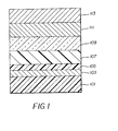
- FIG. 1 shows a cross-section of a typical OLED device in which this invention may be used.
- An OLED device of the invention is a multilayer electroluminescent device comprising a cathode, an anode, charge-injecting layers (if necessary), charge-transporting layers, and a light-emitting layer (LEL) comprising a host and at least one stabilizer, where the stabilizer contains at least 5 fused rings and exhibits a first triplet state energy level below 130 kJ/mol.
- LEL light-emitting layer
- the light-emitting layer of the device also contains a dopant, where the dopant is present in an amount of up to 10 wt % of the host, more typically from 0.1-5.0 wt % of the host.
- Stabilizer is defined as organic material which can increase the operational lifetime of the OLED device when present in an amount of up to 95 wt % of the host.
- the increase in operational lifetime or half-life is relative to the situation where the stabilizer is absent.
- Operational lifetime is commonly defined as the time to reach half of the initial luminance at a given temperature and current density.
- the dopant and stabilizer materials are different. It is further preferred that that the emissive molecule and stabilizer molecule are different.
- Stabilizers useful in the invention are suitably selected from organic molecules containing at least 5 fused rings and exhibiting the first triplet state energy below 130 kJ/mol. Most chemical species in the lowest energy state are singlets, which means that all electrons are paired and total spin is 0. If two electrons are unpaired with parallel spin, the total spin is 1 and the species is said to be in triplet state.
- the first triplet state energy is the difference in energy between the ground state and the lowest triplet state of the molecule and can be determined by various spectroscopic techniques including singlet-triplet excitation and emission spectra. Alternatively, the first triplet state energy can also be calculated using quantum chemistry methods, particularly hybrid density-functional theory.
- stabilizer molecules By the introduction of stabilizer molecules into an OLED device, we expect to convert triplet states formed by electrical excitation into triplet states of the stabilizer molecules characterized by substantially lower energies, faster conversion to the respective ground states and, consequently, lower probability of initiating undesirable chemical reactions that result in shortening operational lifetime of an OLED device.
- the stabilizer useful in the invention may be suitably selected from organic molecules containing at least 5 fused rings and exhibiting the first triplet state energy below 130 kJ/mol. The energy may be measured spectroscopically or calculated with unrestricted B3LYP/6-31G* method as a difference between energies of equilibrium geometries of the ground and the lowest triplet state.
- Triplet state energies were obtained experimentally or calculated as differences between the lowest energy singlet state (ground state) and the lowest energy triplet state.
- the stabilizer may be selected from hydrocarbons, heteroaromatic compounds, and metal complexes. These compounds may also contain one or more suitable substituents as long as the substituent does not destroy properties necessary for device utility.
- the stabilizer is suitably present in an amount sufficient to improve the stability of the device by prolonging the half-life by at least 100%, desirably at lest 200%, compared to the same LEL without the stabilizer.
- the OLED device comprises a light-emitting layer containing a host, an emissive dopant, and a stabilizer, wherein the stabilizer contains at least 5 fused rings and is selected from the group consisting of a phthalocyanine compound, an indenoperylene compound and an arylpyrene compound. Particularly useful is copper phthalocyanine.
- Useful emissive dopants include a phosphorescent dye or a fluorescent dye selected from anthracene, tetracene, xanthene, perylene, rubrene, coumarin, rhodamine, quinacridone, dicyanomethylenepyran, thiopyran, polymethine, pyrilium thiapyrilium, and carbostyryl compounds.
- Useful hosts include a chelated oxinoid compound, a dicarbazole-biphenyl compound such as 4,4'- N , N '-dicarbazole-1,1'-biphenyl (CBP), and an anthracene compound such as 2- tert -butyl-9,10-di-(2-naphthyl)anthracene.
- a chelated oxinoid compound such as 4,4'- N , N '-dicarbazole-1,1'-biphenyl (CBP)
- anthracene compound such as 2- tert -butyl-9,10-di-(2-naphthyl)anthracene.
- One group of compounds useful in the invention is a stabilizer that contains at least 5 fused rings and is represented by Formula (1): wherein, each X a , X b , X c , X d is an independently selected substituent, two of which may join to form a fused ring and k, l, m, and n are independently 0 to 4; each Y a , Y b , Y c , Y d is independently selected as either carbon or nitrogen atoms and X e , X f , X g , X h exist only in cases of carbon atoms; each X e , X f , X g , X h is hydrogen or an independently selected substituent; X i is a substituent and o is 0-2; and M is metal or metalloid atom.
- each X a , X b , X c , X d is an independently selected substituent, two of
- the compound of Formula (1) is symmetric.
- Two of X a , X b , X c and X d are suitably joined to form a ring.
- Convenient substituents for X a , X b , X c and X d are alkyl, alkoxy, aryl, and halogen groups but usually, k, l, m, and n are 0.
- Y a , Y b , Y c , and Y d are either all carbon or all nitrogen atoms, with all nitrogen being useful.
- X e , X f , X g , and X h are suitably an alkyl or aryl group. Typically, o is 0.
- M is a multivalent metal such as a transition metal, especially cobalt or copper.
- stabilizer materials are the following. These compounds may also contain one or more suitable substituents as long as the substituent does not destroy properties necessary for device utility.
- an imaging device including the OLED device, an illuminating device including the OLED device, and a process for forming an image employing the OLED device of the invention.
- substituted or “substituent” means any group or atom other than hydrogen (what about deuterium).
- group when the term “group” is used, it means that when a substituent group contains a substitutable hydrogen, it is also intended to encompass not only the substituent's unsubstituted form, but also its form further substituted with any substituent group or groups as herein mentioned, so long as the substituent does not destroy properties necessary for device utility.
- a substituent group may be halogen or may be bonded to the remainder of the molecule by an atom of carbon, silicon, oxygen, nitrogen, phosphorous, sulfur, selenium, or boron.
- the substituent may be, for example, halogen, such as chloro, bromo or fluoro; oxo; nitro; hydroxyl; cyano; carboxyl; or groups which may be further substituted, such as alkyl, including straight or branched chain or cyclic alkyl, such as methyl, trifluoromethyl, ethyl, t -butyl, 3-(2,4-di- t -pentylphenoxy) propyl, and tetradecyl; alkenyl, such as ethylene, 2-butene; alkoxy, such as methoxy, ethoxy, propoxy, butoxy, 2-methoxyethoxy, sec -butoxy, hexyloxy, 2-ethylhexyloxy, tetradecyloxy, 2-(2,4-di- t -pentylphenoxy)ethoxy, and 2-dodecyloxyethoxy; aryl such as pheny
- quaternary ammonium such as triethylammonium
- quaternary phosphonium such as triphenylphosphonium
- silyloxy such as trimethylsilyloxy.
- the substituents may themselves be further substituted one or more times with the described substituent groups.
- the particular substituents used may be selected by those skilled in the art to attain the desired desirable properties for a specific application and can include, for example, electron-withdrawing groups, electron-donating groups, and steric groups.
- the substituents may be joined together to form a ring such as a fused ring unless otherwise provided.
- the above groups and substituents thereof may include those having up to 48 carbon atoms, typically 1 to 36 carbon atoms and usually less than 24 carbon atoms, but greater numbers are possible depending on the particular substituents selected.
- the present invention can be employed in most OLED device configurations. These include very simple structures comprising a single anode and cathode to more complex devices, such as passive matrix displays comprised of orthogonal arrays of anodes and cathodes to form pixels, and active-matrix displays where each pixel is controlled independently, for example, with a thin film transistor (TFT).
- TFT thin film transistor
- FIG. 1 A more typical structure is shown in Figure 1 and contains a substrate 101 , an anode 103 , an optional hole-injecting layer 105 , a hole-transporting layer 107 , a light-emitting layer 109 , an electron-transporting layer 111 , and a cathode 113 . These layers are described in detail below. Note that the substrate may alternatively be located adjacent to the cathode, or the substrate may actually constitute the anode or cathode. Also, the total combined thickness of the organic layers is preferably less than 500 nm.
- the substrate 101 can either be light transmissive or opaque, depending on the intended direction of light emission.
- the light transmissive property is desirable for viewing the EL emission through the substrate.
- Transparent glass or organic material are commonly employed in such cases.
- the transmissive characteristic of the bottom support is immaterial, and therefore can be light transmissive, light absorbing or light reflective.
- Substrates for use in this case include, but are not limited to, glass, plastic, semiconductor materials, ceramics, and circuit board materials. Of course it is necessary to provide in these device configurations a light-transparent top electrode.
- the conductive anode layer 103 is commonly formed over the substrate and, when EL emission is viewed through the anode, should be transparent or substantially transparent to the emission of interest.
- Common transparent anode materials used in this invention are indium-tin oxide (ITO) and tin oxide, but other metal oxides can work including, but not limited to, aluminum- or indium-doped zinc oxide (IZO), magnesium-indium oxide, and nickel-tungsten oxide.
- ITO indium-tin oxide
- IZO aluminum- or indium-doped zinc oxide
- IZO aluminum- or indium-doped zinc oxide
- nickel-tungsten oxide nickel-tungsten oxide.
- metal nitrides such as gallium nitride
- metal selenides such as zinc selenide
- metal sulfides such as zinc sulfide
- the transmissive characteristics of layer 103 are immaterial and any conductive material can be used, transparent, opaque or reflective.
- Example conductors for this application include, but are not limited to, gold, iridium, molybdenum, palladium, and platinum.
- Typical anode materials, transmissive or otherwise, have a work function of 4.1 eV or greater. Desired anode materials are commonly deposited by any suitable means such as evaporation, sputtering, chemical vapor deposition, or electrochemical means. Anodes can be patterned using well-known photolithographic processes.
- HIL Hole-Injecting Layer
- a hole-injecting layer 105 be provided between anode 103 and hole-transporting layer 107 .
- the hole-injecting material can serve to improve the film formation property of subsequent organic layers and to facilitate injection of holes into the hole-transporting layer.
- Suitable materials for use in the hole-injecting layer include, but are not limited to, porphyrinic compounds such as those described in US 4,720,432, and plasma-deposited fluorocarbon polymers such as those described in US 6,208,075.
- Alternative hole-injecting materials reportedly useful in organic EL devices are described in EP 0 891 121 A1 and EP 1 029 909 A1.
- HTL Hole-Transporting Layer
- the hole-transporting layer 107 of the organic EL device contains at least one hole-transporting compound such as an aromatic tertiary amine, where the latter is understood to be a compound containing at least one trivalent nitrogen atom that is bonded only to carbon atoms, at least one of which is a member of an aromatic ring.
- the aromatic tertiary amine can be an arylamine, such as a monoarylamine, diarylamine, triarylamine, or a polymeric arylamine group. Exemplary monomeric triarylamines are illustrated by Klupfel et al. US 3,180,730.
- Other suitable triarylamines substituted with one or more vinyl radicals and/or comprising at least one active hydrogen containing group are disclosed by Brantley et al US 3,567,450 and US 3,658,520.
- a more preferred class of aromatic tertiary amines are those which include at least two aromatic tertiary amine moieties as described in US 4,720,432 and US 5,061,569.
- Such compounds include those represented by structural formula (A). wherein Q 1 and Q 2 are independently selected aromatic tertiary amine moieties and G is a linking group such as an arylene, cycloalkylene, or alkylene group of a carbon to carbon bond.
- at least one of Q 1 or Q 2 contains a polycyclic fused ring group, e.g., a naphthalene.
- G is an aryl group, it is conveniently a phenylene, biphenylene, or naphthalene group.
- a useful class of triarylamine groups satisfying structural formula (A) and containing two triarylamine groups is represented by structural formula (B): where R 1 and R 2 each independently represents a hydrogen atom, an aryl group, or an alkyl group or R 1 and R 2 together represent the atoms completing a cycloalkyl group; and R 3 and R 4 each independently represents an aryl group, which is in turn substituted with a diaryl substituted amino group, as indicated by structural formula (C): wherein R 5 and R 6 are independently selected aryl groups.
- at least one of R 5 or R 6 contains a polycyclic fused ring group, e.g., a naphthalene.
- tetraaryldiamines Another class of aromatic tertiary amine groups are the tetraaryldiamines. Desirable tetraaryldiamines groups include two diarylamino groups, such as indicated by formula (C), linked through an arylene group. Useful tetraaryldiamines include those represented by formula (D). wherein each Are is an independently selected arylene group, such as a phenylene or anthracene group, n is an integer of from 1 to 4, and Ar, R 7 , R 8 , and R 9 are independently selected aryl groups. In a typical embodiment, at least one of Ar, R 7 , R 8 , and R 9 is a polycyclic fused ring group, e.g., a naphthalene
- the various alkyl, alkylene, aryl, and arylene groups of the foregoing structural formulae (A), (B), (C), (D), can each in turn be substituted.
- Typical substituents include alkyl groups, alkoxy groups, aryl groups, aryloxy groups, and halogen such as fluoride, chloride, and bromide.
- the various alkyl and alkylene groups typically contain from 1 to 6 carbon atoms.
- the cycloalkyl moieties can contain from 3 to 10 carbon atoms, but typically contain five, six, or seven ring carbon atoms--e.g., cyclopentyl, cyclohexyl, and cycloheptyl ring structures.
- the aryl and arylene groups are usually phenyl and phenylene moieties.
- the hole-transporting layer can be formed of a single or a mixture of aromatic tertiary amine compounds.
- a triarylamine such as a triarylamine satisfying the formula (B)
- a tetraaryldiamine such as indicated by formula (D).
- a triarylamine is employed in combination with a tetraaryldiamine, the latter is positioned as a layer interposed between the triarylamine and the electron injecting and transporting layer.
- useful aromatic tertiary amines are the following:
- Another class of useful hole-transporting materials includes polycyclic aromatic compounds as described in EP 1 009 041.
- polymeric hole-transporting materials can be used such as poly( N -vinylcarbazole) (PVK), polythiophenes, polypyrrole, polyaniline, and copolymers such as poly(3,4-ethylenedioxythiophene) / poly(4-styrenesulfonate) also called PEDOT/PSS.
- the light-emitting layer (LEL) 109 of the organic EL element comprises a luminescent or fluorescent material where electroluminescence is produced as a result of electron-hole pair recombination in this region.
- the light-emitting layer can be comprised of a single material, but more commonly consists of a host material doped with a guest compound or compounds where light emission comes primarily from the dopant and can be of any color.
- the host materials in the light-emitting layer can be an electron-transporting material, as defined below, a hole-transporting material, as defined above, or another material or combination of materials that support hole-electron recombination.
- the dopant is usually chosen from highly fluorescent dyes, but phosphorescent compounds, e.g., transition metal complexes as described in WO 98/55561, WO 00/18851, WO 00/57676, and WO 00/70655 are also useful. Dopants are typically coated as 0.01 to 10 % by weight into the host material.
- Host and emitting molecules known to be of use include, but are not limited to, those disclosed in US 4,768,292, US 5,141,671, US 5,150,006, US 5,151,629, US 5,405,709, US 5,484,922, US 5,593,788, US 5,645,948, US 5,683,823, US 5,755,999, US 5,928,802, US 5,935,720, US 5,935,721, and US 6,020,078.
- Form E Metal complexes of 8-hydroxyquinoline and similar derivatives constitute one class of useful host compounds capable of supporting electroluminescence, and are particularly suitable for light emission of wavelengths longer than 500 nm, e.g., green, yellow, orange, and red.
- the metal can be monovalent, divalent, trivalent, or tetravalent metal.
- the metal can, for example, be an alkali metal, such as lithium, sodium, or potassium; an alkaline earth metal, such as magnesium or calcium; an earth metal, such aluminum or gallium, or a transition metal such as zinc or zirconium.
- alkali metal such as lithium, sodium, or potassium
- alkaline earth metal such as magnesium or calcium
- earth metal such aluminum or gallium, or a transition metal such as zinc or zirconium.
- any monovalent, divalent, trivalent, or tetravalent metal known to be a useful chelating metal can be employed.
- Z completes a heterocyclic nucleus containing at least two fused aromatic rings, at least one of which is an azole or azine ring. Additional rings, including both aliphatic and aromatic rings, can be fused with the two required rings, if required. To avoid adding molecular bulk without improving on function the number of ring atoms is usually maintained at 18 or less.
- Illustrative of useful chelated oxinoid compounds are the following:
- Formula F Derivatives of 9,10-di-(2-naphthyl)anthracene (Formula F) constitute one class of useful hosts capable of supporting electroluminescence, and are particularly suitable for light emission of wavelengths longer than 400 nm, e.g., blue, green, yellow, orange or red.
- R 1 , R 2 , R 3 , R 4 , R 5 , and R 6 represent hydrogen or one or more substituents selected from the following groups:
- Illustrative examples include 9,10-di-(2-naphthyl)anthracene and 2- t -butyl-9,10-di-(2-naphthyl)anthracene.
- Other anthracene derivatives can be useful as a host in the LEL, including derivatives of 9,10-bis[4-(2,2-diphenylethenyl)phenyl]anthracene, and phenylanthracene derivatives as described in EP 681,019.
- Benzazole derivatives constitute another class of useful hosts capable of supporting electroluminescence, and are particularly suitable for light emission of wavelengths longer than 400 nm, e.g., blue, green, yellow, orange or red.
- An example of a useful benzazole is 2, 2', 2"-(1,3,5-phenylene)tris[1-phenyl-1H-benzimidazole].
- Distyrylarylene derivatives as described in US 5,121,029 are also useful host materials in the LEL.
- Desirable fluorescent dopants include groups derived from fused ring, heterocyclic and other compounds such as anthracene, tetracene, xanthene, perylene, rubrene, coumarin, rhodamine, quinacridone, dicyanomethylenepyran, thiopyran , polymethine, pyrilium thiapyrilium, and carbostyryl compounds.
- useful dopants include, but are not limited to, the following:
- ETL Electron-Transporting Layer
- Preferred thin film-forming materials for use in forming the electron-transporting layer 111 of the organic EL devices of this invention are metal chelated oxinoid compounds, including chelates of oxine itself (also commonly referred to as 8-quinolinol or 8-hydroxyquinoline). Such compounds help to inject and transport electrons and exhibit both high levels of performance and are readily fabricated in the form of thin films.
- exemplary of contemplated oxinoid compounds are those satisfying structural formula (E), previously described.
- electron-transporting materials include various butadiene derivatives as disclosed in US 4,356,429 and various heterocyclic optical brighteners as described in US 4,539,507. Benzazoles satisfying structural formula (G) are also useful electron transporting materials.
- layers 109 and 111 can optionally be collapsed into a single layer that serves the function of supporting both light emission and electron transportation.
- the cathode layer 113 used in this invention can be comprised of nearly any conductive material. Desirable materials have good film-forming properties to ensure good contact with the underlying organic layer, promote electron injection at low voltage, and have good stability. Useful cathode materials often contain a low work function metal ( ⁇ 4.0 eV) or metal alloy.
- a low work function metal ⁇ 4.0 eV
- One preferred cathode material is comprised of a Mg:Ag alloy wherein the percentage of silver is in the range of 1 to 20 %, as described in US 4,885,221.
- Another suitable class of cathode materials includes bilayers comprised of a thin layer of a low work function metal or metal salt capped with a thicker layer of conductive metal.
- cathode is comprised of a thin layer of LiF followed by a thicker layer of A1 as described in US 5,677,572.
- Other useful cathode materials include, but are not limited to, those disclosed in US 5,059,861, US 5,059,862, and US 6,140,763.
- cathode When light emission is viewed through the cathode, the cathode must be transparent or nearly transparent. For such applications, metals must be thin or one must use transparent conductive oxides, or a combination of these materials.
- Optically transparent cathodes have been described in more detail in US 5,776,623. Cathode materials can be deposited by evaporation, sputtering, or chemical vapor deposition. When needed, patterning can be achieved through many well known methods including, but not limited to, through-mask deposition, integral shadow masking as described in US 5,276,380 and EP 0 732 868, laser ablation, and selective chemical vapor deposition.
- the organic materials mentioned above are suitably deposited through sublimation, but can be deposited from a solvent with an optional binder to improve film formation. If the material is a polymer, solvent deposition is usually preferred.
- the material to be deposited by sublimation can be vaporized from a sublimator "boat" often comprised of a tantalum material, e.g., as described in US 6,237,529, or can be first coated onto a donor sheet and then sublimed in closer proximity to the substrate. Layers with a mixture of materials can utilize separate sublimator boats or the materials can be pre-mixed and coated from a single boat or donor sheet.
- Patterned deposition can be achieved using shadow masks, integral shadow masks (US 5,294,870), spatially-defined thermal dye transfer from a donor sheet (US 5,851,709 and US 6,066,357) and inkjet method (US 6,066,357).
- OLED devices are sensitive to moisture and/or oxygen so they are commonly sealed in an inert atmosphere such as nitrogen or argon, along with a desiccant such as alumina, bauxite, calcium sulfate, clays, silica gel, zeolites, alkaline metal oxides, alkaline earth metal oxides, sulfates, or metal halides and perchlorates.
- a desiccant such as alumina, bauxite, calcium sulfate, clays, silica gel, zeolites, alkaline metal oxides, alkaline earth metal oxides, sulfates, or metal halides and perchlorates.
- An EL device was constructed as Comp 1 in the following manner:
- a glass substrate coated with an 85 nm layer of indium-tin oxide (ITO) as the anode was sequentially ultrasonicated in a commercial detergent, rinsed in deionized water, degreased in toluene vapor and exposed to oxygen plasma for about 1 min.
- ITO indium-tin oxide
- the above sequence completed the deposition of the EL device.
- the device was then hermetically packaged in a dry glove box for protection against ambient environment.
- the device COMP 1 was tested for lifetime at 70°C, operating at an average current density of 40 mA/cm 2 (0.5 ms forward bias at 80mA/cm 2 alternating with the 0.5 ms of reverse bias of -14V).
- a glass substrate coated with an 85 nm layer of indium-tin oxide (ITO) as the anode was sequentially ultrasonicated in a commercial detergent, rinsed in deionized water, degreased in toluene vapor and exposed to oxygen plasma for about 1 min.
- ITO indium-tin oxide
- the above sequence completed the deposition of the EL device.
- the device was then hermetically packaged in a dry glove box for protection against ambient environment.
- the device thus formed was tested for lifetime operating at 70 °C, 40 mA/cm 2 and the results are listed in Table 1.
- EL devices satisfying the requirements of the invention were constructed as Sample 2 - Sample 4 in the same manner as Sample 1, except for the wt % of Inv-1 which was 0.2, 0.4, 0.8 in Samples 2, 3, 4, respectively.
- the devices thus formed were tested for lifetime as described for COMP 1 operating at 70 °C, 40mA/cm 2 , and the results are listed in Table 1. Evaluation Results for EL devices.
- An EL device was constructed as Comp 2 in the following manner:
- a glass substrate coated with an 85 nm layer of indium-tin oxide (ITO) as the anode was sequentially ultrasonicated in a commercial detergent, rinsed in deionized water, degreased in toluene vapor and exposed to oxygen plasma for about 1 min.
- ITO indium-tin oxide
- the above sequence completed the deposition of the EL device.
- the device was then hermetically packaged in a dry glove box for protection against ambient environment.
- the device thus formed was tested for lifetime as described for COMP 1 operating at 70 °C, 20 mA/cm 2 , and the results are listed in Table 2.
- EL device satisfying the requirements of the invention was constructed as Sample 6 in the same manner as Sample 1, except for the wt % of Inv-1 which was 0.5.
- the device thus formed was tested for lifetime operating at 70 °C, 20 mA/cm 2 , and the results are listed in Table 2. Evaluation Results for EL devices. Sample Type % Luminance loss after operation at 20 mA/cm 2 , 70 °C Half-life, h 24 h 240 h 500 h Sample 5 Inv 1 6 10 5000 Sample 6 Inv 1 2 1 >20000 Comp 1 Comp 6 30 47 550
- inventive EL devices demonstrated from 800% to >3500% improvement in lifetime relative to comparative sample.
- Sample 6 demonstrates no appreciable drop in luminance after 500 hours operation.
- An EL device was constructed as Comp 3 in the same manner as previously described device Comp 1.
- the device thus formed was tested for lifetime as described for COMP 1 operating at 70 °C, 20 mA/cm 2 and the results are listed in Table 3.
- a glass substrate coated with an 85 nm layer of indium-tin oxide (ITO) as the anode was sequentially ultrasonicated in a commercial detergent, rinsed in deionized water, degreased in toluene vapor and exposed to oxygen plasma for about 1 min.
- ITO indium-tin oxide
- inventive EL devices demonstrated from 160% to 900% improvement in lifetime relative to the comparative sample.
- An EL device was constructed as Comp 4 in the following manner:
- a glass substrate coated with an 85 nm layer of indium-tin oxide (ITO) as the anode was sequentially ultrasonicated in a commercial detergent, rinsed in deionized water, degreased in toluene vapor and exposed to oxygen plasma for about 1 min.
- ITO indium-tin oxide
- the above sequence completed the deposition of the EL device.
- the device was then hermetically packaged in a dry glove box for protection against ambient environment.
- a glass substrate coated with an 85 nm layer of indium-tin oxide (ITO) as the anode was sequentially ultrasonicated in a commercial detergent, rinsed in deionized water, degreased in toluene vapor and exposed to oxygen plasma for about 1 min.
- ITO indium-tin oxide
- inventive EL devices demonstrated from 200% to 300% improvement in lifetime relative to comparative sample.
- An EL device was constructed as Comp 5 in the following manner:
- a glass substrate coated with an 85 nm layer of indium-tin oxide (ITO) as the anode was sequentially ultrasonicated in a commercial detergent, rinsed in deionized water, degreased in toluene vapor and exposed to oxygen plasma for about 1 min.
- ITO indium-tin oxide
- the above sequence completed the deposition of the EL device.
- the device was then hermetically packaged in a dry glove box for protection against ambient environment.
- the device thus formed was tested for lifetime as described for COMP 1 operating at room temperature, 40 mA/cm 2 and the results are listed in Table 5.
- Example 10- Inventive Example
- a glass substrate coated with an 85 nm layer of indium-tin oxide (ITO) as the anode was sequentially ultrasonicated in a commercial detergent, rinsed in deionized water, degreased in toluene vapor and exposed to oxygen plasma for about 1 min.
- ITO indium-tin oxide
- inventive EL devices demonstrated from 260% to 840% improvement in lifetime relative to comparative sample.
- the invention also includes an imaging or illuminating device including the OLED device and a process for forming an image employing the device.
Landscapes
- Chemical & Material Sciences (AREA)
- Engineering & Computer Science (AREA)
- Materials Engineering (AREA)
- Physics & Mathematics (AREA)
- Organic Chemistry (AREA)
- Optics & Photonics (AREA)
- Spectroscopy & Molecular Physics (AREA)
- Electroluminescent Light Sources (AREA)
Applications Claiming Priority (2)
| Application Number | Priority Date | Filing Date | Title |
|---|---|---|---|
| US10/131,647 US7264889B2 (en) | 2002-04-24 | 2002-04-24 | Stable electroluminescent device |
| US131647 | 2002-04-24 |
Publications (2)
| Publication Number | Publication Date |
|---|---|
| EP1359629A2 true EP1359629A2 (de) | 2003-11-05 |
| EP1359629A3 EP1359629A3 (de) | 2005-06-01 |
Family
ID=29215585
Family Applications (1)
| Application Number | Title | Priority Date | Filing Date |
|---|---|---|---|
| EP03076077A Withdrawn EP1359629A3 (de) | 2002-04-24 | 2003-04-14 | Stabile elektrolumineszente Vorrichtung |
Country Status (5)
| Country | Link |
|---|---|
| US (1) | US7264889B2 (de) |
| EP (1) | EP1359629A3 (de) |
| JP (1) | JP2003317967A (de) |
| KR (1) | KR20030084712A (de) |
| TW (1) | TW200306764A (de) |
Cited By (2)
| Publication number | Priority date | Publication date | Assignee | Title |
|---|---|---|---|---|
| WO2005076380A3 (en) * | 2004-02-03 | 2005-11-03 | Universal Display Corp | Oleds utilizing multidentate ligand systems |
| WO2009049273A3 (en) * | 2007-10-12 | 2009-06-25 | Univ Southern California | Organic photosensitive optoelectronic devices containing tetra-azaporphyrins |
Families Citing this family (15)
| Publication number | Priority date | Publication date | Assignee | Title |
|---|---|---|---|---|
| US7084425B2 (en) * | 2003-12-05 | 2006-08-01 | Eastman Kodak Company | Organic electroluminescent devices |
| US20050233465A1 (en) * | 2004-04-14 | 2005-10-20 | Bioprocessors Corp. | Compositions of matter useful as pH indicators and related methods |
| US20090072717A1 (en) * | 2005-04-21 | 2009-03-19 | The Regents Of The University Of California | Highly efficient polymer light-emitting diodes |
| KR20130115397A (ko) * | 2005-09-02 | 2013-10-21 | 가부시키가이샤 한도오따이 에네루기 켄큐쇼 | 안트라센 유도체 |
| JP2007230887A (ja) * | 2006-02-28 | 2007-09-13 | Idemitsu Kosan Co Ltd | 複素環型ペリレン誘導体及び有機エレクトロルミネッセンス素子 |
| KR101282400B1 (ko) | 2006-08-24 | 2013-07-04 | 한국과학기술원 | 유기 발광 표시 장치 |
| US7972898B2 (en) * | 2007-09-26 | 2011-07-05 | Eastman Kodak Company | Process for making doped zinc oxide |
| JP5479003B2 (ja) * | 2008-12-10 | 2014-04-23 | キヤノン株式会社 | 有機発光素子 |
| JPWO2011071169A1 (ja) * | 2009-12-11 | 2013-04-22 | 三菱化学株式会社 | 有機電界発光素子、有機el表示装置及び有機el照明 |
| US8456081B2 (en) | 2010-06-03 | 2013-06-04 | The University Of Southern California | Ultrabright fluorescent OLEDS using triplet sinks |
| US8654806B2 (en) | 2011-10-27 | 2014-02-18 | The Regents Of The University Of Michigan | Organic semiconductor lasers by triplet managers |
| JP5911418B2 (ja) * | 2012-12-27 | 2016-04-27 | キヤノン株式会社 | 有機発光素子 |
| CN104277538B (zh) * | 2013-07-07 | 2019-08-09 | 潘才法 | 一种包含有稳定剂的组合物及其在有机电子器件中的应用 |
| KR102321379B1 (ko) * | 2014-09-24 | 2021-11-04 | 삼성디스플레이 주식회사 | 유기 발광 소자 |
| KR102288348B1 (ko) * | 2014-09-24 | 2021-08-11 | 삼성디스플레이 주식회사 | 유기 발광 소자 |
Family Cites Families (15)
| Publication number | Priority date | Publication date | Assignee | Title |
|---|---|---|---|---|
| US5294870A (en) * | 1991-12-30 | 1994-03-15 | Eastman Kodak Company | Organic electroluminescent multicolor image display device |
| JP3099497B2 (ja) * | 1992-02-14 | 2000-10-16 | 三菱化学株式会社 | 有機電界発光素子 |
| US5405709A (en) * | 1993-09-13 | 1995-04-11 | Eastman Kodak Company | White light emitting internal junction organic electroluminescent device |
| US5409783A (en) | 1994-02-24 | 1995-04-25 | Eastman Kodak Company | Red-emitting organic electroluminescent device |
| US6048630A (en) * | 1996-07-02 | 2000-04-11 | The Trustees Of Princeton University | Red-emitting organic light emitting devices (OLED's) |
| JPH1036829A (ja) * | 1996-07-22 | 1998-02-10 | Toyo Ink Mfg Co Ltd | 有機エレクトロルミネッセンス素子用発光材料およびそれを使用した有機エレクトロルミネッセンス素子 |
| WO1998051757A1 (en) * | 1997-05-15 | 1998-11-19 | Sanyo Electric Co., Ltd. | Organic electroluminescence element |
| US6069442A (en) | 1997-09-18 | 2000-05-30 | Eastman Kodak Company | Organic electroluminescent device with inorganic electron transporting layer |
| JP3206646B2 (ja) * | 1998-01-22 | 2001-09-10 | 日本電気株式会社 | 多色発光有機elパネルおよびその製造方法 |
| JP3951425B2 (ja) | 1998-03-24 | 2007-08-01 | 旭硝子株式会社 | 有機エレクトロルミネッセンス素子 |
| JP2000150167A (ja) | 1998-11-04 | 2000-05-30 | Minolta Co Ltd | 有機エレクトロルミネセンス素子 |
| US6392339B1 (en) * | 1999-07-20 | 2002-05-21 | Xerox Corporation | Organic light emitting devices including mixed region |
| JP4024009B2 (ja) * | 2000-04-21 | 2007-12-19 | Tdk株式会社 | 有機el素子 |
| US6475648B1 (en) | 2000-06-08 | 2002-11-05 | Eastman Kodak Company | Organic electroluminescent devices with improved stability and efficiency |
| US6614175B2 (en) * | 2001-01-26 | 2003-09-02 | Xerox Corporation | Organic light emitting devices |
-
2002
- 2002-04-24 US US10/131,647 patent/US7264889B2/en not_active Expired - Lifetime
-
2003
- 2003-03-18 TW TW092105911A patent/TW200306764A/zh unknown
- 2003-04-14 EP EP03076077A patent/EP1359629A3/de not_active Withdrawn
- 2003-04-22 JP JP2003116629A patent/JP2003317967A/ja active Pending
- 2003-04-23 KR KR10-2003-0025848A patent/KR20030084712A/ko not_active Withdrawn
Cited By (5)
| Publication number | Priority date | Publication date | Assignee | Title |
|---|---|---|---|---|
| WO2005076380A3 (en) * | 2004-02-03 | 2005-11-03 | Universal Display Corp | Oleds utilizing multidentate ligand systems |
| WO2009049273A3 (en) * | 2007-10-12 | 2009-06-25 | Univ Southern California | Organic photosensitive optoelectronic devices containing tetra-azaporphyrins |
| US8158972B2 (en) | 2007-10-12 | 2012-04-17 | The University Of Southern California | Organic photosensitive optoelectronic devices containing tetra-azaporphyrins |
| CN102007615B (zh) * | 2007-10-12 | 2013-05-01 | 南加利福尼亚大学 | 含有四氮杂卟啉的有机光敏光电子装置 |
| TWI510494B (zh) * | 2007-10-12 | 2015-12-01 | 美國南加州大學 | 含有四一氮雜卟啉之有機光敏光電裝置 |
Also Published As
| Publication number | Publication date |
|---|---|
| TW200306764A (en) | 2003-11-16 |
| US20030215668A1 (en) | 2003-11-20 |
| JP2003317967A (ja) | 2003-11-07 |
| EP1359629A3 (de) | 2005-06-01 |
| US7264889B2 (en) | 2007-09-04 |
| KR20030084712A (ko) | 2003-11-01 |
Similar Documents
| Publication | Publication Date | Title |
|---|---|---|
| EP1340798B1 (de) | Organisches Bauelement für elektrolumineszente Vorrichtungen | |
| EP1341242B1 (de) | Borverbindung als Dotiermittel für eine OLED | |
| US7374828B2 (en) | Organic electroluminescent devices with additive | |
| EP1435669A2 (de) | Leuchtdiode | |
| EP1357613A2 (de) | Effiziente Leuchtdiode | |
| EP1955384A1 (de) | Elektrolumineszenzvorrichtung mit einem anthracen-derivat | |
| EP1807482B1 (de) | Organisches element für elektrolumineszenz-bauelemente | |
| US20060204783A1 (en) | Organic electroluminescent device | |
| EP1339264A2 (de) | Organische elektrolumineszente Vorrichtungen mit hoher Lichtausbeute | |
| EP1298738A2 (de) | Organische Leuchtdiode mit hoher Lichtausbeute | |
| WO2005075600A1 (en) | Organic element for electroluminescent devices | |
| EP1359629A2 (de) | Stabile elektrolumineszente Vorrichtung | |
| US20050121666A1 (en) | Organic electroluminescent devices | |
| US7517595B2 (en) | Electroluminescent devices with mixed electron transport materials | |
| US7329466B2 (en) | Organic element for electroluminescent devices | |
| EP1683212B1 (de) | Organisches element für elektrolumineszenz-bauelemente | |
| EP1973984A1 (de) | Elektrolumineszenzvorrichtung mit einem galliumkomplex | |
| US7083865B2 (en) | Organic element for electroluminescent devices | |
| US7087320B2 (en) | Organic element for electroluminescent devices | |
| US20060088730A1 (en) | Organic light-emitting devices with improved performance | |
| US7049012B2 (en) | Organic element for electroluminescent devices |
Legal Events
| Date | Code | Title | Description |
|---|---|---|---|
| PUAI | Public reference made under article 153(3) epc to a published international application that has entered the european phase |
Free format text: ORIGINAL CODE: 0009012 |
|
| AK | Designated contracting states |
Kind code of ref document: A2 Designated state(s): AT BE BG CH CY CZ DE DK EE ES FI FR GB GR HU IE IT LI LU MC NL PT RO SE SI SK TR |
|
| AX | Request for extension of the european patent |
Extension state: AL LT LV MK |
|
| PUAL | Search report despatched |
Free format text: ORIGINAL CODE: 0009013 |
|
| AK | Designated contracting states |
Kind code of ref document: A3 Designated state(s): AT BE BG CH CY CZ DE DK EE ES FI FR GB GR HU IE IT LI LU MC NL PT RO SE SI SK TR |
|
| AX | Request for extension of the european patent |
Extension state: AL LT LV MK |
|
| AKX | Designation fees paid | ||
| REG | Reference to a national code |
Ref country code: DE Ref legal event code: 8566 |
|
| STAA | Information on the status of an ep patent application or granted ep patent |
Free format text: STATUS: THE APPLICATION IS DEEMED TO BE WITHDRAWN |
|
| 18D | Application deemed to be withdrawn |
Effective date: 20051202 |