EP1361612A2 - Organisches Flipchipbond-Substrat - Google Patents
Organisches Flipchipbond-Substrat Download PDFInfo
- Publication number
- EP1361612A2 EP1361612A2 EP03002079A EP03002079A EP1361612A2 EP 1361612 A2 EP1361612 A2 EP 1361612A2 EP 03002079 A EP03002079 A EP 03002079A EP 03002079 A EP03002079 A EP 03002079A EP 1361612 A2 EP1361612 A2 EP 1361612A2
- Authority
- EP
- European Patent Office
- Prior art keywords
- pads
- substrate
- interstitial
- vias
- pad
- Prior art date
- Legal status (The legal status is an assumption and is not a legal conclusion. Google has not performed a legal analysis and makes no representation as to the accuracy of the status listed.)
- Granted
Links
Images






Classifications
-
- H—ELECTRICITY
- H10—SEMICONDUCTOR DEVICES; ELECTRIC SOLID-STATE DEVICES NOT OTHERWISE PROVIDED FOR
- H10W—GENERIC PACKAGES, INTERCONNECTIONS, CONNECTORS OR OTHER CONSTRUCTIONAL DETAILS OF DEVICES COVERED BY CLASS H10
- H10W70/00—Package substrates; Interposers; Redistribution layers [RDL]
- H10W70/60—Insulating or insulated package substrates; Interposers; Redistribution layers
- H10W70/62—Insulating or insulated package substrates; Interposers; Redistribution layers characterised by their interconnections
- H10W70/65—Shapes or dispositions of interconnections
-
- H—ELECTRICITY
- H10—SEMICONDUCTOR DEVICES; ELECTRIC SOLID-STATE DEVICES NOT OTHERWISE PROVIDED FOR
- H10W—GENERIC PACKAGES, INTERCONNECTIONS, CONNECTORS OR OTHER CONSTRUCTIONAL DETAILS OF DEVICES COVERED BY CLASS H10
- H10W70/00—Package substrates; Interposers; Redistribution layers [RDL]
- H10W70/60—Insulating or insulated package substrates; Interposers; Redistribution layers
- H10W70/62—Insulating or insulated package substrates; Interposers; Redistribution layers characterised by their interconnections
- H10W70/63—Vias, e.g. via plugs
- H10W70/635—Through-vias
-
- H—ELECTRICITY
- H10—SEMICONDUCTOR DEVICES; ELECTRIC SOLID-STATE DEVICES NOT OTHERWISE PROVIDED FOR
- H10W—GENERIC PACKAGES, INTERCONNECTIONS, CONNECTORS OR OTHER CONSTRUCTIONAL DETAILS OF DEVICES COVERED BY CLASS H10
- H10W72/00—Interconnections or connectors in packages
- H10W72/071—Connecting or disconnecting
- H10W72/072—Connecting or disconnecting of bump connectors
- H10W72/07251—Connecting or disconnecting of bump connectors characterised by changes in properties of the bump connectors during connecting
-
- H—ELECTRICITY
- H10—SEMICONDUCTOR DEVICES; ELECTRIC SOLID-STATE DEVICES NOT OTHERWISE PROVIDED FOR
- H10W—GENERIC PACKAGES, INTERCONNECTIONS, CONNECTORS OR OTHER CONSTRUCTIONAL DETAILS OF DEVICES COVERED BY CLASS H10
- H10W72/00—Interconnections or connectors in packages
- H10W72/20—Bump connectors, e.g. solder bumps or copper pillars; Dummy bumps; Thermal bumps
Definitions
- the present invention relates to semiconductor packaging, and in particular, to an organic substrate for flip chip semiconductor packages.
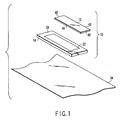
- a flip chip bonding configuration for a semiconductor package 10 that includes a semiconductor die 12 that is mechanically and electrically connected to a supporting substrate 14.
- Metallic bumps 16 on the bottom surface 18 of the die 12 overlap with metallic pads 20 correspondingly positioned in a die bonding region 22 located on the top surface 24 of the substrate 14.
- the metallic bumps 16 are connected to the underlying pads 20 by solder 26, thus providing direct electrical coupling between the die 12 and substrate 14.
- the direct electrical interconnection between the die 12 and substrate 14 provided by flip chip bonding configuration 10 advantageously eliminates the need for bond wires and results in low resistance and inductance values.
- flip chip bonding configurations provide for better signal integrity and power distribution to and from the die 12 than in other bonding technologies such as wire bonding or tape automated bonding.
- the bottom surface 18 of the die 12 may include hundreds of metallic bumps 16 with each metallic bump providing an electrical interface to and from the die 12 for various electrical signals, core power, input/output (I/O) power, and ground. Electrical signals, core power, and ground are provided to the die's internal logic circuitry (not shown). Similarly, the I/O power and ground are provided to the die's I/O interface circuitry (not shown), i.e., input and output drivers.
- the metallic bumps 16, and therefore the corresponding pads 20 on the top surface 24 of the substrate 14, generally are arranged in concentric rectangular rings (not shown) and are spaced apart to prevent electrical shorting between adjacent metallic bumps/pads. However, the metallic bumps 16 and pads 20 may be configured in various patterns other than concentric rectangular rings.
- the substrate 14 may be a multi-layer printed circuit board, ceramic substrate or another semiconductor chip. Typically, pads 28 on the bottom surface 30 of the substrate 14 are bonded, e.g., via solder 32, to another printed circuit board referred to as a motherboard 34.
- the substrate 14 provides for a mechanical and electrical interface between the often densely-packed metallic bumps 16 on the bottom surface 18 of the die 12 to less-densely packed pads (not shown) on the motherboard 34.
- the pads 28 on the substrate's bottom surface 30 are placed so as to correspond to the pads (not shown) on the motherboard 34.
- the various layers of the substrate 14 are formed by the well known processes used to create integrated circuits and printed circuit boards.
- the individual layers may be comprised of conductive or semiconductor material.
- the conductive material is a metal, i.e., a copper-based material, which is plated onto semiconductor material layers and patterned by photolithographically removing deposited metal to form pads and traces.
- the substrate 14 may be referred to as organic if organic material is combined with the copper-based material so as to provide thermal expansion characteristics close to those of the motherboard 34 and to improve reliability in board assembly.
- vias electrically interconnect pads 20 or 28 on either the top surface 24 or bottom surface 30 of the substrate 14 or to vias (not shown) which are holes that facilitate the electrical interconnection of the various layers of the substrate 14.
- the vias may be formed, for example, by mechanical or laser drilling a via hole through a layer or layers of the substrate 14. Surrounding the via hole on each level may be a circular land (not shown) made of a conductive material. Typically, the via hole is filled with a conductive material so that via lands surrounding the via holes on various layers of the substrate are electrically interconnected.
- a via may extend through to the bottom surface 30 of the substrate 14 and connect to a pad 28.
- solder balls 32 are individually connected to each pad 28 for soldering the pads 28 on the bottom surface 30 of the substrate 14 to the corresponding pads (not shown) on the motherboard 34.
- the solder balls 32 connected to the pads 28 on the bottom surface 30 of the substrate 14 are collectively called a ball grid array 36.
- the substrate 14 including maintaining a low DC resistance and AC inductance for power and ground connections to and from the die 12, and maintaining wide spacing between traces (not shown), pads 20 and 28, and via lands (not shown) to minimize the possibility of crosstalk or electrical shorting.
- the distance between the pads 20 on the top surface 24 of the substrate 14 for core power distribution and the logic circuitry which actually consume the power should be as short as possible.
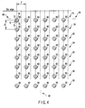
- FIG. 3 An exemplary C4 bonding technology pad arrangement 38 is shown in the top plan view of FIG. 3.
- the C4 bonding technology utilizes pads 40 arranged in an area array in the die bonding region 22 on the top surface 24 of the substrate 14 that are separated from one another by a pitch "p".
- the pads 40 are positioned at lattice points 41 (only numbered along one row and one column), where each lattice point 41 is located below the midpoint of each pad 40.
- the top two rows 42 and 44 of pads 40 from adjacent the die edge are rows of signal pads 46 that accommodate the transfer of various electrical signals to and from the die 12.
- the top two rows 42 and 44 of pads 40 closest to the die edge 48 include signal pads 46 because the majority of the logic circuitry within the die 12 is located proximate to the die edge 48 and signal traces (not shown) on the top surface 24 of the substrate 14 are typically routed outside of the die bonding region 22.
- the third and fourth rows 50 and 52, respectively, of pads 40 down from the die edge 48 include core power pads 54, for the transfer of power to the logic circuitry in the die 12, I/O power pads 56, for the transfer of power to the I/O interfaces in the die 12, and ground pads 58, for providing ground connections to the die.
- the fifth and sixth rows 60 and 62, respectively, of pads 40 down from the die edge 48 are again rows of signal pads 46.
- the seventh and eighth rows 64 and 66, respectively, of pads 40 are core power pads 54 and ground pads 58.
- power and ground pads 54 and 58, respectively are intermingled with the signal pads 46 so as to avoid problems that occur when large numbers of signal pads 46 result in the power and ground pads 54 and 58, respectively, being located further than three to four rows away from the die edge.
- the three dots 68 in the upper left hand corner, upper right hand corner, and the bottom of FIG. 3 indicate that the number and spacing between the pads 40 included in the pad arrangement 38 can vary along the top surface 24 of the substrate 14 in those directions.
- FIG. 3 indicates examples of the maximum distances between the die edge 48, where the logic circuitry is assumed to be located, and a core power pad 54 and an I/O power pad 56.
- a maximum distance between the die edge and a core power pad is approximately 3.354p (3.354 times p), where p is the pitch or distance between the midpoints of adjacent pads 40.
- a maximum distance between the die edge and an I/O power pad is approximately 4.272p (4.272 times p). If p is 0.25 millimeter, the distance between the die edge and the core power pad reaches approximately 0.8385 millimeter, and the distance between the die edge and the I/O power pad reaches approximately 1.068 millimeters. These distances may result in increased DC resistance and AC inductance values.
- FIG. 4 is a top plan view of underlying layers of vias 70 that connect to the pads 40 in FIG. 3.
- the vias 70 are used to rout electrical signals, core power, I/O power, and ground potential to the layers of the substrate 14 below the top surface 24.
- Each via 70 includes a via hole 72 indicated by the inside circle 73 with an accompanying ring-shaped via land 74 which surrounds the via hole 72 as indicated by the second concentric circle 75.
- the vias 70 in each underlying layer are located directly below the corresponding pads 40 at the lattice points 41 on the top surface 24 of the substrate 14, and thus, utilize a pad-on-via structure.
- the top two rows 76 and 78 of vias 70 adjacent the die edge 48 are rows of signal vias 80 that accommodate the transfer of various electrical signals.
- the third and fourth rows 82 and 84, respectively, of vias 70 down from the die edge 48 include core power vias 86, I/O power vias 88, and ground vias 90.
- the fifth and sixth rows 92 and 94, respectively, of vias 70 down from the die edge 48 are again rows of signal vias 80.
- the seventh and eighth rows 96 and 98, respectively, of vias 70 are core power vias 86 and ground vias 90.
- the three dots 68 in the upper left hand corner, upper right hand corner, and the bottom of FIG. 4 indicate that the number and spacing between the vias 70 included in the arrangement of vias 70 can vary along each layer in those directions.
- FIG. 5 is a top plan view of another C4 bonding configuration pad arrangement 100, based upon the pad arrangement 38 of FIG. 3, in which additional core power pads 54 and additional ground pads 58 are alternatingly placed in columns of core power pads 102 and columns of ground pads 104 at the interstitial points 106 (only numbered along one row and one column), where each interstitial point 106 is the mid point between four adjacent lattice points 41.
- FIG. 5 includes signal pads 46, core power pads 54, I/O power pads 56, and ground pads 58.
- the three dots 68 in the upper left hand corner, upper right hand corner, and the bottom of FIG. 5 indicate that the number and spacing between the pads 40 included in the pad arrangement 100 can vary along the top surface 24 of the substrate 14 in those directions.
- a maximum distance between a core power pad 54 and the die's logic circuitry, presumably located proximate to the die edge 48, is only approximately 1.803p (1.803 times p). Therefore, if p equals 0.25 millimeter, the distance between the core power pad and the logic circuitry will be approximately 0.4508 millimeter.
- the pad arrangement 100 of FIG. 5 offers improved power distribution performance over the pad arrangement 38 of FIG. 3.
- the C4 bonding configuration of FIG. 5 utilizes a pad-on-via structure as shown in the top plan view of underlying layers provided by FIG. 6.
- signal vias 80, core power vias 86, I/O power vias 88, and ground vias 90, respectively, are used to rout electrical signals, core power, I/O power, and ground potential to the layers of the substrate 14 below the top surface 24.
- the three dots 68 in the upper left hand corner, upper right hand corner, and the bottom of FIG. 6 indicate that the number a spacing between the vias included in the via arrangement can vary along each layer in those directions.
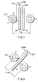
- FIG. 7 is a magnified top plan view of two signal traces 108 routed between two adjacent vias 70 for the C4 bonding configuration of FIGS. 3 and 4. As shown in FIG.
- the two traces 108 having a 28 micrometer trace width can be routed between the vias 70 leaving a 28 micrometer space between adjacent metal.
- FIG. 8 is a magnified top plan view of a signal trace 110 routed between two adjacent vias 70 for the C4 bonding technology configuration of FIGS. 5 and 6.
- only one trace 110 can be routed between the vias 70.
- a finer design spacing value of approximately 22 micrometers, instead of 28 micrometers, is required in FIG. 8. Therefore, if the C4 bonding configuration of FIGS. 5, 6, and 8 is to be used, more layers and a finer design spacing rule is required, both of which increase the overall cost for the substrate 14.
- a substrate has lattice points and interstitial points.
- the substrate includes a surface, a plurality of pads located on the surface at the lattice points and the interstitial points, and a plurality of vias formed in the substrate to be located at the lattice points and not located at at least one of the interstitial points.
- a semiconductor package in another aspect of the present invention, includes semiconductor die that has a die edge and a substrate connected to the semiconductor die that has lattice points and interstitial points.
- the substrate includes a surface, a plurality of pads located on the surface at the lattice points and the interstitial points, and a plurality of vias formed in the substrate to be located at the lattice points and not located at at least one of the interstitial points.
- a method for configuring vias in a substrate that has lattice points and interstitial points and for configuring pads on the surface of the substrate.
- the method includes locating pads on the surface of the substrate at interstitial points, and locating vias in the substrate only at lattice points.
- FIG. 9 is a top plan view of a top surface 24 of a substrate 14 in a die bonding region 22 and FIG. 10 is a corresponding underlying via layer of one exemplary embodiment of the present invention.
- FIG. 9 shows vertical columns 114 of pads 116 located at lattice points 118 (only numbered along one row and one column). The pads 116 located at the lattice points are electrically connected to vias 120 also located at lattice points 118 (only numbered along one row and one column) that pass through lower layers of the substrate 14 as shown in FIG. 10. These pads 116 that overly the vias 120 are referred to as "pad-on-vias" and are indicated by three concentric circles 122. Pads 140 without underlying vias 120 are located at the interstitial points 142 (only numbered along one row and one column) and are merely indicated by a single circle.
- the top two rows 124 and 126 of pad-on-vias 116 from the die edge 48 are rows of signal pads 46 that accommodate the transfer of various electrical signals to and from the die 12.
- the third and fourth rows 128 and 130, respectively, of pad-on-vias 116 down from the die edge 48 include core power pads 54, for the transfer of power to the logic circuitry in the die 12, I/O power pads 56, for the transfer of power to the I/O interfaces in the die 12, and ground pads 58, for providing ground connections to the die 12.
- the fifth and sixth rows 132 and 134, respectively, of pad-on-vias 116 down from the die edge 48 are again rows of signal pads 46.
- the seventh and eighth rows 136 and 138, respectively, of pad-on-vias 116 are core power pads 54 and ground pads 58.
- the pad arrangement 112 of FIG. 9 also includes vertical columns 139 of pads 140 without underlying vias 120 which are located at the interstitial points 142 (only numbered along one row and one column) and may be core power pads 54 or ground pads 58. Some of the pads 140 without underlying vias 120 are electrically interconnected by wide traces 144 as shown in FIG. 9. Also, some of the pads 140 without underlying vias 120 are electrically interconnected to the pad-on-vias 116 by means of either wide traces 146 or triangular-shaped metallic layers 148. This arrangement, allows for core power and ground to pass through the vias 120 to the underlying layers of the substrate 14.
- the three dots 68 in the upper left hand corner, upper right hand corner, and the bottom of FIG. 9 indicate that the number and spacing between the pads 116 included in the pad arrangement 112 can vary along the top surface 24 of the substrate 14 in those directions.
- each via hole 72 is indicated by the inside circle 73 with an accompanying ring-shaped via land 74 which surrounds the via hole 72 as indicated by the second concentric circle 75.
- the top two rows 150 and 152 of vias from the die edge 48 are rows of signal vias 80 that accommodate the transfer of various electrical signals.
- the third and fourth rows 154 and 156, respectively, of vias down from the die edge include core power vias 86, I/O power vias 88, and ground vias 90.
- the fifth and sixth rows 158 and 160, respectively, of vias 120 down from the die edge are again rows of signal vias 80.
- the seventh and eighth rows 162 and 164, respectively, of vias 120 are core power vias 86 and ground vias 90.
- the three dots 68 in the upper left hand corner, upper right hand corner, and the bottom of FIG. 10 indicate that the number and spacing between the vias 120 included in the via arrangement 149 can vary along each layer in those directions.
- a die 12 is mechanically connected to the top surface 24 of the substrate 14, for example, by soldering metal bumps (not shown) on the bottom surface 18 of the die 12 to pads 20 located on the top surface 24 of the substrate 14 in the die bonding region 22.
- the bottom surface 30 of the substrate 14 may be mechanically connected to a motherboard 34, for example, by soldering pads 28 on the bottom surface 30 of the substrate 14 to pads (not shown) on the motherboard 34.
- the die 12, substrate 14, and motherboard 34 are electrically interconnected, electrical signals, core power, I/O power, and ground can be electrically coupled through the substrate 14, by means of the pads 20 and 28, respectively, on both the substrate's top surface 24 and bottom surface 30, and the substrate's vias 120, to and from the die's internal circuitry, i.e., logic circuitry and I/O circuitry.
- the present invention advantageously offers a reduction in the distance between core power, I/O power, and ground pads 54, 56, and 58, respectively, and the logic circuitry located near the die edge 48.
- Embodiments of the present invention also maintain the via spacing of FIGS. 4 and 7, thus, allowing for at least two traces 108 to be routed between adjacent via lands 74 and eliminating the need for additional layers and narrower design spacing, both of which increase the overall cost of the substrate 14.
- the present invention provides wide traces 144 for core power and ground distribution which reduce DC resistance and AC inductance.
- the present invention provides improved performance over the C4 bonding pad and via configurations of FIGS. 3-8. Therefore, the present invention provides improved power distribution while maintaining conventional design spacing conventions.
Landscapes
- Wire Bonding (AREA)
- Internal Circuitry In Semiconductor Integrated Circuit Devices (AREA)
- Semiconductor Integrated Circuits (AREA)
Applications Claiming Priority (2)
| Application Number | Priority Date | Filing Date | Title |
|---|---|---|---|
| US10/141,685 US6768206B2 (en) | 2002-05-07 | 2002-05-07 | Organic substrate for flip chip bonding |
| US141685 | 2002-05-07 |
Publications (3)
| Publication Number | Publication Date |
|---|---|
| EP1361612A2 true EP1361612A2 (de) | 2003-11-12 |
| EP1361612A3 EP1361612A3 (de) | 2006-05-17 |
| EP1361612B1 EP1361612B1 (de) | 2008-08-20 |
Family
ID=29249820
Family Applications (1)
| Application Number | Title | Priority Date | Filing Date |
|---|---|---|---|
| EP03002079A Expired - Lifetime EP1361612B1 (de) | 2002-05-07 | 2003-01-30 | Organisches Flipchipbond-Substrat |
Country Status (4)
| Country | Link |
|---|---|
| US (1) | US6768206B2 (de) |
| EP (1) | EP1361612B1 (de) |
| JP (1) | JP3730625B2 (de) |
| DE (1) | DE60323003D1 (de) |
Cited By (2)
| Publication number | Priority date | Publication date | Assignee | Title |
|---|---|---|---|---|
| EP1471574A3 (de) * | 2003-04-24 | 2006-07-12 | Shinko Electric Industries Co., Ltd. | Verdrahtungssubstrat und Elektronikbauteil-Verpackungsstruktur |
| EP1753275A3 (de) * | 2005-08-10 | 2009-01-21 | Alcatel Lucent | Benutzung von der Reihen/Kolonnen von Mikro- vias in einem BGA-Verbindungsgitter für einen optimierten Leiterbahnenverlauf |
Families Citing this family (13)
| Publication number | Priority date | Publication date | Assignee | Title |
|---|---|---|---|---|
| US7105926B2 (en) * | 2003-11-24 | 2006-09-12 | Lsi Logic Corporation | Routing scheme for differential pairs in flip chip substrates |
| US7057284B2 (en) * | 2004-08-12 | 2006-06-06 | Texas Instruments Incorporated | Fine pitch low-cost flip chip substrate |
| US7081672B1 (en) * | 2005-03-07 | 2006-07-25 | Lsi Logic Corporation | Substrate via layout to improve bias humidity testing reliability |
| US7671450B2 (en) * | 2007-12-17 | 2010-03-02 | Agere Systems Inc. | Integrated circuit package for high-speed signals |
| US8186051B2 (en) * | 2008-03-28 | 2012-05-29 | Intel Corporation | Method for fabricating package substrate and die spacer layers having a ceramic backbone |
| US8552563B2 (en) | 2009-04-07 | 2013-10-08 | Taiwan Semiconductor Manufacturing Company, Ltd. | Three-dimensional semiconductor architecture |
| US8561004B2 (en) * | 2010-02-04 | 2013-10-15 | Advanced Micro Devices, Inc. | Ring power gating with distributed currents using non-linear contact placements |
| US8338948B2 (en) | 2010-06-30 | 2012-12-25 | International Business Machines Corporation | Ball grid array with improved single-ended and differential signal performance |
| EP2503594A1 (de) * | 2011-03-21 | 2012-09-26 | Dialog Semiconductor GmbH | Ball-/Padlayout einer integrierten Schaltungspackung mit optimiertem Signalrouting |
| EP2808890A4 (de) * | 2012-01-27 | 2015-08-19 | Panasonic Corp | Mehrschichtige leiterplatte |
| US9955605B2 (en) * | 2016-03-30 | 2018-04-24 | Intel Corporation | Hardware interface with space-efficient cell pattern |
| MY201172A (en) * | 2018-09-19 | 2024-02-08 | Intel Corp | Stacked through-silicon vias for multi-device packages |
| KR102254166B1 (ko) * | 2019-12-27 | 2021-05-20 | 주식회사 텔레칩스 | 볼 그리드 어레이 인쇄회로기판 |
Family Cites Families (24)
| Publication number | Priority date | Publication date | Assignee | Title |
|---|---|---|---|---|
| US5917229A (en) * | 1994-02-08 | 1999-06-29 | Prolinx Labs Corporation | Programmable/reprogrammable printed circuit board using fuse and/or antifuse as interconnect |
| JPH07245343A (ja) | 1994-03-03 | 1995-09-19 | Toshiba Corp | 半導体装置及びその製造方法 |
| JP3412942B2 (ja) * | 1995-01-11 | 2003-06-03 | 株式会社東芝 | 半導体装置 |
| KR970053805A (ko) | 1995-12-04 | 1997-07-31 | 김광호 | 반도체 메모리 장치의 파워라인 배치방법 |
| JPH09199587A (ja) | 1996-01-12 | 1997-07-31 | Nec Corp | 半導体装置 |
| US5763947A (en) * | 1996-01-31 | 1998-06-09 | International Business Machines Corporation | Integrated circuit chip package having configurable contacts and a removable connector |
| US5889326A (en) | 1996-02-27 | 1999-03-30 | Nec Corporation | Structure for bonding semiconductor device to substrate |
| JP3504421B2 (ja) | 1996-03-12 | 2004-03-08 | 株式会社ルネサステクノロジ | 半導体装置 |
| US5686764A (en) | 1996-03-20 | 1997-11-11 | Lsi Logic Corporation | Flip chip package with reduced number of package layers |
| US6160705A (en) * | 1997-05-09 | 2000-12-12 | Texas Instruments Incorporated | Ball grid array package and method using enhanced power and ground distribution circuitry |
| US5959348A (en) | 1997-08-18 | 1999-09-28 | International Business Machines Corporation | Construction of PBGA substrate for flip chip packing |
| US6031258A (en) | 1998-03-06 | 2000-02-29 | S3 Incorporated | High DC current stagger power/ground pad |
| US6323118B1 (en) | 1998-07-13 | 2001-11-27 | Taiwan Semiconductor For Manufacturing Company | Borderless dual damascene contact |
| US6084779A (en) | 1998-10-02 | 2000-07-04 | Sigrity, Inc. | Ground and power patches on printed circuit board signal planes in the areas of integrated circuit chips |
| US6166441A (en) | 1998-11-12 | 2000-12-26 | Intel Corporation | Method of forming a via overlap |
| DE19908428C2 (de) | 1999-02-26 | 2000-12-07 | Siemens Ag | Halbleiterspeicheranordnung mit Bitleitungs-Twist |
| US6140710A (en) * | 1999-05-05 | 2000-10-31 | Lucent Technologies Inc. | Power and ground and signal layout for higher density integrated circuit connections with flip-chip bonding |
| US6177732B1 (en) | 1999-05-27 | 2001-01-23 | Intel Corporation | Multi-layer organic land grid array to minimize via inductance |
| US6037677A (en) * | 1999-05-28 | 2000-03-14 | International Business Machines Corporation | Dual-pitch perimeter flip-chip footprint for high integration asics |
| JP2000349191A (ja) * | 1999-06-04 | 2000-12-15 | Toshiba Corp | 半導体装置および配線回路装置 |
| US6207476B1 (en) * | 1999-06-10 | 2001-03-27 | Vlsi Technology, Inc. | Methods of packaging an integrated circuit and methods of forming an integrated circuit package |
| US6150729A (en) * | 1999-07-01 | 2000-11-21 | Lsi Logic Corporation | Routing density enhancement for semiconductor BGA packages and printed wiring boards |
| US6340631B1 (en) | 2000-05-31 | 2002-01-22 | Taiwan Semiconductor Manufacturing Company, Ltd | Method for laying out wide metal lines with embedded contacts/vias |
| US6542377B1 (en) * | 2000-06-28 | 2003-04-01 | Dell Products L.P. | Printed circuit assembly having conductive pad array with in-line via placement |
-
2002
- 2002-05-07 US US10/141,685 patent/US6768206B2/en not_active Expired - Lifetime
-
2003
- 2003-01-17 JP JP2003009853A patent/JP3730625B2/ja not_active Expired - Fee Related
- 2003-01-30 EP EP03002079A patent/EP1361612B1/de not_active Expired - Lifetime
- 2003-01-30 DE DE60323003T patent/DE60323003D1/de not_active Expired - Lifetime
Cited By (4)
| Publication number | Priority date | Publication date | Assignee | Title |
|---|---|---|---|---|
| EP1471574A3 (de) * | 2003-04-24 | 2006-07-12 | Shinko Electric Industries Co., Ltd. | Verdrahtungssubstrat und Elektronikbauteil-Verpackungsstruktur |
| US7183647B2 (en) | 2003-04-24 | 2007-02-27 | Shinko Electric Industries, Co., Ltd. | Wiring substrate and electronic parts packaging structure |
| US7557450B2 (en) | 2003-04-24 | 2009-07-07 | Shinko Electric Industries Co., Ltd. | Wiring substrate and electronic parts packaging structure |
| EP1753275A3 (de) * | 2005-08-10 | 2009-01-21 | Alcatel Lucent | Benutzung von der Reihen/Kolonnen von Mikro- vias in einem BGA-Verbindungsgitter für einen optimierten Leiterbahnenverlauf |
Also Published As
| Publication number | Publication date |
|---|---|
| DE60323003D1 (de) | 2008-10-02 |
| EP1361612B1 (de) | 2008-08-20 |
| US6768206B2 (en) | 2004-07-27 |
| EP1361612A3 (de) | 2006-05-17 |
| JP2003332377A (ja) | 2003-11-21 |
| JP3730625B2 (ja) | 2006-01-05 |
| US20030209807A1 (en) | 2003-11-13 |
Similar Documents
| Publication | Publication Date | Title |
|---|---|---|
| US12191241B2 (en) | Fine pitch copper pillar package and method | |
| US7034391B2 (en) | Flip chip interconnection pad layout | |
| US10134663B2 (en) | Semiconductor device | |
| JP4592122B2 (ja) | パッケージ層の数を削減したフリップチップ・パッケージ | |
| US6768206B2 (en) | Organic substrate for flip chip bonding | |
| US20040238939A1 (en) | Multi-power ring chip scale package for system level integration | |
| EP0226433B1 (de) | Gedruckte Schaltungsplatte mit hoher Dichte | |
| US6815621B2 (en) | Chip scale package, printed circuit board, and method of designing a printed circuit board | |
| US8198724B1 (en) | Integrated circuit device having a multi-layer substrate and a method of enabling signals to be routed in a multi-layer substrate | |
| KR20020016867A (ko) | 라우팅층에 대한 신호 라인수를 최대화하기 위한 가변피치 콘택 어레이를 가진 집적 회로 다이 및/또는 패키지 | |
| US7180182B2 (en) | Semiconductor component | |
| CN100525578C (zh) | 用于提高电路板的定线密度的方法和这种电路板 | |
| US7105926B2 (en) | Routing scheme for differential pairs in flip chip substrates | |
| JP4494249B2 (ja) | 半導体装置 | |
| JP2001319997A (ja) | 半導体パッケージおよび半導体チップ | |
| US6828682B1 (en) | Substrate voltage connection | |
| JP4255447B2 (ja) | 半導体装置 | |
| JP2006319237A (ja) | 半導体装置 | |
| JP2000299401A (ja) | グリッドアレイパッケージ、プリント配線板及び電子機器 |
Legal Events
| Date | Code | Title | Description |
|---|---|---|---|
| PUAI | Public reference made under article 153(3) epc to a published international application that has entered the european phase |
Free format text: ORIGINAL CODE: 0009012 |
|
| 17P | Request for examination filed |
Effective date: 20030130 |
|
| AK | Designated contracting states |
Kind code of ref document: A2 Designated state(s): AT BE BG CH CY CZ DE DK EE ES FI FR GB GR HU IE IT LI LU MC NL PT SE SI SK TR |
|
| AX | Request for extension of the european patent |
Extension state: AL LT LV MK RO |
|
| PUAL | Search report despatched |
Free format text: ORIGINAL CODE: 0009013 |
|
| AK | Designated contracting states |
Kind code of ref document: A3 Designated state(s): AT BE BG CH CY CZ DE DK EE ES FI FR GB GR HU IE IT LI LU MC NL PT SE SI SK TR |
|
| AX | Request for extension of the european patent |
Extension state: AL LT LV MK RO |
|
| 17Q | First examination report despatched |
Effective date: 20060814 |
|
| AKX | Designation fees paid |
Designated state(s): DE FR GB |
|
| 17Q | First examination report despatched |
Effective date: 20060814 |
|
| GRAP | Despatch of communication of intention to grant a patent |
Free format text: ORIGINAL CODE: EPIDOSNIGR1 |
|
| GRAS | Grant fee paid |
Free format text: ORIGINAL CODE: EPIDOSNIGR3 |
|
| GRAA | (expected) grant |
Free format text: ORIGINAL CODE: 0009210 |
|
| AK | Designated contracting states |
Kind code of ref document: B1 Designated state(s): DE FR GB |
|
| REG | Reference to a national code |
Ref country code: GB Ref legal event code: FG4D |
|
| REF | Corresponds to: |
Ref document number: 60323003 Country of ref document: DE Date of ref document: 20081002 Kind code of ref document: P |
|
| PLBE | No opposition filed within time limit |
Free format text: ORIGINAL CODE: 0009261 |
|
| STAA | Information on the status of an ep patent application or granted ep patent |
Free format text: STATUS: NO OPPOSITION FILED WITHIN TIME LIMIT |
|
| 26N | No opposition filed |
Effective date: 20090525 |
|
| PGFP | Annual fee paid to national office [announced via postgrant information from national office to epo] |
Ref country code: FR Payment date: 20120202 Year of fee payment: 10 |
|
| PGFP | Annual fee paid to national office [announced via postgrant information from national office to epo] |
Ref country code: DE Payment date: 20120125 Year of fee payment: 10 |
|
| PGFP | Annual fee paid to national office [announced via postgrant information from national office to epo] |
Ref country code: GB Payment date: 20120125 Year of fee payment: 10 |
|
| GBPC | Gb: european patent ceased through non-payment of renewal fee |
Effective date: 20130130 |
|
| REG | Reference to a national code |
Ref country code: FR Ref legal event code: ST Effective date: 20130930 |
|
| PG25 | Lapsed in a contracting state [announced via postgrant information from national office to epo] |
Ref country code: DE Free format text: LAPSE BECAUSE OF NON-PAYMENT OF DUE FEES Effective date: 20130801 |
|
| REG | Reference to a national code |
Ref country code: DE Ref legal event code: R119 Ref document number: 60323003 Country of ref document: DE Effective date: 20130801 |
|
| PG25 | Lapsed in a contracting state [announced via postgrant information from national office to epo] |
Ref country code: GB Free format text: LAPSE BECAUSE OF NON-PAYMENT OF DUE FEES Effective date: 20130130 Ref country code: FR Free format text: LAPSE BECAUSE OF NON-PAYMENT OF DUE FEES Effective date: 20130131 |