EP1371993A2 - Capteur d'accélération et procédé de fabrication afférente - Google Patents
Capteur d'accélération et procédé de fabrication afférente Download PDFInfo
- Publication number
- EP1371993A2 EP1371993A2 EP20030010605 EP03010605A EP1371993A2 EP 1371993 A2 EP1371993 A2 EP 1371993A2 EP 20030010605 EP20030010605 EP 20030010605 EP 03010605 A EP03010605 A EP 03010605A EP 1371993 A2 EP1371993 A2 EP 1371993A2
- Authority
- EP
- European Patent Office
- Prior art keywords
- layer
- weight
- pedestal
- acceleration sensor
- section
- Prior art date
- Legal status (The legal status is an assumption and is not a legal conclusion. Google has not performed a legal analysis and makes no representation as to the accuracy of the status listed.)
- Granted
Links
Images









Classifications
-
- G—PHYSICS
- G01—MEASURING; TESTING
- G01P—MEASURING LINEAR OR ANGULAR SPEED, ACCELERATION, DECELERATION, OR SHOCK; INDICATING PRESENCE, ABSENCE, OR DIRECTION, OF MOVEMENT
- G01P15/00—Measuring acceleration; Measuring deceleration; Measuring shock, i.e. sudden change of acceleration
- G01P15/02—Measuring acceleration; Measuring deceleration; Measuring shock, i.e. sudden change of acceleration by making use of inertia forces using solid seismic masses
- G01P15/08—Measuring acceleration; Measuring deceleration; Measuring shock, i.e. sudden change of acceleration by making use of inertia forces using solid seismic masses with conversion into electric or magnetic values
- G01P15/125—Measuring acceleration; Measuring deceleration; Measuring shock, i.e. sudden change of acceleration by making use of inertia forces using solid seismic masses with conversion into electric or magnetic values by capacitive pick-up
-
- B—PERFORMING OPERATIONS; TRANSPORTING
- B81—MICROSTRUCTURAL TECHNOLOGY
- B81B—MICROSTRUCTURAL DEVICES OR SYSTEMS, e.g. MICROMECHANICAL DEVICES
- B81B3/00—Devices comprising flexible or deformable elements, e.g. comprising elastic tongues or membranes
- B81B3/0062—Devices moving in two or more dimensions, i.e. having special features which allow movement in more than one dimension
-
- G—PHYSICS
- G01—MEASURING; TESTING
- G01P—MEASURING LINEAR OR ANGULAR SPEED, ACCELERATION, DECELERATION, OR SHOCK; INDICATING PRESENCE, ABSENCE, OR DIRECTION, OF MOVEMENT
- G01P15/00—Measuring acceleration; Measuring deceleration; Measuring shock, i.e. sudden change of acceleration
- G01P15/02—Measuring acceleration; Measuring deceleration; Measuring shock, i.e. sudden change of acceleration by making use of inertia forces using solid seismic masses
- G01P15/08—Measuring acceleration; Measuring deceleration; Measuring shock, i.e. sudden change of acceleration by making use of inertia forces using solid seismic masses with conversion into electric or magnetic values
-
- G—PHYSICS
- G01—MEASURING; TESTING
- G01P—MEASURING LINEAR OR ANGULAR SPEED, ACCELERATION, DECELERATION, OR SHOCK; INDICATING PRESENCE, ABSENCE, OR DIRECTION, OF MOVEMENT
- G01P15/00—Measuring acceleration; Measuring deceleration; Measuring shock, i.e. sudden change of acceleration
- G01P15/02—Measuring acceleration; Measuring deceleration; Measuring shock, i.e. sudden change of acceleration by making use of inertia forces using solid seismic masses
- G01P15/08—Measuring acceleration; Measuring deceleration; Measuring shock, i.e. sudden change of acceleration by making use of inertia forces using solid seismic masses with conversion into electric or magnetic values
- G01P15/0802—Details
-
- G—PHYSICS
- G01—MEASURING; TESTING
- G01P—MEASURING LINEAR OR ANGULAR SPEED, ACCELERATION, DECELERATION, OR SHOCK; INDICATING PRESENCE, ABSENCE, OR DIRECTION, OF MOVEMENT
- G01P15/00—Measuring acceleration; Measuring deceleration; Measuring shock, i.e. sudden change of acceleration
- G01P15/02—Measuring acceleration; Measuring deceleration; Measuring shock, i.e. sudden change of acceleration by making use of inertia forces using solid seismic masses
- G01P15/08—Measuring acceleration; Measuring deceleration; Measuring shock, i.e. sudden change of acceleration by making use of inertia forces using solid seismic masses with conversion into electric or magnetic values
- G01P15/12—Measuring acceleration; Measuring deceleration; Measuring shock, i.e. sudden change of acceleration by making use of inertia forces using solid seismic masses with conversion into electric or magnetic values by alteration of electrical resistance
- G01P15/123—Measuring acceleration; Measuring deceleration; Measuring shock, i.e. sudden change of acceleration by making use of inertia forces using solid seismic masses with conversion into electric or magnetic values by alteration of electrical resistance by piezo-resistive elements, e.g. semiconductor strain gauges
-
- B—PERFORMING OPERATIONS; TRANSPORTING
- B81—MICROSTRUCTURAL TECHNOLOGY
- B81B—MICROSTRUCTURAL DEVICES OR SYSTEMS, e.g. MICROMECHANICAL DEVICES
- B81B2201/00—Specific applications of microelectromechanical systems
- B81B2201/02—Sensors
- B81B2201/0228—Inertial sensors
- B81B2201/0235—Accelerometers
-
- B—PERFORMING OPERATIONS; TRANSPORTING
- B81—MICROSTRUCTURAL TECHNOLOGY
- B81B—MICROSTRUCTURAL DEVICES OR SYSTEMS, e.g. MICROMECHANICAL DEVICES
- B81B2201/00—Specific applications of microelectromechanical systems
- B81B2201/02—Sensors
- B81B2201/0228—Inertial sensors
- B81B2201/0242—Gyroscopes
-
- B—PERFORMING OPERATIONS; TRANSPORTING
- B81—MICROSTRUCTURAL TECHNOLOGY
- B81B—MICROSTRUCTURAL DEVICES OR SYSTEMS, e.g. MICROMECHANICAL DEVICES
- B81B2203/00—Basic microelectromechanical structures
- B81B2203/05—Type of movement
- B81B2203/053—Translation according to an axis perpendicular to the substrate
-
- B—PERFORMING OPERATIONS; TRANSPORTING
- B81—MICROSTRUCTURAL TECHNOLOGY
- B81B—MICROSTRUCTURAL DEVICES OR SYSTEMS, e.g. MICROMECHANICAL DEVICES
- B81B2203/00—Basic microelectromechanical structures
- B81B2203/05—Type of movement
- B81B2203/055—Translation in a plane parallel to the substrate, i.e. enabling movement along any direction in the plane
-
- B—PERFORMING OPERATIONS; TRANSPORTING
- B81—MICROSTRUCTURAL TECHNOLOGY
- B81B—MICROSTRUCTURAL DEVICES OR SYSTEMS, e.g. MICROMECHANICAL DEVICES
- B81B2203/00—Basic microelectromechanical structures
- B81B2203/05—Type of movement
- B81B2203/056—Rotation in a plane parallel to the substrate
-
- B—PERFORMING OPERATIONS; TRANSPORTING
- B81—MICROSTRUCTURAL TECHNOLOGY
- B81B—MICROSTRUCTURAL DEVICES OR SYSTEMS, e.g. MICROMECHANICAL DEVICES
- B81B2203/00—Basic microelectromechanical structures
- B81B2203/05—Type of movement
- B81B2203/058—Rotation out of a plane parallel to the substrate
-
- G—PHYSICS
- G01—MEASURING; TESTING
- G01P—MEASURING LINEAR OR ANGULAR SPEED, ACCELERATION, DECELERATION, OR SHOCK; INDICATING PRESENCE, ABSENCE, OR DIRECTION, OF MOVEMENT
- G01P15/00—Measuring acceleration; Measuring deceleration; Measuring shock, i.e. sudden change of acceleration
- G01P15/02—Measuring acceleration; Measuring deceleration; Measuring shock, i.e. sudden change of acceleration by making use of inertia forces using solid seismic masses
- G01P15/08—Measuring acceleration; Measuring deceleration; Measuring shock, i.e. sudden change of acceleration by making use of inertia forces using solid seismic masses with conversion into electric or magnetic values
- G01P2015/0805—Measuring acceleration; Measuring deceleration; Measuring shock, i.e. sudden change of acceleration by making use of inertia forces using solid seismic masses with conversion into electric or magnetic values being provided with a particular type of spring-mass-system for defining the displacement of a seismic mass due to an external acceleration
- G01P2015/0822—Measuring acceleration; Measuring deceleration; Measuring shock, i.e. sudden change of acceleration by making use of inertia forces using solid seismic masses with conversion into electric or magnetic values being provided with a particular type of spring-mass-system for defining the displacement of a seismic mass due to an external acceleration for defining out-of-plane movement of the mass
- G01P2015/084—Measuring acceleration; Measuring deceleration; Measuring shock, i.e. sudden change of acceleration by making use of inertia forces using solid seismic masses with conversion into electric or magnetic values being provided with a particular type of spring-mass-system for defining the displacement of a seismic mass due to an external acceleration for defining out-of-plane movement of the mass the mass being suspended at more than one of its sides, e.g. membrane-type suspension, so as to permit multi-axis movement of the mass
-
- G—PHYSICS
- G01—MEASURING; TESTING
- G01P—MEASURING LINEAR OR ANGULAR SPEED, ACCELERATION, DECELERATION, OR SHOCK; INDICATING PRESENCE, ABSENCE, OR DIRECTION, OF MOVEMENT
- G01P15/00—Measuring acceleration; Measuring deceleration; Measuring shock, i.e. sudden change of acceleration
- G01P15/02—Measuring acceleration; Measuring deceleration; Measuring shock, i.e. sudden change of acceleration by making use of inertia forces using solid seismic masses
- G01P15/08—Measuring acceleration; Measuring deceleration; Measuring shock, i.e. sudden change of acceleration by making use of inertia forces using solid seismic masses with conversion into electric or magnetic values
- G01P2015/0805—Measuring acceleration; Measuring deceleration; Measuring shock, i.e. sudden change of acceleration by making use of inertia forces using solid seismic masses with conversion into electric or magnetic values being provided with a particular type of spring-mass-system for defining the displacement of a seismic mass due to an external acceleration
- G01P2015/0822—Measuring acceleration; Measuring deceleration; Measuring shock, i.e. sudden change of acceleration by making use of inertia forces using solid seismic masses with conversion into electric or magnetic values being provided with a particular type of spring-mass-system for defining the displacement of a seismic mass due to an external acceleration for defining out-of-plane movement of the mass
- G01P2015/084—Measuring acceleration; Measuring deceleration; Measuring shock, i.e. sudden change of acceleration by making use of inertia forces using solid seismic masses with conversion into electric or magnetic values being provided with a particular type of spring-mass-system for defining the displacement of a seismic mass due to an external acceleration for defining out-of-plane movement of the mass the mass being suspended at more than one of its sides, e.g. membrane-type suspension, so as to permit multi-axis movement of the mass
- G01P2015/0842—Measuring acceleration; Measuring deceleration; Measuring shock, i.e. sudden change of acceleration by making use of inertia forces using solid seismic masses with conversion into electric or magnetic values being provided with a particular type of spring-mass-system for defining the displacement of a seismic mass due to an external acceleration for defining out-of-plane movement of the mass the mass being suspended at more than one of its sides, e.g. membrane-type suspension, so as to permit multi-axis movement of the mass the mass being of clover leaf shape
-
- G—PHYSICS
- G01—MEASURING; TESTING
- G01P—MEASURING LINEAR OR ANGULAR SPEED, ACCELERATION, DECELERATION, OR SHOCK; INDICATING PRESENCE, ABSENCE, OR DIRECTION, OF MOVEMENT
- G01P15/00—Measuring acceleration; Measuring deceleration; Measuring shock, i.e. sudden change of acceleration
- G01P15/02—Measuring acceleration; Measuring deceleration; Measuring shock, i.e. sudden change of acceleration by making use of inertia forces using solid seismic masses
- G01P15/08—Measuring acceleration; Measuring deceleration; Measuring shock, i.e. sudden change of acceleration by making use of inertia forces using solid seismic masses with conversion into electric or magnetic values
- G01P2015/0862—Measuring acceleration; Measuring deceleration; Measuring shock, i.e. sudden change of acceleration by making use of inertia forces using solid seismic masses with conversion into electric or magnetic values being provided with particular means being integrated into a MEMS accelerometer structure for providing particular additional functionalities to those of a spring mass system
- G01P2015/0871—Measuring acceleration; Measuring deceleration; Measuring shock, i.e. sudden change of acceleration by making use of inertia forces using solid seismic masses with conversion into electric or magnetic values being provided with particular means being integrated into a MEMS accelerometer structure for providing particular additional functionalities to those of a spring mass system using stopper structures for limiting the travel of the seismic mass
Definitions
- the present invention relates to an acceleration sensor and a manufacturing method for the same, and more specifically, a mass production type acceleration sensor to be used for small-sized household electronic devices and a manufacturing method for the same.
- Household electronic devices with a microprocessor installed inside such as cell phones, digital cameras, electronic games, and PDAs have strongly spread, and recently, the demand for acceleration sensors to be installed in these electronic devices or input devices of electronic devices has also increased.
- acceleration components with an impact or a vibration applied to the device main body can be taken in the microprocessor as digital data, so that proper processing while grasping the physical environments around the electronic device becomes possible.
- correction for camera shake can be carried out by detecting the acceleration that has acted at the moment when the shutter button is pressed.
- an input device of an electronic game it also becomes possible to input a user' s operation instruction in the form of an acceleration.
- the acceleration sensor when used for detection of an gravity acceleration, the acceleration sensor can be used as a clinometer, and it becomes possible to recognize the azimuth of the entire electronic device (degree of inclination from the horizontal status), so that predetermined operation and input become possible based on a user's operation for inclining the entire electronic device.
- an acceleration sensor to be installed inside such a small-sized household electronic device is small-sized and suitable for mass production.
- Japanese Patent Publications No. 01-263576 and No. 03-202778 disclose structures of small-sized acceleration sensors suitable for mass production
- Japanese Patent Publication No. 04-249726 discloses a manufacturing method for mass production of such an acceleration sensor by using a silicon substrate.
- a general acceleration sensor a type has been generally used in which a weight is joined to a flexible substrate, and the substrate is bent in response to an acceleration applied to the weight, and the bend of this substrate is electrically detected.
- various detectors such as a piezo resistor element, a capacitor element, or a piezoelectric element have been used.
- a physical control structure such as a control substrate or a pedestal is provided for controlling vertical and horizontal displacements of the weight.
- a part of the weight comes into contact with the control substrate or the pedestal, and this suppresses displacements of the weight within a predetermined range of freedom. Therefore, the weight supporting portion can be prevented from being applied with an excessive stress and being broken.
- such a control structure has a predetermined shape and is disposed at a predetermined position in accordance with the shape and disposition of the weight. Therefore, in order to manufacture an acceleration sensor with a control structure, an etching step or machining step is additionally required, and this makes the manufacturing process complicated. Particularly, in order to secure uniform performance among lots to be manufactured as mass-produced items, it is required that the distance between the weight and the control structure is accurately set. Therefore, in the conventional acceleration sensors disclosed in the abovementioned publications, a great technical burden is imposed on the step for forming the control structure, and this also poses a problem in terms of cost reduction.
- An object of the invention is, therefore, to provide an acceleration sensor in which an accurate control structure for controlling displacements of the weight can be easily constructed.
- the basic structure of a transducer structure for acceleration detection to be used in an acceleration sensor relating to the invention Components forming the center of this transducer are a substrate layer and a weight. The weight is joined to a lower surface central portion of the substrate layer. When an acceleration is applied to the weight, due to this applied acceleration, the substrate layer partially displaces. In other words, this transducer structure functions to converts the acceleration into a displacement of the substrate layer.
- an acceleration sensor relating to the invention is obtained by adding a displacement detector which electrically detects a displacement to this transducer.
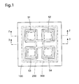
- Fig. 1 is a top view of a transducer structure relating to an embodiment of the invention.
- This transducer structure basically has a trilaminar structure composed of an upper layer 100 made from silicon, a middle layer 200 made from silicon oxide, and a lower layer 300 made from silicon.
- a material having such a trilaminar structure composed of silicon/silicon oxide/silicon is commercially available as an SOI (Silicon On Insulator) substrate, and the transducer structure shown herein can be manufactured by a manufacturing process using this SOI substrate.
- SOI Silicon On Insulator
- the upper layer 100, the middle layer 200, and the lower layer 300 are basically square plate members.
- slits S1 through S4 penetrating in the thickness direction are formed, and in Fig. 1, a part of the lower layer 300 is viewed through the slits S1 through S4.
- the structure of the middle layer 200 concealed under the upper layer 100 is shown by an alternate long and short dashed line, and the structure of the lower layer 300 is shown by a dashed line, so that this figure is complicated.
- Fig. 2 is a sectional side view along the cutting line 2-2 of the transducer structure of Fig. 1, and Fig.
- FIG. 3 is a sectional side view along the cutting line 3-3 of the transducer structure of Fig. 1.
- this transducer structure has a trilaminar structure composed of the upper layer 100, the middle layer 200, and the lower layer 300.
- components of the upper layer 100 are indicated by reference numerals between 100 and 199
- components of the middle layer 200 are indicated by reference numerals between 200 and 299
- components of the lower layer 300 are indicated by reference numerals between 300 and 399.
- Fig. 4 is a bottom view of this transducer structure, and in this bottom view, the structure of the middle layer 200 concealed by the lower layer 300 is shown by an alternate long and short dashed line, and the structure of the upper layer 100 is shown by a dashed line.
- Fig. 1 and the bottom view of Fig. 4 are convenient for confirmation of the relative positional relationship of the layers, however, they are complicated since all three layers are overlapped in a single drawing. Therefore, these figures are not necessarily appropriate to describe the fine structure of each layer. Therefore, by using plan views that independently show the respective layers, the structure of each layer is described in order while referring to the sectional side views of Fig. 2 and Fig. 3.
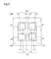
- FIG. 5 is a top view showing only the upper layer 100.
- the upper layer 100 is formed of a square plate member and has slits S1 through S4 penetrating in the thickness direction.
- the upper layer 100 is formed of a silicon substrate layer, and the slits S1 through S4 are formed by etching this silicon substrate layer as described later.
- the upper layer 100 can be divided into sections of a plurality of regions as seen in the figure.
- the dashed lines shown in Fig. 5 indicate boundaries of these regions for convenience. As a matter of course, these dashed lines do not indicate strict boundary positions of the respective regions, but are drawn in consideration of convenience in description.
- Fig. 6 is a horizontal sectional view along the cutting line 6-6 of the upper layer 100 of the sectional side view of Fig. 3, and clearly shows the shapes and dispositions of the slits S1 through S4 penetrating in the thickness direction.
- the slits S1 through S4 have angled annular narrow band shapes that are formed along outlines of almost squares. These shapes are not completely annular, and at a portion corresponding to one corner of the square, an aperture is formed, and respective sections are joined to each other via this aperture.
- the upper layer is structured as one substrate layer as a whole, and hereinafter, this upper layer 100 is referred to as a substrate layer 100 in some cases.
- the shapes of the four slits S1 through S4 are as completely same, however, the apertures of the respective slits are formed so as to face the center of the substrate layer 100 in a symmetric manner (symmetric horizontally and vertically in the plan view of Fig. 6).
- a fan-shaped structure is formed at the center of the substrate layer 100.
- the sections surrounded by the respective annular slits S1, S2, S3, and S4 are referred to as blade portions 111, 112, 113, and 114, respectively, and the square section at the center of the substrate layer 100 is referred to as a central portion 115.
- the fan-shaped structure is formed by these blade portions 111 through 114 and the central portion 115.
- this fan-shaped structure is referred to as a displacing section 110.
- connecting portions 121, 122, 123, and 124 herein (collectively referred to as a connecting section 120)
- the outer peripheral portion of the substrate layer 100 positioned at the outer side of the outer envelopes of the plurality of slit-s S1 through S4 is referred to as a fixed section 130.
- the substrate layer 100 is formed of a silicon substrate layer, and the connecting portions 121 through 124 having beam-like structures have physical properties that cause bending in response to action of an external force.
- the width and thickness (thickness of the substrate layer 100) of the connecting portions 121 through 124 are set so as to cause bending in response to action of an external force. Therefore, as described later, when an external force is applied to the displacing section 110, this external force is transmitted to the respective connecting portions 121 through 124 and causes them to bend. Consequently, the displacing section 110 is caused to displace with respect to the fixed section 130.
- the displacing section 110 at the center
- the fixed section 130 provided at the periphery of this displacing section 110
- the connecting section 120 for connecting the displacing section 110 to the fixed section 130 in a manner enabling the displacing section to displace.
- slits S1 through S4 are formed, however, it is not always necessary that these slits are square and these slits are four.
- a plurality of slits that have annular shapes partially including apertures are formed so that the apertures face the center of the substrate layer 100.
- a fan-shaped structure using the portions surrounded by the annular slits as blade portions can be regarded as a displacing section, the portions each of which are formed between a pair of slits adjacent to each other can be regarded as connecting portions, and the outer peripheral portion of the substrate layer 100 positioned at the outer side of the outer envelopes of the plurality of slits can be regarded as a fixed section.
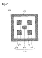
- Fig. 7 is a horizontal sectional view showing only the middle layer 200, and is equivalent to a horizontal sectional view along the cutting line 7-7 of the middle layer 200 of the sectional side view of Fig. 3.
- the middle layer 200 is formed by, as described later, etching a silicon oxide layer the layer surface of which is square.
- the middle layer 200 is composed of five weight joint layers 210 and a pedestal joint layer 230 that is disposed so as to surround these and has an angled annular shape. These joint layers have the same thickness.
- the weight joint layers 210 include four blade portion joint layers 211, 212, 213, and 214 and one central portion joint layer 215.
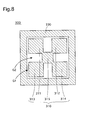
- Fig. 8 is a horizontal sectional view showing only the lower layer 300, and equivalent to a horizontal sectional view along the cutting line 8-8 of the lower layer 300 of the sectional side view of Fig. 3.
- the lower layer 300 is formed by, as described later, etching a silicon layer the layer surface of which is square. Grooves G1 and G2 shown in the figure are portions from which silicon has been removed by this etching.
- the lower layer 300 is composed of a fan-shaped weight 310 and a pedestal 330 that is disposed so as to surround the weight 310 and has an angled annular shape.
- the weight 310 consists of weight blade portions 311, 312, 313, and 314, and a weight central portion 315, and these correspond to the blade portions 111, 112, 113, and 114 and the central portion 115 that are included in the displacing section 110 shown in Fig. 5, and also correspond to the blade portion joint layers 211, 212, 213, and 214 and the central portion joint layer 215 of Fig. 7.
- the structures of the upper layer 100, the middle layer 200, and the lower layer 300 are individually described above, and a transducer structure relating to an embodiment described hereinafter is obtained by joining these three layers as shown in the top view of Fig. 1, the sectional side views of Fig. 2 and Fig. 3, and the bottom view of Fig. 4. Namely, to the lower surfaces of the blade portions 111 through 114 and the central portion 115 that are components of the upper layer 100 (substrate layer), the blade portion joint layers 211 through 214 and the central portion joint layer 215 that are components of the middle layer 200 are joined, and furthermore, to the lower surfaces of these, the weight blade portions 311 through 314 and the weight central portion 315 that are components of the lower layer 300 are joined.
- the weight joint layer 210 is composed of the respective blade portion joint layers 211 through 214 that join the displacing section 110 and the weight 310 at the positions of the blade portions of the fan shape, and the central joint layer 215 that joins the displacing section 110 and the weight 310 at the central position of the fan shape.
- the pedestal joint layer 230 composing the periphery of the middle layer 200 is joined, and to the lower surface of the pedestal joint layer 230, the pedestal 330 composing the periphery of the lower layer 300 is further joined.
- a control substrate 400 for example, glass substrate
- This control substrate 400 is for controlling downward displacements of the weight 310 as described later.
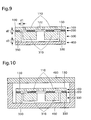
- the sectional side view of Fig. 10 shows an embodiment in which the bottom surface of the pedestal 330 is fixed to the bottom of a device casing 450, and a cover plate 460 is attached onto the top of the device casing 450 to closely seal it. In this case, the bottom of the device casing 450 serves as the control substrate.
- the weight 310 is attached to the lower surface of the substrate layer 100 (lower surface of the displacing section 110), and the fixed section 130 composing the periphery of the substrate layer 100 is supported and fixed by the pedestal 330.
- the displacing section 110 is supported in a manner enabling it to displace with respect to the fixed section 130 via the connecting section 120, so that the weight 310 is suspended in midair in the space surrounded by the pedestal 330.
- the acceleration acting on this detecting target also acts on the weight 310 as a reaction, and a force for displacing the weight 310 with respect to the pedestal 330 is generated.
- a force bends the connecting section 120, and the displacing section 110 relatively displaces with respect to the fixed section 130.
- the transducer structure described herein has a function for converting an applied acceleration into a displacement of the displacing section 110.
- the acceleration sensor relating to the invention detects the applied acceleration by detecting the displacement of the displacing section 110 thus caused by a displacement detector, and is realized by further adding the displacement detector to the transducer structure of Fig. 9 or Fig. 10.
- a detailed example of the displacement detector is described in Section 3. The operation of an acceleration sensor using this transducer structure in a case where an excessive acceleration is applied is described herein.
- the substrate layer 100 of the transducer structure relating to the embodiment shown herein is formed of a silicon substrate.
- slits S1 through S4 are formed in the substrate layer 100, and the connecting section 120 that is bent by a stress caused by an acceleration has an extremely delicate structure, and may be broken when being applied with an excessive acceleration. Therefore, a control structure which controls displacements of the weight 310 in a case where an excessive acceleration is applied is provided in the abovementioned transducer structure.
- a case where an excessive acceleration downward is applied to the weight 310 of the transducer structure of Fig. 9 is considered.
- a force acts to displace the weight 310 downward in the figure, however, the bottom surface of the weight 310 comes into contact with the upper surface of the control substrate 400, and this prevents the weight 310 from displacing over this upper surface.
- the bottom surface of the weight 310 is positioned at a predetermined distance d3 above the bottom surface of the pedestal 330 so that the predetermined distance d3 is secured between the bottom surface of the weight 310 and the upper surface of the control substrate 400 when the weight 310 is fixed above the control substrate 400.
- the weight 310 can freely displace downward within the range of the distance d3.
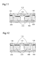
- an acceleration exceeding a predetermined tolerance is applied, as shown in the sectional side view of Fig. 11, the bottom surface of the weight 310 comes into contact with the upper surface of the control substrate 400 and its displacement is controlled.
- the predetermined distance d3 shown in Fig. 9 is a dimensional value that gives the weight 310 freedom in downward displacements, and this value is set within a safe range in which the substrate layer 100 is prevented from being broken upon consideration as to what degree of a downward displacement of the weight 310 causes the substrate layer 100 to break.
- Displacements of the weight 310 in the horizontal direction of the figure are controlled by the pedestal 330.
- the pedestal 330 is a structure surrounding all sides of the weight 310, so that all horizontal displacements of the weight 310 are controlled by the pedestal 330. Therefore, the predetermined distance d1 shown in Fig.
- 9 is a dimensional value that gives the weight 310 freedom in horizontal displacements, and the value is set within a safe range in which the substrate layer 100 is prevented from being broken upon consideration as to what degree of a horizontal displacement of the weight 310 causes the substrate layer 100 to break.
- displacements of the weight 310 in the upward direction in the figure are controlled by the control surface at the lower surface of the inner side of the fixed section 130.
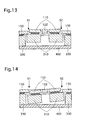
- the control surface at the lower surface of the inner side of the fixed section 130 For example, when the weight 310 shown in Fig. 9 is forcibly displaced upward in the figure, as shown in Fig. 13, the upper surface peripheral portion comes into contact with the lower surface (control surface) of the inside of the fixed section 130, whereby the weight is prevented from displacing further.
- Such displacement control is effective not only in the case where a force to displace the weight 310 vertically upward is applied but also in a case where rotation moment is applied to the weight 310. Namely, as shown in Fig. 14, even when a force to incline the weight 310 is applied, any portion of the upper surface periphery of the weight 310 comes into contact with the control surface of the lower surface of the inner side of the fixed section 130, whereby the weight is controlled so as not to further displace.
- Fig. 14 even when a force to incline the weight 310 is applied, any portion of the upper surface periphery of the weight 310 comes into contact with the control surface of the lower surface of the inner side of the fixed section 130, whereby the weight is controlled so as not to further displace.
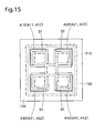
- the upper surface peripheral portion A12 of the weight 310 (the left end of the upper surface of the weight blade portion 311 in Fig. 2) is positioned immediately under the control surface A11 formed at the lower surface of the fixed section 130 so as to face the control surface.
- the right end of the weight blade portion 312 shown as a component of the lower layer 300 deviates rightward from the right end of the blade portion 112 shown as a component of the upper layer 100.
- the upper surface peripheral portion A22 of the weight 310 (the right end of the upper surface of the weight blade portion 312 in Fig. 2) is positioned immediately under the control surface A21 formed at the lower surface of the fixed section 130 so as to face the control surface.
- portions at the lower surface side of the fixed section 130 corresponding to the control regions A10, A20, A30, and A40 are referred to as the control surfaces A11, A21, A31, and A41
- portions at the upper surface side of the weight 310 corresponding to the control regions A10, A20, A30, and A40 are referred to as the upper surface peripheral portions A12, A22, A32, and A42, respectively.
- the control surfaces A11, A21, A31, and A41 are surfaces formed at the lower surface of the inner side of the fixed section 130 (in other words, surfaces formed in the regions outside and close to the slits 31 through S4 of the lower surface of the substrate layer 100), and the upper surface peripheral portions A12, A22, A32, and A42 are surfaces formed at the peripheral portion of the upper surface of the weight 310. Furthermore, since the upper surface peripheral portions A12, A22, A32, and A42 are disposed at the positions opposite to the control surfaces A11, A21, A31, and A41, upward displacements of the upper peripheral portions A12, A22, A32, and A42 are controlled as mentioned above.
- the contour of the upper surface of the weight 310 having a fan shape is formed by expanding the contour of the displacing section 110 having a fan shape outward, whereby displacement control by the control surfaces becomes possible at every portion of the upper peripheral portion of the weight 310.
- the middle layer 200 is formed from a material different from that of the upper layer (substrate layer) and the lower layer 300, so that the middle layer serves as a spacer interposed between the substrate layer 100 and the weight 310.
- the trilaminar structure including this middle layer 200 interposed to serve as a spacer it becomes possible to set the degree of freedom of upward displacements of the weight 310 to a fixed value (thickness of the middle layer 200). Therefore, even in mass production by means of a comparatively simple manufacturing process, the degree of freedom of weight displacements is prevented from significantly changing among lots.
- the weight joint layer 210 In order to make it possible for the weight 310 to displace upward within a predetermined range of freedom, it is necessary to interpose the weight joint layer 210 into a range other than the upper surface peripheral portions (region other than the control regions A10, A20, A30, and A40 shown by hatching in Fig. 15) in the space between the weight 310 and the substrate layer 100.
- the weight joint layer 210 (blade portion joint layers 211 through 214 and the central portion joint layer 215: see Fig. 7) is interposed at the position shown by an alternate long and short dashed line.
- the thickness of this weight joint layer 210 is set to an appropriate value so that upward displacements of the weight 310 are controlled within the predetermined range and the substrate layer 100 is prevented from being broken even when an applied acceleration exceeds the predetermined tolerance.
- the invention is characterized in that the structure for controlling upward displacements is accurately positioned by interposing a weight joint layer 210 that serves as a spacer between the substrate layer 100 and the weight 310.
- a weight joint layer 210 that serves as a spacer between the substrate layer 100 and the weight 310.
- the invention is characterized by the unique construction of the transducer structure, and any type of displacement detector can be used as long as the acceleration sensor uses the transducer structure of the invention.
- any type of displacement detector can be used as long as the acceleration sensor uses the transducer structure of the invention.
- two preferable detailed examples of displacement detector to be applied to the transducer structure mentioned above are shown hereinafter.
- the displacement detector comprises piezo resistor elements disposed on the connecting portions and detecting circuits for detecting changes in electric resistance of the piezo resistor elements.
- twelve piezo resistor elements Rx1 through Rx4, Ry1 through Ry4, and Rz1 through Rz4 are formed on the connecting portions 121, 122, 123, and 124.
- the substrate layer 100 is formed as an n-type silicon layer, and a p-type impurity is dispersed herein, whereby the respective piezo resistor elements can be formed (the relationship between the n-type and p-type may be inverted).
- the piezo resistor element has characteristics to change its electric resistance when a stress is applied.
- the connecting portions 121, 122, 123 and 124 bend due to the stress. Therefore, by detecting the electric resistance value of each of the piezo resistor elements, stresses applied to the connecting portions 121, 122, 123, and 124 can be recognized, the displacing status of the displacing section 110, and the direction and degree of the acceleration applied to the weight can be determined.
- connecting portions 121 and 124 are formed at both left and right sides of the displacing section 110, and two piezo resistor elements Rx1 and Rx2 are disposed at the left side connecting portion 121, and two piezo resistor elements Rx3 and Rx4 are disposed at the right side connecting portion 124 so that a total of four piezo resistor elements Rx1 through Rx4 are roughly lined up.
- a bridge circuit using these four piezo resistor elements Rx1 through Rx4 can detect an acceleration component concerning the aligning direction of the piezo resistor elements Rx1 through Rx4 or an acceleration component concerning the direction perpendicular to the substrate layer 100.
- an origin O is set at the center of the substrate layer 100, and as illustrated, the rightward direction of the figure is defined as an X axis, the upward direction of the figure is defined as a Y axis, and the vertically upward direction from the page surface of the figure is defined as a Z axis.
- a bridge circuit using the four piezo resistor elements Rx1 through Rx4 aligned along the X axis can detect an X axial component of an acceleration acting on the weight
- a bridge circuit using four piezo resistor elements Ry1 through Ry4 aligned along the Y axis can detect a Y axial component of the acceleration acting on the weight
- a bridge circuit using four piezo resistor elements Rz1 through Rz4 aligned along the X axis can detect a Z axial component of the acceleration acting on the weight.
- Fig. 17 is circuit diagram showing detecting circuits for detecting these bridges.
- voltages detected by these voltmeters 64, 65, and 66 indicate the X, Y, and Z axial components of an acceleration, respectively.
- the detection values became higher in accuracy in the layout of piezo resistor elements shown in Fig. 18 (the positions of the resistor elements Rx3 and Rx4 and the positions of the resistor elements Rz3 and Rz4 are replaced with each other) than in the layout of Fig. 16.
- the displacement detector comprises an auxiliary substrate disposed at a predetermined distance above the substrate layer, displacing electrodes formed on the upper surface of the displacing section, fixed electrodes formed on the lower surface of the auxiliary substrate, and detecting circuits that are comprised of the displacing electrodes and fixed electrodes for detecting changes in capacitance of capacitor elements.
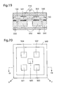
- an auxiliary substrate 500 is attached above the substrate layer 100 in the transducer structure shown in Fig. 9.
- the lower surface of the auxiliary substrate 500 is disposed at a predetermined distance from the upper surface of the substrate layer 100.
- five fixed electrodes 501, 502, 503, 504, and 505 are formed on the lower surface of this auxiliary substrate 500.
- the section of the auxiliary substrate 500 shown in the sectional side view of Fig. 19 is along the cutting line 19-19 of the auxiliary substrate 500 of Fig. 20.
- displacing electrodes are provided on the upper surface of the displacing section 110 so as to oppose these five fixed electrodes 501 through 505, and the fixed electrodes 501 through 505 and the displacing electrodes opposing these fixed electrodes form a total of five capacitor elements C1 through C5.
- at least regions of the upper surface of the displacing section 110 opposing the respective fixed electrodes 501 through 505 are formed as conductive regions, this displacing section 110 itself can be used as the displacing electrodes.
- the entire substrate layer 100 is formed of a conductive material (a silicon layer containing a high-density impurity dispersed) so that the entirety serves as one common electrode.
- the displacing status of the displacing section 110 can be recognized based on changes in capacitance of the five capacitor elements C1 through C5, and the direction and degree of an acceleration applied to the weight can be determined. Namely, the distance between the blade portions 111 through 114 and the central portion 115 that form the displacing section 110 and the auxiliary substrate 500 can be recognized based on the capacitance values of the capacitor elements C1 through C5, so that the degrees of respective directional components of the acceleration acting on the weight can be determined by means of operation based on these capacitance values.
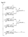
- Fig. 21 is a circuit diagram showing an example of detecting circuits which determine the respective directional components of an acceleration based on the principle mentioned above.
- the capacitor elements C1 through C5 in this circuit are constructed so that the conductive displacing section 110 is used as a common grounding electrode for one-side ends of the capacitor elements, and five fixed electrodes 501 through 505 are used as electrodes for other-side ends of the capacitor elements.
- the capacitance values of these capacitor elements are converted into voltage values V1 through V5 by C/V converters 71 through 75. Furthermore, a difference V1-V2 and a difference V3-V4 are determined by subtracters 76 and 77.
- the difference V1-V2 thus obtained at the output terminal Tx indicates an acceleration component in the X axial direction of Fig. 20
- the difference V3-V4 obtained at the output terminal Ty indicates an acceleration component in the Y axial direction of Fig. 20
- the voltage V5 obtained at the output terminal Tz indicates an acceleration component in the Z axial direction that is vertically upward from the page surface of Fig. 20.
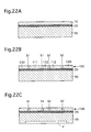
- FIG. 9 The sectional side views of Figs. 22 and Figs. 23 are equivalent to sectional views along the cutting line 2-2 of the transducer structure of Fig. 1.
- a material substrate formed by laminating a first layer 10, a second layer 20, and a third layer 30 in order from the top is prepared.
- the first layer 10 is a layer for composing the upper layer 100 (substrate layer), and in this embodiment, this is formed of a silicon layer.
- the second layer 20 is a layer for composing the middle layer 200 (joint layer), and in this embodiment, this is formed of a silicon oxide layer.
- the third layer 30 is a layer for composing the lower layer 300 (including the weight and pedestal), and in this embodiment, this is formed of a silicon layer.
- the material substrate having the trilaminar structure of silicon/silicon oxide/silicon is commercially available as an SOI substrate, and this commercially available SOI substrate is prepared from a practical standpoint.
- the first layer 10 and the second layer 20 are formed from materials with different etching properties
- the second layer 20 and the third layer 30 are formed from materials with different etching properties.
- the reason for this is that the second layer 20 must be used as an etching stopper layer when etching is applied to the first layer 10 from the upper side, and the second layer 20 must be used as an etching stopper layer when etching is applied to the third layer 30 from the lower side.
- the first layer 10 and the third layer 30 are formed from the same material (silicon), however, as a matter of course, the first layer 10, the second layer 20, and the third layer 30 can be formed from different materials.
- etching method which has erodibility for the first layer 10 and has no erodibility for the second layer 20
- predetermined regions of the first layer 10 are etched in the thickness direction until the upper surface of the second layer 20 is exposed to form slits in the first layer 10, whereby this first layer 10 is formed as a substrate layer 100 including a displacing section, a fixed section, and a connecting section.
- Slits formed herein are the slits S1 through S4 shown in Fig. 6. Therefore, in this etching step, a resist layer with a pattern corresponding to the hatching of Fig. 6 is formed on the upper surface of the first layer 10, and exposed portions that are not covered by this resist layer are eroded vertically downward.
- etching step the second layer 20 is not eroded, so that only the predetermined regions of the first layer 10 are removed.
- Fig. 22B shows the condition where the first layer 10 has been thus changed into the substrate layer 100.
- the blade portions 111 and 112 that are parts of the displacing section 110, the connecting portion 122 that is a part of the connecting section 120, and the fixed section 130 are shown. These parts are obtained by forming the slits S1 through S4 by means of etching (only S1 and S2 are shown in the figure).
- the lower layer portion of the region to be formed as the weight in the third layer 30 is removed by etching so that the thickness of the weight portion becomes smaller than that of the pedestal portion.
- a resist layer with a pattern corresponding to the region of the pedestal 330 of Fig. 8 is formed on the lower surface of the third layer 30, and exposed portions that are not covered by this resist layer are eroded vertically upward.
- Fig. 22C shows the condition where the third layer 30 has changed into the third layer 35 by this step.
- a void portion V is formed at the bottom of the third layer 35.
- the height of this void portion V regulates the dimension d3 in Fig. 9, and determines the degree of freedom of downward displacements of the weight 310.
- the height of the void portion V can be controlled to a desired set value by adjusting the etching period.
- etching method which has erodibility for the third layer 35 and has no erodibility for the second layer 20
- predetermined regions of the third layer 35 are etched in the thickness direction until the lower surface of the second layer 20 is exposed to separate the third layer 35 into the weight 310 and the pedestal 330.
- a resist layer with a pattern corresponding to the hatching of Fig. 8 is formed on the lower surface of the third layer 35, and exposed portions that are not covered by this resist layer, that is, portions equivalent to the grooves G1 and G2 are eroded vertically upward.
- erosion is not applied to the second layer 20, so that only the predetermined regions of the third layer 35 are removed.
- FIG. 23A shows the condition where the third layer 35 has been thus changed into the lower layer 300 that is formed of the weight 310 and the pedestal 330.
- the grooves G1 and G2 are formed, and at these portions, the lower surface of the second layer 20 is exposed.
- the groove G1 is formed more outwardly than the positions of the slits S1 and S2 formed in the substrate layer 100.
- This is in order to make the contour of the structure having a fan shape that forms the weight 310 in the lower layer 300 larger than that of the structure having a fan shape that forms the displacing section 110 in the substrate layer 100.
- the second layer 20 is etched in the. thickness direction and the layer surface direction from the exposed portions, and the remaining portions compose the weight joint layer 210 and the pedestal joint layer 230.
- this etching step it is not necessary to separately form a resist layer. Namely, as shown in Fig.
- the upper layer (substrate layer) 100 that is a remainder of the first layer 10 and the lower layer 300 that is a remainder of the third layer 30 serve as a resist layer for the second layer 20, and etching is applied to the exposed portions of the second layer 20, that is, regions for forming slits S1 through S4 and the grooves G1 and G2. Furthermore, herein, an etching method in which the second layer 20 is eroded not only in the thickness direction but also in the layer surface direction is used. As a result, as shown in Fig.
- portions around the vicinities of the slits S1 through S4 and the vicinities of the regions for forming the grooves G1 and G2 in the second layer 20 are removed by etching, whereby the weight joint layer 210 (only the blade portion joint layers 211 and 212 are shown in the figure) and the pedestal joint layer 230 are formed.
- the control substrate 400 (glass substrate in this embodiment) is joined to the bottom surface of the pedestal 330, whereby the structure of Fig. 23C is obtained.
- This is nothing less than the transducer structure shown in Fig. 9.
- the weight joint layer 210 and the pedestal joint layer 230 are formed by etching, the end faces of the joint layers composing the middle layer 200 are rounded, however, this does not influence joining of the substrate layer 100 and the lower layer 300.
- the etching method in the step for forming the substrate layer 100 by etching the first layer 10 vertically downward (Fig. 22B) and the step for forming the lower layer 300 by etching the third layer 35 vertically upward (Fig. 23A), it is required that the etching method satisfies the following two conditions.
- the first condition is that the etching method has erodibility with directivity in the thickness direction of each layer
- the second condition is that the etching method has no erodibility for a silicon oxide layer although it has erodibility for a silicon layer.
- the first condition is necessary to form slits and grooves with predetermined widths
- the second condition is necessary to use the second layer 20 made from silicon oxide as an etching stopper layer.
- ICP etching method an induced coupling plasma etching method
- This etching method is effective for forming deep grooves in the vertical direction, and is one of the etching methods called DRIE (Deep Reactive Ion Etching).
- DRIE Deep Reactive Ion Etching
- This method is characterized in that an etching step in which etching is carried out while eroding a material layer in the thickness direction and a deposition step in which a polymer wall is formed on the side surface of an etched hole are alternately repeated. The side surface of an etched hole is protected by a polymer wall that is successively formed, so that it becomes possible to advance erosion in only the thickness direction.
- an etching material having etching selectivity between silicon oxide and silicon is used.
- the inventor of this application carried out etching under the following conditions to satisfy these two conditions, and obtained successful results. That is, the abovementioned induced coupling plasma etching method was used and alternately repeated the etching step and the deposition step under the following detailed conditions.
- a material to be etched was put in a low-pressure chamber, and in the etching step, 100sccm of an SF 6 gas and 10sccm of an O 2 gas were supplied into the chamber, and in the deposition step, 100sccm of C 4 F 8 gas was supplied into the chamber.
- Etching was carried out at an etching rate of 3mm/min by repeating the etching step and the deposition step for 10 seconds each.
- This etching method can also be used in the step for forming the void portion V at the bottom of the third layer 30 (Fig. 22C).
- the manufacturing method of the invention is not limited to a method using the abovementioned etching method.
- the etching step of the second layer 20 (Fig. 23B) it is required that an etching method satisfying the following two conditions is used.
- the first condition is that the etching method causes erosion with directivity in the layer surface direction as well as the thickness direction
- the second condition is that the etching method has no erodibility for a silicon layer although it has erodibility for a silicon oxide layer.
- the first condition is necessary to prevent the joint layer from remaining at unnecessary portions and disturbing freedom in displacements of the weight
- the second condition is necessary to prevent erosion from reaching the substrate layer 100 and the lower layer 300 which are made from silicon and have already been etched into predetermined forms.
- etching was carried out.
- the same successful results were also obtained in dry-etching by an RIE method using a mixed gas of a CF 4 gas and an O 2 gas.
- the manufacturing method of the invention is not limited to a method using the abovementioned etching method.
- the abovementioned manufacturing method is advantageous in that the distance between the substrate layer 100 and the lower layer 300 does not change even if the conditions such as temperature, pressure, gas concentration, and period of etching slightly change.
- the distance between _these is equivalent to the dimension d2 shown in Fig. 9, and determines the degree of freedom of upward displacements of the weight 310, and this distance is always regulated by the thickness of the middle layer 200, and is not influenced by the etching conditions. Therefore, in mass production of acceleration sensors by the manufacturing method of the invention, accurate setting of dimensions becomes possible without unevenness among lots.
- control surfaces A11 A21, A31, and A41 of the fixed section 130 and the upper surface peripheral portions A12, A22, A32, and A42 of the weight 310 are opposed to each other in the control regions A10, A20, A30, and A40 that are shown by hatching in Fig. 15, whereby displacement control is made.
- the widths of the control regions A10, A20, A30, and A40 are extremely narrow, and therefore, if a dimensional error occurs between the positions of the slits S1 through S4 and the position of the weight 310, there is a possibility that these control regions are not correctly formed.
- the area of the illustrated control region A10 is reduced by the deviation of the slit S1 and on the other hand, the area of the illustrated control region A40 increases due to the deviation of the slit S4. Therefore, when the degree of deviation reaches a certain extent, the control region A10 completely disappears, and the displacement control function at the upper left portion of the figure is completely lost.
- each portion is formed by means of etching, so that the abovementioned deviation may occur unless the etching positions are satisfactorily accurate.
- a lot the displacement control function of which is incomplete due to etching failures must be excluded as a defective.
- a first modification example to be described herein is for solving this problem.
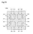
- the upper layer 100A shown in the horizontal sectional view of Fig. 24 is used in place of the upper layer 100 shown in the horizontal sectional view of Fig. 6.
- This upper layer 100A is characterized in that hoof-formed slits S11 through S14, S21 through S24, S31 through S34, and S41 through S44 are formed around the slits S1, S2, S3, and S4.
- These hoof-formed slits function as checking windows for a visual check of the contour position of the weight 310.
- Fig. 25 is a top view of the transducer structure using this upper layer 100A. As in Fig.
- the control regions A10, A20, A30 and A40 shown by hatching are for performing the displacement control function.
- the hoof-formed slits are formed in the structure shown in Fig. 25, so that the contour position of the weight 310 can be visually checked through the hoof-formed slits .
- the position of the left side contour portion of the weight blade portion 311 can be checked by viewing the insides of the illustrated hoof-formed slits S11 and S12.
- Fig. 26 is an enlarged top view around the hoof-formed slit S11 of Fig. 25.
- the weight blade portion 311 is positioned on the right and the groove G1 is positioned on the left.
- the boundary between these shows the left side contour position of the weight blade portion 311. Therefore, by viewing the inside of each hoof-formed slit dispersedly disposed at the upper layer 100A, the entire contour of the weight 310 can be recognized, and it can be judged whether or not the control regions A10, A20, A30, and A40 have been correctly formed.
- the same judgement can be made by enlarging it with optical means such as a microscope.
- optical means such as a microscope.
- the area of the control regions is slightly reduced, however, this hardly influences the displacement control function.
- the "upper surface peripheral portions" of the weight and the “control surfaces” formed at the lower surface of the inner side of the fixed section in the invention are not necessarily formed so as to completely surround the periphery of the weight, and are allowed to disperse at portions at which efficient control of displacements of the weight is possible.
- a second modification example to be described next is an example of a further reduction in area of the control regions.
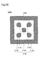
- an upper layer 100B shown in Fig. 27 is used in place of the upper layer 100 shown in Fig. 6, a middle layer 200B shown in Fig. 28 is used in place of the middle layer 200 shown in Fig. 7, and a lower layer 300B shown in Fig. 29 is used in place of the lower layer 300 shown in Fig. 8 (all of these figures are horizontal sectional views cut along surfaces parallel to the layer surfaces).
- slits SS1 through SS4 have been formed. These slits are not square but nearly octagonal. All of these slits are not perfectly annular octagonal, and have apertures at portions close to the center of the upper layer 100B. In other words, these slits SS1 through SS4 are shaped by chamfering the three corners of each of square-shaped slits S1 through S4 that are formed at the upper layer 100 of Fig. 6. In actuality, this chamfered corner serves as a control surface. On the other hand, the middle layer 200B shown in Fig.
- the lower layer 300B shown in Fig. 29 is composed of a weight 310B having a fan shape (including the weight blade portions 311B through 314B and weight central portion 315B) and a pedestal 330B surrounding this weight, and these are separated from each other by grooves GG1 and GG2.
- the weight blade portions 311B through 314B shown in Fig. 29 are square
- the blade portion joint layers 211B through 214B shown in Fig. 28 are shaped by chamfering the three corners of each square.
- each square of the weight blade portions 311B through 314B serve as upper peripheral portions, however, the blade portion joint layers 211B through 214B are shaped by omitting these regions of the upper surface peripheral portions, so that a predetermined distance d2 (thickness of the middle layer 200B is secured between the upper surface peripheral portions and control surfaces, and this makes it possible for the weight 310B to displace upward within the range of the degree of freedom corresponding to the distance d2.
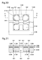
- Fig. 30 is a top view of a transducer structure formed by laminating the upper layer 100B, the middle layer 200B, and the lower layer 300B (a part of the lower layer 300B is shown by a dashed line, and the middle layer 200B is omitted in the figure).
- the lower half of the figure shows a condition where the upper layer 100B and the middle layer 200B are removed (that is, the upper surface of the lower layer 300B).
- the two-dimensional positional relationship between the slits SS1 through SS4 formed at the upper layer 100B and the weight 310 can be clearly recognized.
- the regions with hatching are the control regions, and the control regions at the lower surface of the upper layer 100B serve as “control surfaces”, and the control regions at the upper surface of the weight 310B serve as "upper surface peripheral portions".
- the control regions AA1, AA2, and AA3 are controlled by the control regions AA1, AA2, and AA3 at the three positions as illustrated. Displacements of the four weight blade portions 311B through 314B are controlled at three points, respectively.
- the upper surface peripheral portions opposing the control surfaces are not necessarily provided at the entire periphery of the upper surface of the weight 310, and it is sufficient that they are provided at a part of the periphery as the regions with hatching shown in Fig. 30.
- the connecting portion 120B is comparatively hard, it is possible to further reduce the number of control regions.
- three control regions AA1, AA2, and AA3 are provided at the periphery of the slit SS1, however, it is also possible to reduce these to only one control region AA2.
- Fig. 31 is a sectional side view showing a condition where the transducer structure of Fig. 30 is cut along the cutting line 31-31 of Fig. 30. As illustrated, a groove GG1 of the lower layer 300B is formed immediately under the slits SS1 and SS2 of the upper layer 100B, and as far as this sectional side view shows, no structure for controlling displacements of the weight 310B by the lower surface of the fixed section 130B is shown. However, in the structure shown in Fig.
- the acceleration sensor and the manufacturing method for the same of the invention easily achieve an accurate control structure for limiting displacements of the weight.
Landscapes
- Physics & Mathematics (AREA)
- General Physics & Mathematics (AREA)
- Engineering & Computer Science (AREA)
- Computer Hardware Design (AREA)
- Microelectronics & Electronic Packaging (AREA)
- Pressure Sensors (AREA)
Applications Claiming Priority (2)
| Application Number | Priority Date | Filing Date | Title |
|---|---|---|---|
| JP2002136596A JP4216525B2 (ja) | 2002-05-13 | 2002-05-13 | 加速度センサおよびその製造方法 |
| JP2002136596 | 2002-05-13 |
Publications (3)
| Publication Number | Publication Date |
|---|---|
| EP1371993A2 true EP1371993A2 (fr) | 2003-12-17 |
| EP1371993A3 EP1371993A3 (fr) | 2004-12-01 |
| EP1371993B1 EP1371993B1 (fr) | 2016-04-06 |
Family
ID=29397532
Family Applications (1)
| Application Number | Title | Priority Date | Filing Date |
|---|---|---|---|
| EP03010605.8A Expired - Lifetime EP1371993B1 (fr) | 2002-05-13 | 2003-05-12 | Capteur d'accélération et procédé de fabrication afférente |
Country Status (4)
| Country | Link |
|---|---|
| US (2) | US6772632B2 (fr) |
| EP (1) | EP1371993B1 (fr) |
| JP (1) | JP4216525B2 (fr) |
| CN (1) | CN100374865C (fr) |
Families Citing this family (84)
| Publication number | Priority date | Publication date | Assignee | Title |
|---|---|---|---|---|
| US6864677B1 (en) * | 1993-12-15 | 2005-03-08 | Kazuhiro Okada | Method of testing a sensor |
| US5421213A (en) * | 1990-10-12 | 1995-06-06 | Okada; Kazuhiro | Multi-dimensional force detector |
| US6314823B1 (en) * | 1991-09-20 | 2001-11-13 | Kazuhiro Okada | Force detector and acceleration detector and method of manufacturing the same |
| US6282956B1 (en) * | 1994-12-29 | 2001-09-04 | Kazuhiro Okada | Multi-axial angular velocity sensor |
| US6809529B2 (en) * | 2001-08-10 | 2004-10-26 | Wacoh Corporation | Force detector |
| JP4125931B2 (ja) * | 2002-08-26 | 2008-07-30 | 株式会社ワコー | 回転操作量の入力装置およびこれを利用した操作装置 |
| JP4907050B2 (ja) * | 2003-03-31 | 2012-03-28 | 株式会社ワコー | 力検出装置 |
| JP4387691B2 (ja) * | 2003-04-28 | 2009-12-16 | 株式会社ワコー | 力検出装置 |
| EP1491901A1 (fr) | 2003-06-25 | 2004-12-29 | Matsushita Electric Works, Ltd. | Capteur d'accélération sémiconducteur et méthode pour sa fabrication |
| JP2005049130A (ja) * | 2003-07-30 | 2005-02-24 | Oki Electric Ind Co Ltd | 加速度センサ及び加速度センサの製造方法 |
| JP4416460B2 (ja) * | 2003-09-16 | 2010-02-17 | トレックス・セミコンダクター株式会社 | 加速度センサー |
| JP4552002B2 (ja) * | 2003-10-23 | 2010-09-29 | 東亜ディーケーケー株式会社 | 気液分離膜およびその製造方法 |
| JP4578087B2 (ja) * | 2003-11-10 | 2010-11-10 | Okiセミコンダクタ株式会社 | 加速度センサ |
| US7397097B2 (en) * | 2003-11-25 | 2008-07-08 | Stmicroelectronics, Inc. | Integrated released beam layer structure fabricated in trenches and manufacturing method thereof |
| US7501835B2 (en) * | 2004-03-10 | 2009-03-10 | Kabushiki Kaisha Toyota Chuo Kenkyusho | Displacement sensor |
| JP2005283402A (ja) * | 2004-03-30 | 2005-10-13 | Fujitsu Media Device Kk | 慣性センサ |
| JP2005283393A (ja) * | 2004-03-30 | 2005-10-13 | Fujitsu Media Device Kk | 慣性センサ |
| JP4272115B2 (ja) * | 2004-06-03 | 2009-06-03 | Okiセミコンダクタ株式会社 | 加速度センサ及びその製造方法 |
| JP2006062002A (ja) * | 2004-08-25 | 2006-03-09 | Oki Electric Ind Co Ltd | 半導体装置の個片化方法 |
| US7353706B2 (en) * | 2004-12-28 | 2008-04-08 | Stmicroelectronics, Inc. | Weighted released-beam sensor |
| US7179674B2 (en) * | 2004-12-28 | 2007-02-20 | Stmicroelectronics, Inc. | Bi-directional released-beam sensor |
| JP2006242692A (ja) * | 2005-03-02 | 2006-09-14 | Oki Electric Ind Co Ltd | 加速度センサチップ |
| JP2006250581A (ja) * | 2005-03-08 | 2006-09-21 | Mitsumi Electric Co Ltd | 3軸加速度センサモジュールおよびその製造方法 |
| JP2006275896A (ja) * | 2005-03-30 | 2006-10-12 | Yokohama Rubber Co Ltd:The | 半導体加速度センサ |
| JP4815857B2 (ja) * | 2005-04-26 | 2011-11-16 | 大日本印刷株式会社 | 力学量検出センサの製造方法 |
| US7337671B2 (en) * | 2005-06-03 | 2008-03-04 | Georgia Tech Research Corp. | Capacitive microaccelerometers and fabrication methods |
| US7318349B2 (en) * | 2005-06-04 | 2008-01-15 | Vladimir Vaganov | Three-axis integrated MEMS accelerometer |
| US7578189B1 (en) | 2006-05-10 | 2009-08-25 | Qualtre, Inc. | Three-axis accelerometers |
| JP2007309654A (ja) * | 2006-05-16 | 2007-11-29 | Sony Corp | 加速度センサおよびその製造方法 |
| US20080041156A1 (en) * | 2006-07-05 | 2008-02-21 | Oki Electric Industry Co., Ltd. | Semiconductor acceleration sensor |
| JP5007083B2 (ja) * | 2006-08-08 | 2012-08-22 | 本田技研工業株式会社 | 力覚センサ用チップ |
| JP4858064B2 (ja) * | 2006-10-04 | 2012-01-18 | 大日本印刷株式会社 | 力学量検出センサおよびその製造方法 |
| EP2090866A4 (fr) * | 2006-11-20 | 2011-08-31 | Dainippon Printing Co Ltd | Détecteur de quantité dynamique, et procédé pour sa fabrication |
| JP2008190931A (ja) | 2007-02-02 | 2008-08-21 | Wacoh Corp | 加速度と角速度との双方を検出するセンサ |
| JP4858215B2 (ja) * | 2007-02-20 | 2012-01-18 | パナソニック株式会社 | 複合センサ |
| JP2008224254A (ja) * | 2007-03-08 | 2008-09-25 | Oki Electric Ind Co Ltd | センサ装置、センサ装置の製造方法 |
| JP2008249390A (ja) * | 2007-03-29 | 2008-10-16 | Oki Electric Ind Co Ltd | 半導体装置及びその製造方法 |
| JPWO2008143191A1 (ja) * | 2007-05-17 | 2010-08-05 | ローム株式会社 | Memsセンサおよびその製造方法 |
| JP2007279055A (ja) * | 2007-05-29 | 2007-10-25 | Oki Electric Ind Co Ltd | 加速度センサの製造方法 |
| JP2009020001A (ja) * | 2007-07-12 | 2009-01-29 | Oki Electric Ind Co Ltd | 加速度センサ |
| DE102007046017B4 (de) * | 2007-09-26 | 2021-07-01 | Robert Bosch Gmbh | Sensorelement |
| JP5186885B2 (ja) | 2007-11-07 | 2013-04-24 | 大日本印刷株式会社 | マスクパターンの補正方法およびそれを用いた加速度センサと角速度センサの製造方法 |
| US8136400B2 (en) * | 2007-11-15 | 2012-03-20 | Physical Logic Ag | Accelerometer |
| JP4687736B2 (ja) * | 2008-03-25 | 2011-05-25 | 株式会社村田製作所 | 外力検知装置の製造方法および外力検知装置 |
| JP5147491B2 (ja) * | 2008-03-28 | 2013-02-20 | ラピスセミコンダクタ株式会社 | 加速度センサ装置 |
| JP5253859B2 (ja) * | 2008-03-28 | 2013-07-31 | ラピスセミコンダクタ株式会社 | 加速度センサの構造及びその製造方法 |
| US7968353B2 (en) * | 2008-04-15 | 2011-06-28 | Global Solar Energy, Inc. | Apparatus and methods for manufacturing thin-film solar cells |
| JP5108617B2 (ja) | 2008-05-13 | 2012-12-26 | 大日本印刷株式会社 | 加速度センサ |
| JP2010085143A (ja) * | 2008-09-30 | 2010-04-15 | Torex Semiconductor Ltd | 加速度センサー |
| JP2010107242A (ja) * | 2008-10-28 | 2010-05-13 | Rohm Co Ltd | Memsセンサ |
| JP5293145B2 (ja) * | 2008-12-17 | 2013-09-18 | 大日本印刷株式会社 | 半導体装置 |
| US20100162823A1 (en) * | 2008-12-26 | 2010-07-01 | Yamaha Corporation | Mems sensor and mems sensor manufacture method |
| TWI391663B (zh) * | 2009-02-25 | 2013-04-01 | Nat Univ Tsing Hua | 加速度計 |
| TW201034932A (en) * | 2009-03-31 | 2010-10-01 | Domintech Co Ltd | Capacitor type three-axis accelerometer for microelectromechanical systems (MEMS) |
| JP5439068B2 (ja) * | 2009-07-08 | 2014-03-12 | 株式会社ワコー | 力検出装置 |
| JP5724342B2 (ja) * | 2009-12-10 | 2015-05-27 | 大日本印刷株式会社 | パターン配置方法並びにシリコンウェハ及び半導体デバイスの製造方法 |
| KR101119283B1 (ko) * | 2009-12-22 | 2012-06-05 | 삼성전기주식회사 | 관성 센서 및 그 제조 방법 |
| KR20120131788A (ko) * | 2011-05-26 | 2012-12-05 | 삼성전기주식회사 | 관성센서 및 그 제조방법 |
| CN102959403B (zh) | 2010-06-21 | 2015-11-25 | 大日本印刷株式会社 | 力学量传感器 |
| CN102408089A (zh) * | 2010-09-20 | 2012-04-11 | 利顺精密科技股份有限公司 | 可同时量测加速度及压力的微机电传感器 |
| KR101264549B1 (ko) | 2011-11-11 | 2013-05-14 | 삼성전기주식회사 | 관성센서의 제조방법 |
| KR101354757B1 (ko) * | 2011-11-18 | 2014-01-22 | 삼성전기주식회사 | 관성센서 |
| US8984942B2 (en) * | 2012-02-10 | 2015-03-24 | Hewlett-Packard Development Company, L.P. | Suspended masses in micro-mechanical devices |
| TWI586946B (zh) * | 2013-02-04 | 2017-06-11 | Fujikura Ltd | Sensing detectors |
| JP6339669B2 (ja) | 2013-07-08 | 2018-06-06 | モーション・エンジン・インコーポレーテッド | Memsデバイスおよび製造する方法 |
| US10273147B2 (en) | 2013-07-08 | 2019-04-30 | Motion Engine Inc. | MEMS components and method of wafer-level manufacturing thereof |
| WO2015013827A1 (fr) | 2013-08-02 | 2015-02-05 | Motion Engine Inc. | Capteur de mouvement à système microélectromécanique (mems) pour détection de vitesse angulaire de sous-résonance |
| JP5529328B1 (ja) | 2013-09-04 | 2014-06-25 | 株式会社トライフォース・マネジメント | 発電素子 |
| KR20150049056A (ko) * | 2013-10-29 | 2015-05-08 | 삼성전기주식회사 | 가속도 센서 |
| WO2015103688A1 (fr) | 2014-01-09 | 2015-07-16 | Motion Engine Inc. | Système mems intégré |
| US20170030788A1 (en) | 2014-04-10 | 2017-02-02 | Motion Engine Inc. | Mems pressure sensor |
| US11674803B2 (en) | 2014-06-02 | 2023-06-13 | Motion Engine, Inc. | Multi-mass MEMS motion sensor |
| US11287486B2 (en) | 2014-12-09 | 2022-03-29 | Motion Engine, Inc. | 3D MEMS magnetometer and associated methods |
| US10407299B2 (en) | 2015-01-15 | 2019-09-10 | Motion Engine Inc. | 3D MEMS device with hermetic cavity |
| US10416030B2 (en) | 2015-01-26 | 2019-09-17 | Wacoh-Tech Inc. | Force sensor |
| JP6002868B1 (ja) | 2015-04-07 | 2016-10-05 | 株式会社トライフォース・マネジメント | 力覚センサおよびこれに用いる構造体 |
| KR20160126211A (ko) | 2015-04-23 | 2016-11-02 | 삼성전기주식회사 | 관성 센서 |
| JP6527801B2 (ja) * | 2015-09-30 | 2019-06-05 | 日立オートモティブシステムズ株式会社 | 物理量センサ |
| JP5996078B1 (ja) | 2015-10-19 | 2016-09-21 | 株式会社トライフォース・マネジメント | 発電素子 |
| JP2017187447A (ja) * | 2016-04-08 | 2017-10-12 | アルプス電気株式会社 | センサ装置 |
| US11150092B2 (en) | 2017-01-17 | 2021-10-19 | Panasonic Intellectual Property Management Co., Ltd. | Sensor |
| CN107271724A (zh) * | 2017-05-18 | 2017-10-20 | 中北大学 | 单片集成的压阻式三轴加速度计及制备方法 |
| IT201700071798A1 (it) | 2017-06-27 | 2018-12-27 | St Microelectronics Srl | Sensore di forza multiassiale, metodo di fabbricazione del sensore di forza multiassiale, e metodo di funzionamento del sensore di forza multiassiale |
| TWI876304B (zh) * | 2023-03-28 | 2025-03-11 | 中光電智能感測股份有限公司 | 壓力感測模組及其製作方法 |
Citations (2)
| Publication number | Priority date | Publication date | Assignee | Title |
|---|---|---|---|---|
| US5295386A (en) | 1989-12-28 | 1994-03-22 | Kazuhiro Okada | Apparatus for detecting acceleration and method for testing this apparatus |
| EP0877256A1 (fr) | 1997-05-08 | 1998-11-11 | Wacoh Corporation | Procédé pour la fabrication d'un capteur |
Family Cites Families (40)
| Publication number | Priority date | Publication date | Assignee | Title |
|---|---|---|---|---|
| BE376421A (fr) * | 1930-02-10 | |||
| US4891985A (en) * | 1985-07-22 | 1990-01-09 | Honeywell Inc. | Force sensor with attached mass |
| US5182515A (en) * | 1987-04-24 | 1993-01-26 | Wacoh Corporation | Detector for magnetism using a resistance element |
| WO1988008522A1 (fr) * | 1987-04-24 | 1988-11-03 | Kabushiki Kaisha Nexy Kenkyusho | Detecteur de forces, d'acceleration et de magnetisme, utilisant des resistances |
| DE3852271T2 (de) * | 1987-04-24 | 1995-07-06 | Enplas Lab Inc | Kraft- und momentendetektor unter verwendung eines widerstandes. |
| EP0333872B1 (fr) * | 1987-09-18 | 1995-08-23 | Wacoh Corporation | Pince du robot |
| US5263375A (en) * | 1987-09-18 | 1993-11-23 | Wacoh Corporation | Contact detector using resistance elements and its application |
| US5121633A (en) * | 1987-12-18 | 1992-06-16 | Nissan Motor Co., Ltd. | Semiconductor accelerometer |
| US4882933A (en) * | 1988-06-03 | 1989-11-28 | Novasensor | Accelerometer with integral bidirectional shock protection and controllable viscous damping |
| JPH0623782B2 (ja) * | 1988-11-15 | 1994-03-30 | 株式会社日立製作所 | 静電容量式加速度センサ及び半導体圧力センサ |
| US5035148A (en) * | 1989-02-01 | 1991-07-30 | Wacoh Corporation | Force detector using resistance elements |
| JP2681215B2 (ja) * | 1989-05-29 | 1997-11-26 | 株式会社ワコー | 積層基板を用いたセンサの製造方法 |
| JP2822486B2 (ja) * | 1989-09-27 | 1998-11-11 | 株式会社デンソー | 感歪センサおよびその製造方法 |
| US5531092A (en) * | 1989-12-28 | 1996-07-02 | Okada; Kazuhiro | Device for moving a suspended weight body |
| DE4016472A1 (de) * | 1990-05-22 | 1991-11-28 | Bosch Gmbh Robert | Verfahren zur herstellung von mikromechanischen sensoren mit ueberlastsicherung |
| US5421213A (en) * | 1990-10-12 | 1995-06-06 | Okada; Kazuhiro | Multi-dimensional force detector |
| US6314823B1 (en) * | 1991-09-20 | 2001-11-13 | Kazuhiro Okada | Force detector and acceleration detector and method of manufacturing the same |
| EP0537347B1 (fr) * | 1991-03-30 | 1997-01-22 | OKADA, Kazuhiro | Capteur d'accélérations avec un contrÔle automatique |
| JP3141954B2 (ja) * | 1991-07-17 | 2001-03-07 | 株式会社ワコー | 圧電素子を用いた力・加速度・磁気のセンサ |
| JP3027457B2 (ja) * | 1991-10-25 | 2000-04-04 | 和廣 岡田 | 多次元方向に関する力・加速度・磁気の検出装置 |
| JPH05215627A (ja) * | 1992-02-04 | 1993-08-24 | Kazuhiro Okada | 多次元方向に関する力・加速度・磁気の検出装置 |
| JP2776142B2 (ja) * | 1992-05-15 | 1998-07-16 | 株式会社日立製作所 | 加速度センサ |
| US5646346A (en) * | 1994-11-10 | 1997-07-08 | Okada; Kazuhiro | Multi-axial angular velocity sensor |
| US6282956B1 (en) * | 1994-12-29 | 2001-09-04 | Kazuhiro Okada | Multi-axial angular velocity sensor |
| JP3256346B2 (ja) * | 1993-07-29 | 2002-02-12 | 和廣 岡田 | 圧電素子を用いた力・加速度・磁気のセンサ |
| JP3549590B2 (ja) * | 1994-09-28 | 2004-08-04 | 和廣 岡田 | 加速度・角速度センサ |
| US6003371A (en) * | 1995-02-21 | 1999-12-21 | Wacoh Corporation | Angular velocity sensor |
| JP3585980B2 (ja) * | 1995-02-21 | 2004-11-10 | 株式会社ワコー | 角速度センサ |
| JPH0949856A (ja) * | 1995-05-31 | 1997-02-18 | Wako:Kk | 加速度センサ |
| JPH0945937A (ja) | 1995-07-26 | 1997-02-14 | Matsushita Electric Works Ltd | 3軸加速度センサの製造方法 |
| JPH09119943A (ja) * | 1995-10-24 | 1997-05-06 | Wako:Kk | 加速度センサ |
| JP4011626B2 (ja) * | 1996-07-10 | 2007-11-21 | 株式会社ワコー | 角速度センサ |
| US6367326B1 (en) * | 1996-07-10 | 2002-04-09 | Wacoh Corporation | Angular velocity sensor |
| CA2251957C (fr) * | 1997-02-21 | 2003-07-01 | Matsushita Electric Works, Ltd. | Element detecteur d'acceleration et son procede de production |
| US5832163A (en) * | 1997-07-18 | 1998-11-03 | Mcdonnell Douglas Corporation | Single mode optical waveguide with expanded rare-earth doped region |
| JPH11103076A (ja) * | 1997-07-30 | 1999-04-13 | Matsushita Electric Works Ltd | 半導体加速度センサの製造方法 |
| JP3191770B2 (ja) * | 1997-08-29 | 2001-07-23 | 松下電工株式会社 | 半導体加速度センサ及びその製造方法 |
| JP2000249609A (ja) * | 1999-03-01 | 2000-09-14 | Wakoo:Kk | 静電容量式センサ |
| JP4295883B2 (ja) | 1999-12-13 | 2009-07-15 | 株式会社ワコー | 力検出装置 |
| CN1111741C (zh) * | 2000-08-25 | 2003-06-18 | 华北工学院微米纳米技术研究中心 | 集成硅微电阻式加速度传感器及其制造加工方法 |
-
2002
- 2002-05-13 JP JP2002136596A patent/JP4216525B2/ja not_active Expired - Lifetime
-
2003
- 2003-04-21 CN CNB031218458A patent/CN100374865C/zh not_active Expired - Fee Related
- 2003-04-21 US US10/419,610 patent/US6772632B2/en not_active Expired - Lifetime
- 2003-05-12 EP EP03010605.8A patent/EP1371993B1/fr not_active Expired - Lifetime
-
2004
- 2004-06-29 US US10/879,317 patent/US6920788B2/en not_active Expired - Lifetime
Patent Citations (2)
| Publication number | Priority date | Publication date | Assignee | Title |
|---|---|---|---|---|
| US5295386A (en) | 1989-12-28 | 1994-03-22 | Kazuhiro Okada | Apparatus for detecting acceleration and method for testing this apparatus |
| EP0877256A1 (fr) | 1997-05-08 | 1998-11-11 | Wacoh Corporation | Procédé pour la fabrication d'un capteur |
Also Published As
| Publication number | Publication date |
|---|---|
| JP4216525B2 (ja) | 2009-01-28 |
| CN1605870A (zh) | 2005-04-13 |
| US6920788B2 (en) | 2005-07-26 |
| JP2003329702A (ja) | 2003-11-19 |
| US6772632B2 (en) | 2004-08-10 |
| EP1371993B1 (fr) | 2016-04-06 |
| EP1371993A3 (fr) | 2004-12-01 |
| CN100374865C (zh) | 2008-03-12 |
| HK1074883A1 (en) | 2005-11-25 |
| US20040231422A1 (en) | 2004-11-25 |
| US20030209075A1 (en) | 2003-11-13 |
Similar Documents
| Publication | Publication Date | Title |
|---|---|---|
| EP1371993B1 (fr) | Capteur d'accélération et procédé de fabrication afférente | |
| US6955086B2 (en) | Acceleration sensor | |
| JP3941694B2 (ja) | 加速度センサ | |
| EP3307671B1 (fr) | Capteur de force mems à niveau de tranche renforcé avec tranchée de tolérance | |
| EP2246706A1 (fr) | Capteur de quantité physique | |
| EP3151018A1 (fr) | Capteur mems à sensibilité de l'axe transversal réduite | |
| CN100451725C (zh) | 反射镜器件、反射镜阵列、光开关及其制造方法 | |
| CN114518471B (zh) | 物理量传感器、物理量传感器器件以及惯性测量装置 | |
| US20170260039A1 (en) | Offset rejection electrodes | |
| JP4815857B2 (ja) | 力学量検出センサの製造方法 | |
| US7308827B2 (en) | Integrated gyroscope and temperature sensor | |
| JP2007298385A (ja) | 静電容量式センサ | |
| JP4858064B2 (ja) | 力学量検出センサおよびその製造方法 | |
| JPWO2008062705A1 (ja) | 力学量センサおよびその製造方法 | |
| US20140283606A1 (en) | Acceleration sensor | |
| HK1074883B (en) | Acceleration sensor and manufacturing method for the same | |
| JP2004069405A (ja) | 抵抗素子を用いた力センサおよび加速度センサならびにその製造方法 | |
| JP3269173B2 (ja) | 浮遊構造体の製造方法 | |
| US12399010B2 (en) | Physical quantity sensor, inertial measurement unit, and manufacturing method | |
| JP3089900U (ja) | 加速度センサ用トランスデューサ構造体 | |
| JP2004354202A (ja) | 静電容量型加速度センサ | |
| CN120622404B (zh) | Mems惯性器件的制备方法及mems惯性器件 | |
| JP2004226085A (ja) | 力学量検出センサ用構造体の製造方法 | |
| JP5110105B2 (ja) | Mems構造体とその製造方法 | |
| JP2011245584A (ja) | Mems構造体 |
Legal Events
| Date | Code | Title | Description |
|---|---|---|---|
| PUAI | Public reference made under article 153(3) epc to a published international application that has entered the european phase |
Free format text: ORIGINAL CODE: 0009012 |
|
| 17P | Request for examination filed |
Effective date: 20030512 |
|
| AK | Designated contracting states |
Kind code of ref document: A2 Designated state(s): AT BE BG CH CY CZ DE DK EE ES FI FR GB GR HU IE IT LI LU MC NL PT RO SE SI SK TR |
|
| AX | Request for extension of the european patent |
Extension state: AL LT LV MK |
|
| PUAL | Search report despatched |
Free format text: ORIGINAL CODE: 0009013 |
|
| AK | Designated contracting states |
Kind code of ref document: A3 Designated state(s): AT BE BG CH CY CZ DE DK EE ES FI FR GB GR HU IE IT LI LU MC NL PT RO SE SI SK TR |
|
| AX | Request for extension of the european patent |
Extension state: AL LT LV MK |
|
| AKX | Designation fees paid |
Designated state(s): DE GB |
|
| 17Q | First examination report despatched |
Effective date: 20101006 |
|
| RIC1 | Information provided on ipc code assigned before grant |
Ipc: B81B 1/00 20060101ALI20150807BHEP Ipc: B81B 3/00 20060101ALI20150807BHEP Ipc: B81C 3/00 20060101ALI20150807BHEP Ipc: G01P 1/02 20060101ALI20150807BHEP Ipc: G01P 15/08 20060101AFI20150807BHEP Ipc: G01P 15/12 20060101ALI20150807BHEP Ipc: G01P 15/125 20060101ALI20150807BHEP Ipc: G01P 15/18 20130101ALI20150807BHEP |
|
| GRAP | Despatch of communication of intention to grant a patent |
Free format text: ORIGINAL CODE: EPIDOSNIGR1 |
|
| INTG | Intention to grant announced |
Effective date: 20150924 |
|
| GRAS | Grant fee paid |
Free format text: ORIGINAL CODE: EPIDOSNIGR3 |
|
| GRAA | (expected) grant |
Free format text: ORIGINAL CODE: 0009210 |
|
| INTG | Intention to grant announced |
Effective date: 20160217 |
|
| AK | Designated contracting states |
Kind code of ref document: B1 Designated state(s): DE GB |
|
| REG | Reference to a national code |
Ref country code: GB Ref legal event code: FG4D |
|
| REG | Reference to a national code |
Ref country code: DE Ref legal event code: R096 Ref document number: 60348761 Country of ref document: DE |
|
| REG | Reference to a national code |
Ref country code: DE Ref legal event code: R119 Ref document number: 60348761 Country of ref document: DE |
|
| PLBE | No opposition filed within time limit |
Free format text: ORIGINAL CODE: 0009261 |
|
| STAA | Information on the status of an ep patent application or granted ep patent |
Free format text: STATUS: NO OPPOSITION FILED WITHIN TIME LIMIT |
|
| 26N | No opposition filed |
Effective date: 20170110 |
|
| PG25 | Lapsed in a contracting state [announced via postgrant information from national office to epo] |
Ref country code: DE Free format text: LAPSE BECAUSE OF NON-PAYMENT OF DUE FEES Effective date: 20161201 |
|
| PGFP | Annual fee paid to national office [announced via postgrant information from national office to epo] |
Ref country code: GB Payment date: 20210520 Year of fee payment: 19 |
|
| GBPC | Gb: european patent ceased through non-payment of renewal fee |
Effective date: 20220512 |
|
| PG25 | Lapsed in a contracting state [announced via postgrant information from national office to epo] |
Ref country code: GB Free format text: LAPSE BECAUSE OF NON-PAYMENT OF DUE FEES Effective date: 20220512 |