EP1372132A1 - Selbstleuchtende anzeige - Google Patents
Selbstleuchtende anzeige Download PDFInfo
- Publication number
- EP1372132A1 EP1372132A1 EP02705254A EP02705254A EP1372132A1 EP 1372132 A1 EP1372132 A1 EP 1372132A1 EP 02705254 A EP02705254 A EP 02705254A EP 02705254 A EP02705254 A EP 02705254A EP 1372132 A1 EP1372132 A1 EP 1372132A1
- Authority
- EP
- European Patent Office
- Prior art keywords
- transistor
- light emitting
- conduction state
- voltage
- spontaneous light
- Prior art date
- Legal status (The legal status is an assumption and is not a legal conclusion. Google has not performed a legal analysis and makes no representation as to the accuracy of the status listed.)
- Withdrawn
Links
Images




Classifications
-
- G—PHYSICS
- G09—EDUCATION; CRYPTOGRAPHY; DISPLAY; ADVERTISING; SEALS
- G09G—ARRANGEMENTS OR CIRCUITS FOR CONTROL OF INDICATING DEVICES USING STATIC MEANS TO PRESENT VARIABLE INFORMATION
- G09G3/00—Control arrangements or circuits, of interest only in connection with visual indicators other than cathode-ray tubes
- G09G3/20—Control arrangements or circuits, of interest only in connection with visual indicators other than cathode-ray tubes for presentation of an assembly of a number of characters, e.g. a page, by composing the assembly by combination of individual elements arranged in a matrix no fixed position being assigned to or needed to be assigned to the individual characters or partial characters
- G09G3/22—Control arrangements or circuits, of interest only in connection with visual indicators other than cathode-ray tubes for presentation of an assembly of a number of characters, e.g. a page, by composing the assembly by combination of individual elements arranged in a matrix no fixed position being assigned to or needed to be assigned to the individual characters or partial characters using controlled light sources
- G09G3/30—Control arrangements or circuits, of interest only in connection with visual indicators other than cathode-ray tubes for presentation of an assembly of a number of characters, e.g. a page, by composing the assembly by combination of individual elements arranged in a matrix no fixed position being assigned to or needed to be assigned to the individual characters or partial characters using controlled light sources using electroluminescent panels
-
- G—PHYSICS
- G09—EDUCATION; CRYPTOGRAPHY; DISPLAY; ADVERTISING; SEALS
- G09G—ARRANGEMENTS OR CIRCUITS FOR CONTROL OF INDICATING DEVICES USING STATIC MEANS TO PRESENT VARIABLE INFORMATION
- G09G3/00—Control arrangements or circuits, of interest only in connection with visual indicators other than cathode-ray tubes
- G09G3/20—Control arrangements or circuits, of interest only in connection with visual indicators other than cathode-ray tubes for presentation of an assembly of a number of characters, e.g. a page, by composing the assembly by combination of individual elements arranged in a matrix no fixed position being assigned to or needed to be assigned to the individual characters or partial characters
- G09G3/22—Control arrangements or circuits, of interest only in connection with visual indicators other than cathode-ray tubes for presentation of an assembly of a number of characters, e.g. a page, by composing the assembly by combination of individual elements arranged in a matrix no fixed position being assigned to or needed to be assigned to the individual characters or partial characters using controlled light sources
- G09G3/30—Control arrangements or circuits, of interest only in connection with visual indicators other than cathode-ray tubes for presentation of an assembly of a number of characters, e.g. a page, by composing the assembly by combination of individual elements arranged in a matrix no fixed position being assigned to or needed to be assigned to the individual characters or partial characters using controlled light sources using electroluminescent panels
- G09G3/32—Control arrangements or circuits, of interest only in connection with visual indicators other than cathode-ray tubes for presentation of an assembly of a number of characters, e.g. a page, by composing the assembly by combination of individual elements arranged in a matrix no fixed position being assigned to or needed to be assigned to the individual characters or partial characters using controlled light sources using electroluminescent panels semiconductive, e.g. using light-emitting diodes [LED]
- G09G3/3208—Control arrangements or circuits, of interest only in connection with visual indicators other than cathode-ray tubes for presentation of an assembly of a number of characters, e.g. a page, by composing the assembly by combination of individual elements arranged in a matrix no fixed position being assigned to or needed to be assigned to the individual characters or partial characters using controlled light sources using electroluminescent panels semiconductive, e.g. using light-emitting diodes [LED] organic, e.g. using organic light-emitting diodes [OLED]
- G09G3/3225—Control arrangements or circuits, of interest only in connection with visual indicators other than cathode-ray tubes for presentation of an assembly of a number of characters, e.g. a page, by composing the assembly by combination of individual elements arranged in a matrix no fixed position being assigned to or needed to be assigned to the individual characters or partial characters using controlled light sources using electroluminescent panels semiconductive, e.g. using light-emitting diodes [LED] organic, e.g. using organic light-emitting diodes [OLED] using an active matrix
- G09G3/3233—Control arrangements or circuits, of interest only in connection with visual indicators other than cathode-ray tubes for presentation of an assembly of a number of characters, e.g. a page, by composing the assembly by combination of individual elements arranged in a matrix no fixed position being assigned to or needed to be assigned to the individual characters or partial characters using controlled light sources using electroluminescent panels semiconductive, e.g. using light-emitting diodes [LED] organic, e.g. using organic light-emitting diodes [OLED] using an active matrix with pixel circuitry controlling the current through the light-emitting element
-
- G—PHYSICS
- G09—EDUCATION; CRYPTOGRAPHY; DISPLAY; ADVERTISING; SEALS
- G09G—ARRANGEMENTS OR CIRCUITS FOR CONTROL OF INDICATING DEVICES USING STATIC MEANS TO PRESENT VARIABLE INFORMATION
- G09G2300/00—Aspects of the constitution of display devices
- G09G2300/08—Active matrix structure, i.e. with use of active elements, inclusive of non-linear two terminal elements, in the pixels together with light emitting or modulating elements
- G09G2300/0809—Several active elements per pixel in active matrix panels
- G09G2300/0819—Several active elements per pixel in active matrix panels used for counteracting undesired variations, e.g. feedback or autozeroing
-
- G—PHYSICS
- G09—EDUCATION; CRYPTOGRAPHY; DISPLAY; ADVERTISING; SEALS
- G09G—ARRANGEMENTS OR CIRCUITS FOR CONTROL OF INDICATING DEVICES USING STATIC MEANS TO PRESENT VARIABLE INFORMATION
- G09G2300/00—Aspects of the constitution of display devices
- G09G2300/08—Active matrix structure, i.e. with use of active elements, inclusive of non-linear two terminal elements, in the pixels together with light emitting or modulating elements
- G09G2300/0809—Several active elements per pixel in active matrix panels
- G09G2300/0842—Several active elements per pixel in active matrix panels forming a memory circuit, e.g. a dynamic memory with one capacitor
- G09G2300/0852—Several active elements per pixel in active matrix panels forming a memory circuit, e.g. a dynamic memory with one capacitor being a dynamic memory with more than one capacitor
-
- G—PHYSICS
- G09—EDUCATION; CRYPTOGRAPHY; DISPLAY; ADVERTISING; SEALS
- G09G—ARRANGEMENTS OR CIRCUITS FOR CONTROL OF INDICATING DEVICES USING STATIC MEANS TO PRESENT VARIABLE INFORMATION
- G09G2300/00—Aspects of the constitution of display devices
- G09G2300/08—Active matrix structure, i.e. with use of active elements, inclusive of non-linear two terminal elements, in the pixels together with light emitting or modulating elements
- G09G2300/0809—Several active elements per pixel in active matrix panels
- G09G2300/0842—Several active elements per pixel in active matrix panels forming a memory circuit, e.g. a dynamic memory with one capacitor
- G09G2300/0861—Several active elements per pixel in active matrix panels forming a memory circuit, e.g. a dynamic memory with one capacitor with additional control of the display period without amending the charge stored in a pixel memory, e.g. by means of additional select electrodes
-
- G—PHYSICS
- G09—EDUCATION; CRYPTOGRAPHY; DISPLAY; ADVERTISING; SEALS
- G09G—ARRANGEMENTS OR CIRCUITS FOR CONTROL OF INDICATING DEVICES USING STATIC MEANS TO PRESENT VARIABLE INFORMATION
- G09G2310/00—Command of the display device
- G09G2310/06—Details of flat display driving waveforms
-
- G—PHYSICS
- G09—EDUCATION; CRYPTOGRAPHY; DISPLAY; ADVERTISING; SEALS
- G09G—ARRANGEMENTS OR CIRCUITS FOR CONTROL OF INDICATING DEVICES USING STATIC MEANS TO PRESENT VARIABLE INFORMATION
- G09G2320/00—Control of display operating conditions
- G09G2320/02—Improving the quality of display appearance
- G09G2320/0233—Improving the luminance or brightness uniformity across the screen
-
- G—PHYSICS
- G09—EDUCATION; CRYPTOGRAPHY; DISPLAY; ADVERTISING; SEALS
- G09G—ARRANGEMENTS OR CIRCUITS FOR CONTROL OF INDICATING DEVICES USING STATIC MEANS TO PRESENT VARIABLE INFORMATION
- G09G2320/00—Control of display operating conditions
- G09G2320/04—Maintaining the quality of display appearance
- G09G2320/043—Preventing or counteracting the effects of ageing
Definitions
- the present invention relates to a luminance control for a spontaneous light emitting element in a spontaneous light emitting type display device using an active matrix method.
- Fig. 7 shows a conventional driving circuit corresponding to one pixel of a spontaneous light emitting type display device using an active matrix method which has been disclosed in the cited reference T. P. Brody, et al., "A 6x6 - in 20 - 1pi Electroluminescent Display Panel", IEEE Trans. on Electron Devices, Vol. ED-22, No. 9, pp. 739- 748 (1975)"'.
- Tr1 denotes the first transistor which operates as a switching element.
- Tr2 denotes the second transistor which operates as a driving element for controlling the current of a spontaneous light emitting element.
- C1 denotes a capacitor connected to the drain terminal of the first transistor Tr1
- a spontaneous light emitting element 60 is connected to the drain terminal of the second transistor Tr2.
- a voltage of a selection line 61 is applied to the gate terminal of the first transistor Tr1.
- a voltage level V1 corresponding to the magnitude of the luminance data is held in the capacitor C1 connected to the drain terminal of the first transistor Tr1. If the magnitude of the voltage level V1 held in the gate voltage of the second transistor Tr2 is enough for causing a drain current to flow, a current corresponding to the magnitude of the voltage level V1 flows from a voltage supply line 63 to the drain of the second transistor Tr2. The drain current becomes the current of the spontaneous light emitting element to emit a light.
- Fig. 8 is a characteristic chart for explaining the generation of a variation in a luminance in the case in which the light emission is carried out in such an operation, showing the relationship between a voltage Vgs between a gate and a source of the second transistor Tr2 and the absolute value of a drain current Id.
- a variation shown in Figs. 8(a), (b) and (c) is generated on a threshold voltage Vt.
- the spontaneous light emitting element 60 shown in Fig. 7 emits a light with a luminance corresponding to the magnitude of the current
- a variation in the characteristic of the second transistor Tr2 causes a variation in a light emitting luminance in the spontaneous light emitting type display device.
- Fig. 9 shows a driving circuit proposed to improve a variation in a light emitting luminance in the spontaneous light emitting type display device described above.
- the driving circuit has been disclosed in 'R. M. A. Dawson, et al., "Design of an Improved Pixel for a Polysilicon Active - Matrix Organic LED Display", SID 98DIGEST, 4. 2, pp. 11 - 14 (1998)', corresponding to one pixel.
- Fig. 10 is a waveform diagram showing an operation timing based on the relationship between a time and an applied voltage in the driving circuit.
- reference numeral 1 denotes an organic electroluminescence element which is constituted by a light emitting material and two electrodes interposing the light emitting material and forms a pixel.
- Reference numeral 2 denotes a selection line for supplying a signal voltage for selecting a pixel over which a luminance control is to be carried out
- reference numeral 3 denotes a luminance data line for supplying a voltage corresponding to a luminance
- reference numeral 4 denotes the first transistor which is brought into a conduction state or a non-conduction state in response to a signal of the selection line 2
- reference numerals 5 and 6 denote the first and the second capacitors for holding a voltage corresponding to the signal voltage component of the luminance data line 3
- reference numeral 7 denotes the second transistor for controlling the current value of the organic electroluminescence element 1 corresponding to an electric potential difference Vgs on a point g to a point s
- reference numeral 8 denotes the third transistor for connecting or blocking points g and d
- reference numeral 9 denotes the first control signal line for supplying a signal voltage for controlling the third transistor 8 into a conduction state or a non-conduction state
- a positive voltage is applied to the voltage supply line 12 and each voltage shown in Fig. 10 is given to the luminance data line 3, the first control signal line 9, the second control signal line 11, and the selection line 2.
- the first transistor 4 is conducted at a time t1 and a pixel constituted by the organic electroluminescence element 1 is selected. At this time, the electric potential of the luminance data line is V0 corresponding to a luminance of zero.
- the transistor 8 is conducted so that the electric potential difference Vgs on the point g with respect to the point a has a smaller value than a threshold voltage Vt (a negative value) of the second transistor 7. At this time, a current flows to the organic electroluminescence element 1.
- the fourth transistor 10 is brought into a non-conduction state at a time t3
- electric charges of the capacitor 6 are discharged through the third transistor 8 until the Vgs reaches the threshold voltage Vt of the second transistor 7.
- the Vgs is set to a voltage of Vs + Vt obtained by adding the voltage Vs (a negative value) which is proportional to the luminance data voltage and the threshold voltage Vt of the second transistor 7.
- the second transistor 7 is operated as if the threshold Vt of the second transistor 7 becomes zero equivalently to the Vs at this time.
- luminance data are written.
- the transistor 10 is conducted in this state at a time t8, a current corresponding to the Vs flows to the organic electroluminescence element 1, thereby emitting a light.
- the light emitting state is maintained until a next data writing operation is carried out.
- This circuit can independently compensate for the threshold voltage of the second transistor 7 for controlling the current, that is, the luminance of the organic electroluminescence element 1 in each pixel. Therefore, there is an advantage that it is possible to suppress a variation in the luminance caused by a variation in the threshold voltage Vt in the second transistor 7 which controls each pixel.
- the driving circuit according to the conventional example shown in Fig. 9 can eliminate the influence of the variation in the threshold voltage Vt in the second transistor 7 corresponding to each pixel on the precision in a luminance, that is, relationship between luminance data and the luminance of the organic electroluminescence element 1.
- the current flows to the organic electroluminescence element 1 for a period in which the third transistor 8 is brought into the conduction state at the time t2 in Fig. 10 so that the Vgs is set to have a smaller value than the threshold.
- the fourth transistor 10 is then brought into the non-conduction state at the time t3, the voltage of the second control signal line 11 is changed.
- the gate electrode of the fourth transistor 10 Since the gate electrode of the fourth transistor 10 has a capacitor component, a charging current flows to the capacitor component through the organic electroluminescence element 1. Since the two electrodes interposing the light emitting material of the organic electroluminescence element 1 inevitably act as the electrodes of the capacitor, moreover, the electric charges stored therein flow as a discharging current to the light emitting material of the organic electroluminescence element 1 for the non-conduction period of the fourth transistor 10.
- these currents are generated for a period in which a pixel is selected, and moreover from the time at which the third transistor 8 is brought into the conduction state (t2 in Fig. 10) to the time at which the fourth transistor 10 is brought into the non-conduction state (t3 in Fig. 10), and are noise currents which are not related to a luminance data signal. Consequently, there is a problem that unnecessary light emission is caused to deteriorate precision in a luminance.
- the present invention has been made to solve the problem and has an object to provide a spontaneous light emitting type display device having a high precision in a luminance which can prevent the unnecessary light emission of the organic electroluminescence element 1 due to a noise current for the data writing period of each pixel.
- a first aspect of the present invention is directed to a spontaneous light emitting type display device with a driving circuit comprising a selection line for selecting a pixel over which a luminance control is to be carried out, a luminance data line for supplying a voltage corresponding to a luminance, a first transistor which is brought into a conduction state or a non-conduction state in response to a signal of the selection line, a first and a second capacitors for holding a voltage from the luminance data line, a second transistor for controlling a current value of a spontaneous light emitting element, a third transistor for connecting or blocking a gate and a drain in the second transistor, a first control signal line for supplying a signal voltage to control the third transistor into a conduction state or a non-conduction state, a fourth transistor for connecting or blocking the spontaneous light emitting element and the second transistor, a second control signal line for supplying a signal voltage to control the fourth transistor into a conduction state or a non-conduction state, and a voltage supply line for
- a second aspect of the present invention is directed to the spontaneous light emitting type display device according to the first aspect of the present invention, wherein a signal line for supplying a signal to operate the switching element is shared by the selection line or the first control signal line.
- a third aspect of the present invention is directed to the spontaneous light emitting type display device according to the first or second aspect of the present invention, wherein a resistive element is connected in series to the fourth transistor for a period in which the switching element is set in the conduction state.
- Figs. 1 and 2 are circuit and waveform diagrams showing a driving circuit and a timing for explaining means for suppressing a noise current according to Embodiment 1 of the present invention. More specifically, Fig. 1 is a circuit diagram showing a driving circuit in the case in which a transistor is applied as a switching element and all the transistors are P channel FETs, and Fig. 2 is a waveform diagram showing the operation timing of each signal voltage in Fig. 1. In Fig. 1, reference numerals 1 to 13 indicate the same components as those in Fig. 9.
- Reference numeral 14 denotes a fifth transistor to be a P channel FET which is connected in parallel with an organic electroluminescence element 1
- reference numeral 15 denotes a third control signal line for supplying a signal voltage to control the fifth transistor 14 into a conduction or non-conduction state.
- the transistor 14 is conducted for a period in which a pixel is selected (t1 to t8 in Fig. 2), and moreover for a period from a time before a transistor 8 is brought into a conduction state (t3) to a time after a transistor 10 is brought into a non-conduction state (t4).
- two electrodes constituting the organic electroluminescence element 1 are short-circuited.
- the operation of the driving circuit shown in Fig. 1 will be described in order of the times t1 to t10 in the waveform diagram of Fig. 2.
- a current corresponding to luminance data flows to the organic electroluminescence element 1.
- the first transistor 4 is conducted so that the pixel is selected.
- the fifth transistor 14 is conducted so that the two electrodes constituting the organic electroluminescence element 1 are short-circuited. Consequently, the current does not flow to the organic electroluminescence element 1 so that light emission is stopped.
- the electric charges stored in the organic electroluminescence element 1 are discharged through the fifth transistor 14.
- the third transistor 8 is conducted so that the Vgs is set to have a lower voltage than the threshold voltage of the second transistor 7.
- a current flows to the fourth transistor 10.
- the current flowing in the fourth transistor 10 flows to the fifth transistor 14 and does not flow to the organic electroluminescence element 1. More specifically, the current flowing in the fourth transistor 10 bypasses the fifth transistor 14 for flowing.
- a charging current for the capacitor component of the fourth transistor 10 flows to the fifth transistor 14 and does not flow to the organic electroluminescence element 1.
- the fourth transistor 10 is brought into a non-conduction state so that the Vgs is caused to be equal to the threshold voltage of the second transistor 7.
- the third transistor 8 is brought into a non-conduction state so that the threshold voltage of the second transistor 7 is held in a second capacitor 6.
- the fifth transistor 14 is brought into the non-conduction state. Since the fifth transistor 14 does not act on the driving operation of a pixel at the times t7 to t10 in Fig. 2, the driving circuit is operated in the same manner as the conventional driving circuit shown in Figs. 9 and 10.
- Fig. 3 is a circuit diagram for explaining a driving circuit for suppressing a noise current according to Embodiment 2 of the present invention.
- the third control signal line 15 and the selection line 2 in Fig. 1 are shared.
- the driving circuit shown in Fig. 3 is operated based on a waveform diagram for explaining an operation timing of Fig. 10.
- a fifth transistor 14 is conducted for a period in which a pixel is selected, and moreover for a period from a time before a third transistor 8 is brought into a conduction state to a time after a fourth transistor 10 is brought into a non-conduction state. Therefore, the same effects as those in Embodiment 1 can be obtained. Furthermore, it is possible to obtain an effect that the number of the signal lines is decreased and a circuit structure can be thereby prevented from being complicated.
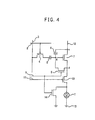
- Fig. 4 is a circuit diagram for explaining a driving circuit to suppress a noise current according to Embodiment 3 of the present invention.
- the third control signal line 15 and the first control signal line 9 in Fig. 1 are shared.
- the driving circuit in Fig. 4 is operated based on a waveform diagram for explaining an operation timing of Fig. 10.
- a fifth transistor 14 is conducted for a period in which a pixel is selected, and moreover for a period from a time before a third transistor 8 is brought into a conduction state to a time after a fourth transistor 10 is brought into a non-conduction state. Therefore, the same effects as those in Embodiment 1 can be obtained. Furthermore, it is possible to obtain an effect that the number of the signal lines is decreased and a circuit structure can be thereby prevented from being complicated.
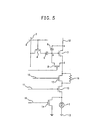
- Fig. 5 is a circuit diagram for explaining a driving circuit to suppress a noise current according to Embodiment 4 of the present invention.
- a resistive element 16 is inserted between the second transistor 7 and the fourth transistor 10 in Fig. 1, and a sixth transistor 17 is connected in parallel with the resistive element 16.
- the driving circuit in Fig. 5 is operated based on the timing chart of Fig. 2 and the sixth transistor 17 is brought into a non-conduction state for a period in which at least a fifth transistor 14 is set in a conduction state, and is brought into the conduction state for other periods.
- Fig. 6 is a circuit diagram for explaining a driving circuit to suppress a noise current, illustrating Embodiment 5 according to the present invention.
- a resistive element 16 is inserted between an organic electroluminescence element 1 and the fourth transistor 10, and a sixth transistor 17 is connected in parallel with the resistive element 16.
- the driving circuit in Fig. 6 is operated based on the timing chart of Fig. 2, and the sixth transistor 17 is brought into a non-conduction state for a period in which at least a fifth transistor 14 is set in a conduction state, and is brought into the conduction state for the other periods.
- the sixth transistor 17 might be an N channel FET if the fifth transistor 14 is a P channel FET, or the sixth transistor 17 might be the P channel FET if the fifth transistor 14 is the N channel FET.
- the fourth control signal line 18 can be shared with the third control signal line 15 in Figs. 5 and 6. Consequently, it is possible to decrease the number of the control signal lines.
- this structure can also be applied to Embodiment 2 or Embodiment 3.
- organic electroluminescence element has been taken as an example of an electroluminescence element in the description of Embodiments 2 to 4, it is possible to obtain the same effects by using another spontaneous light emitting element such as an inorganic EL.
- the present invention has a feature that a noise current flowing in a light emitting element can be suppressed so that precision in a luminance can be enhanced.
- the present invention can be utilized effectively for a spontaneous light emitting type display device.
Landscapes
- Engineering & Computer Science (AREA)
- Physics & Mathematics (AREA)
- Computer Hardware Design (AREA)
- General Physics & Mathematics (AREA)
- Theoretical Computer Science (AREA)
- Control Of Indicators Other Than Cathode Ray Tubes (AREA)
- Control Of El Displays (AREA)
- Electroluminescent Light Sources (AREA)
Applications Claiming Priority (5)
| Application Number | Priority Date | Filing Date | Title |
|---|---|---|---|
| JP2001080427 | 2001-03-21 | ||
| JP2001080427 | 2001-03-21 | ||
| JP2001253989 | 2001-08-24 | ||
| JP2001253989A JP2002351401A (ja) | 2001-03-21 | 2001-08-24 | 自発光型表示装置 |
| PCT/JP2002/002496 WO2002075712A1 (en) | 2001-03-21 | 2002-03-15 | Self-luminous display |
Publications (2)
| Publication Number | Publication Date |
|---|---|
| EP1372132A1 true EP1372132A1 (de) | 2003-12-17 |
| EP1372132A4 EP1372132A4 (de) | 2008-05-28 |
Family
ID=26611653
Family Applications (1)
| Application Number | Title | Priority Date | Filing Date |
|---|---|---|---|
| EP02705254A Withdrawn EP1372132A4 (de) | 2001-03-21 | 2002-03-15 | Selbstleuchtende anzeige |
Country Status (7)
| Country | Link |
|---|---|
| US (1) | US7154454B2 (de) |
| EP (1) | EP1372132A4 (de) |
| JP (1) | JP2002351401A (de) |
| KR (1) | KR100450809B1 (de) |
| CN (1) | CN1227638C (de) |
| TW (1) | TW533398B (de) |
| WO (1) | WO2002075712A1 (de) |
Cited By (4)
| Publication number | Priority date | Publication date | Assignee | Title |
|---|---|---|---|---|
| CN100524425C (zh) * | 2004-05-06 | 2009-08-05 | 友达光电股份有限公司 | 发光装置的驱动装置、方法 |
| US7710366B2 (en) | 2004-05-20 | 2010-05-04 | Samsung Electronics Co., Ltd. | Display device and driving method thereof |
| US7940239B2 (en) | 2002-12-27 | 2011-05-10 | Semiconductor Energy Laboratory Co., Ltd. | Semiconductor device and display device utilizing the same |
| US8378356B2 (en) | 2001-10-24 | 2013-02-19 | Semiconductor Energy Laboratory Co., Ltd. | Display device including pixel |
Families Citing this family (132)
| Publication number | Priority date | Publication date | Assignee | Title |
|---|---|---|---|---|
| KR100637433B1 (ko) | 2004-05-24 | 2006-10-20 | 삼성에스디아이 주식회사 | 발광 표시 장치 |
| JP2003108067A (ja) * | 2001-09-28 | 2003-04-11 | Sanyo Electric Co Ltd | 表示装置 |
| JP4498669B2 (ja) | 2001-10-30 | 2010-07-07 | 株式会社半導体エネルギー研究所 | 半導体装置、表示装置、及びそれらを具備する電子機器 |
| US20030103022A1 (en) * | 2001-11-09 | 2003-06-05 | Yukihiro Noguchi | Display apparatus with function for initializing luminance data of optical element |
| JP2003195809A (ja) * | 2001-12-28 | 2003-07-09 | Matsushita Electric Ind Co Ltd | El表示装置とその駆動方法および情報表示装置 |
| US9153168B2 (en) * | 2002-07-09 | 2015-10-06 | Semiconductor Energy Laboratory Co., Ltd. | Method for deciding duty factor in driving light-emitting device and driving method using the duty factor |
| JP4416456B2 (ja) * | 2002-09-02 | 2010-02-17 | キヤノン株式会社 | エレクトロルミネッセンス装置 |
| JP3832415B2 (ja) | 2002-10-11 | 2006-10-11 | ソニー株式会社 | アクティブマトリクス型表示装置 |
| TWI470607B (zh) | 2002-11-29 | 2015-01-21 | Semiconductor Energy Lab | A current driving circuit and a display device using the same |
| JP5137294B2 (ja) * | 2002-12-19 | 2013-02-06 | 株式会社半導体エネルギー研究所 | 発光装置の駆動方法 |
| KR100899082B1 (ko) * | 2002-12-30 | 2009-05-25 | 매그나칩 반도체 유한회사 | 휘도가 개선된 유기전계 발광표시장치 |
| JP4048969B2 (ja) | 2003-02-12 | 2008-02-20 | セイコーエプソン株式会社 | 電気光学装置の駆動方法及び電子機器 |
| CN100418123C (zh) * | 2003-02-24 | 2008-09-10 | 奇美电子股份有限公司 | 显示装置 |
| CN102360538B (zh) | 2003-02-28 | 2015-09-02 | 株式会社半导体能源研究所 | 半导体装置及其驱动方法 |
| US7612749B2 (en) * | 2003-03-04 | 2009-11-03 | Chi Mei Optoelectronics Corporation | Driving circuits for displays |
| TWI230914B (en) * | 2003-03-12 | 2005-04-11 | Au Optronics Corp | Circuit of current driving active matrix organic light emitting diode pixel and driving method thereof |
| JP4197287B2 (ja) * | 2003-03-28 | 2008-12-17 | シャープ株式会社 | 表示装置 |
| JP2004318093A (ja) * | 2003-03-31 | 2004-11-11 | Sanyo Electric Co Ltd | 発光ディスプレイ及びその駆動方法及びエレクトロルミネッセンス表示回路及びエレクトロルミネッセンスディスプレイ |
| KR20040089256A (ko) * | 2003-04-11 | 2004-10-21 | 윈텍 코포레이숀 | 균일한 휘도의 액티브 매트릭스 oled 디스플레이장치를 달성하기 위한 방법 및 장치 |
| KR100515299B1 (ko) * | 2003-04-30 | 2005-09-15 | 삼성에스디아이 주식회사 | 화상 표시 장치와 그 표시 패널 및 구동 방법 |
| JP4484451B2 (ja) * | 2003-05-16 | 2010-06-16 | 奇美電子股▲ふん▼有限公司 | 画像表示装置 |
| JP4016962B2 (ja) * | 2003-05-19 | 2007-12-05 | セイコーエプソン株式会社 | 電気光学装置、電気光学装置の駆動方法 |
| JP4168836B2 (ja) | 2003-06-03 | 2008-10-22 | ソニー株式会社 | 表示装置 |
| JP4062179B2 (ja) * | 2003-06-04 | 2008-03-19 | ソニー株式会社 | 画素回路、表示装置、および画素回路の駆動方法 |
| TWI253614B (en) * | 2003-06-20 | 2006-04-21 | Sanyo Electric Co | Display device |
| KR100497725B1 (ko) * | 2003-08-22 | 2005-06-23 | 삼성전자주식회사 | 디스플레이용 신호 처리 장치 및 그 방법 |
| US7408195B2 (en) * | 2003-09-04 | 2008-08-05 | Cypress Semiconductor Corporation (Belgium) Bvba | Semiconductor pixel arrays with reduced sensitivity to defects |
| KR100514183B1 (ko) | 2003-09-08 | 2005-09-13 | 삼성에스디아이 주식회사 | 유기 전계발광 표시장치의 픽셀구동회로 및 그 구동방법 |
| KR100560468B1 (ko) | 2003-09-16 | 2006-03-13 | 삼성에스디아이 주식회사 | 화상 표시 장치와 그 표시 패널 |
| JP4059177B2 (ja) * | 2003-09-17 | 2008-03-12 | セイコーエプソン株式会社 | 電子回路、その駆動方法、電気光学装置および電子機器 |
| JP2005123591A (ja) * | 2003-09-25 | 2005-05-12 | Rohm Co Ltd | 半導体装置及びこれを実装した電子機器 |
| KR100515306B1 (ko) | 2003-10-29 | 2005-09-15 | 삼성에스디아이 주식회사 | 유기el 표시패널 |
| KR100529077B1 (ko) | 2003-11-13 | 2005-11-15 | 삼성에스디아이 주식회사 | 화상 표시 장치, 그 표시 패널 및 그 구동 방법 |
| JP4297438B2 (ja) * | 2003-11-24 | 2009-07-15 | 三星モバイルディスプレイ株式會社 | 発光表示装置,表示パネル,及び発光表示装置の駆動方法 |
| KR100599726B1 (ko) * | 2003-11-27 | 2006-07-12 | 삼성에스디아이 주식회사 | 발광 표시 장치 및 그 표시 패널과 구동 방법 |
| KR100536235B1 (ko) * | 2003-11-24 | 2005-12-12 | 삼성에스디아이 주식회사 | 화상 표시 장치 및 그 구동 방법 |
| JP4147410B2 (ja) * | 2003-12-02 | 2008-09-10 | ソニー株式会社 | トランジスタ回路、画素回路、表示装置及びこれらの駆動方法 |
| US7595775B2 (en) * | 2003-12-19 | 2009-09-29 | Semiconductor Energy Laboratory Co., Ltd. | Light emitting display device with reverse biasing circuit |
| JP4547605B2 (ja) * | 2004-01-19 | 2010-09-22 | ソニー株式会社 | 表示装置及びその駆動方法 |
| US7173585B2 (en) * | 2004-03-10 | 2007-02-06 | Wintek Corporation | Active matrix display driving circuit |
| TW200540774A (en) * | 2004-04-12 | 2005-12-16 | Sanyo Electric Co | Organic EL pixel circuit |
| KR100637431B1 (ko) | 2004-04-29 | 2006-10-20 | 삼성에스디아이 주식회사 | 발광 표시 패널 및 발광 표시 장치 |
| TWI288900B (en) * | 2004-04-30 | 2007-10-21 | Fujifilm Corp | Active matrix type display device |
| CN100481180C (zh) * | 2004-05-20 | 2009-04-22 | 京瓷株式会社 | 图象显示装置及其驱动方法 |
| WO2005114629A1 (ja) | 2004-05-20 | 2005-12-01 | Kyocera Corporation | 画像表示装置およびその駆動方法 |
| US8760374B2 (en) * | 2004-05-21 | 2014-06-24 | Semiconductor Energy Laboratory Co., Ltd. | Display device having a light emitting element |
| KR100578812B1 (ko) * | 2004-06-29 | 2006-05-11 | 삼성에스디아이 주식회사 | 발광 표시 장치 |
| JP4635542B2 (ja) * | 2004-09-28 | 2011-02-23 | ソニー株式会社 | 画素回路及び表示装置 |
| KR100612392B1 (ko) | 2004-10-13 | 2006-08-16 | 삼성에스디아이 주식회사 | 발광 표시 장치 및 발광 표시 패널 |
| TWI284869B (en) * | 2004-10-22 | 2007-08-01 | Au Optronics Corp | Pixel of display |
| KR100592646B1 (ko) * | 2004-11-08 | 2006-06-26 | 삼성에스디아이 주식회사 | 발광 표시장치 및 그의 구동방법 |
| KR100592644B1 (ko) * | 2004-11-08 | 2006-06-26 | 삼성에스디아이 주식회사 | 발광 표시장치 및 그의 구동방법 |
| EP2383721B1 (de) * | 2004-11-16 | 2015-04-08 | Ignis Innovation Inc. | System und Ansteuerungsverfahren der Anzeige einer lichtemittierenden Aktivmatrix-Vorrichtung |
| KR100599788B1 (ko) * | 2004-11-17 | 2006-07-12 | 삼성에스디아이 주식회사 | 발광 표시 패널 및 발광 표시 장치 |
| KR100688801B1 (ko) | 2004-11-22 | 2007-03-02 | 삼성에스디아이 주식회사 | 델타 화소회로 및 발광 표시장치 |
| CA2490858A1 (en) | 2004-12-07 | 2006-06-07 | Ignis Innovation Inc. | Driving method for compensated voltage-programming of amoled displays |
| KR100805542B1 (ko) * | 2004-12-24 | 2008-02-20 | 삼성에스디아이 주식회사 | 발광 표시장치 및 그의 구동방법 |
| KR100637203B1 (ko) * | 2005-01-07 | 2006-10-23 | 삼성에스디아이 주식회사 | 유기 전계발광 표시장치 및 그 동작방법 |
| JP4850422B2 (ja) * | 2005-01-31 | 2012-01-11 | パイオニア株式会社 | 表示装置およびその駆動方法 |
| JP5417598B2 (ja) * | 2005-03-25 | 2014-02-19 | 国立大学法人富山大学 | 多機能有機ダイオードマトリクスパネル |
| JP5392963B2 (ja) * | 2005-04-19 | 2014-01-22 | インテレクチュアル キーストーン テクノロジー エルエルシー | 電気光学装置及び電子機器 |
| TW200701167A (en) * | 2005-04-15 | 2007-01-01 | Seiko Epson Corp | Electronic circuit, and driving method, electrooptical device, and electronic apparatus thereof |
| JP2006300980A (ja) * | 2005-04-15 | 2006-11-02 | Seiko Epson Corp | 電子回路、その駆動方法、電気光学装置、及び電子機器 |
| CN100405444C (zh) * | 2005-04-22 | 2008-07-23 | 中国科学院长春光学精密机械与物理研究所 | 一种有机电致发光显示的驱动方法 |
| TWI302281B (en) * | 2005-05-23 | 2008-10-21 | Au Optronics Corp | Display unit, display array, display panel and display unit control method |
| CN102663977B (zh) | 2005-06-08 | 2015-11-18 | 伊格尼斯创新有限公司 | 用于驱动发光器件显示器的方法和系统 |
| WO2006137295A1 (ja) * | 2005-06-23 | 2006-12-28 | Sharp Kabushiki Kaisha | 表示装置およびその駆動方法 |
| TW200709160A (en) | 2005-07-20 | 2007-03-01 | Pioneer Corp | Active matrix type display device |
| JP4788216B2 (ja) * | 2005-07-21 | 2011-10-05 | コニカミノルタホールディングス株式会社 | 駆動装置および表示装置ならびに駆動装置および表示装置の駆動方法 |
| KR100985860B1 (ko) * | 2005-11-08 | 2010-10-08 | 삼성전자주식회사 | 발광장치 및 그 제어방법 |
| KR101214205B1 (ko) | 2005-12-02 | 2012-12-21 | 재단법인서울대학교산학협력재단 | 표시 장치 및 그 구동 방법 |
| US9269322B2 (en) | 2006-01-09 | 2016-02-23 | Ignis Innovation Inc. | Method and system for driving an active matrix display circuit |
| US9489891B2 (en) | 2006-01-09 | 2016-11-08 | Ignis Innovation Inc. | Method and system for driving an active matrix display circuit |
| WO2007079572A1 (en) | 2006-01-09 | 2007-07-19 | Ignis Innovation Inc. | Method and system for driving an active matrix display circuit |
| US8599111B2 (en) * | 2006-03-10 | 2013-12-03 | Canon Kabushiki Kaisha | Driving circuit of display element and image display apparatus |
| KR100893616B1 (ko) * | 2006-04-17 | 2009-04-20 | 삼성모바일디스플레이주식회사 | 전자 영상 기기, 2d/3d 영상 표시 장치 및 그 구동방법 |
| JP4882536B2 (ja) * | 2006-06-19 | 2012-02-22 | セイコーエプソン株式会社 | 電子回路及び電子機器 |
| KR101279115B1 (ko) * | 2006-06-27 | 2013-06-26 | 엘지디스플레이 주식회사 | 유기전계발광표시장치의 화소 회로 |
| JP4208902B2 (ja) * | 2006-06-30 | 2009-01-14 | キヤノン株式会社 | アクティブマトリクス型表示装置およびその駆動方法 |
| TWI442368B (zh) * | 2006-10-26 | 2014-06-21 | Semiconductor Energy Lab | 電子裝置,顯示裝置,和半導體裝置,以及其驅動方法 |
| GB0721567D0 (en) * | 2007-11-02 | 2007-12-12 | Cambridge Display Tech Ltd | Pixel driver circuits |
| US20110199356A1 (en) * | 2007-12-06 | 2011-08-18 | Pioneer Corporation | Pixel circuit and display panel |
| KR20090106162A (ko) * | 2008-04-04 | 2009-10-08 | 삼성모바일디스플레이주식회사 | 유기 발광 표시장치 및 그 구동방법 |
| TW200949807A (en) | 2008-04-18 | 2009-12-01 | Ignis Innovation Inc | System and driving method for light emitting device display |
| CA2637343A1 (en) | 2008-07-29 | 2010-01-29 | Ignis Innovation Inc. | Improving the display source driver |
| KR101509113B1 (ko) | 2008-12-05 | 2015-04-08 | 삼성디스플레이 주식회사 | 표시 장치 및 그 구동 방법 |
| US9370075B2 (en) | 2008-12-09 | 2016-06-14 | Ignis Innovation Inc. | System and method for fast compensation programming of pixels in a display |
| JP5287210B2 (ja) * | 2008-12-17 | 2013-09-11 | ソニー株式会社 | 表示装置および電子機器 |
| US8633873B2 (en) | 2009-11-12 | 2014-01-21 | Ignis Innovation Inc. | Stable fast programming scheme for displays |
| CA2687631A1 (en) | 2009-12-06 | 2011-06-06 | Ignis Innovation Inc | Low power driving scheme for display applications |
| CA2696778A1 (en) | 2010-03-17 | 2011-09-17 | Ignis Innovation Inc. | Lifetime, uniformity, parameter extraction methods |
| TWI493524B (zh) | 2010-06-10 | 2015-07-21 | Prime View Int Co Ltd | 發光顯示器的畫素驅動電路及相關裝置與方法 |
| JP5982147B2 (ja) | 2011-04-01 | 2016-08-31 | 株式会社半導体エネルギー研究所 | 発光装置 |
| US8922464B2 (en) | 2011-05-11 | 2014-12-30 | Semiconductor Energy Laboratory Co., Ltd. | Active matrix display device and driving method thereof |
| US9886899B2 (en) | 2011-05-17 | 2018-02-06 | Ignis Innovation Inc. | Pixel Circuits for AMOLED displays |
| US9351368B2 (en) | 2013-03-08 | 2016-05-24 | Ignis Innovation Inc. | Pixel circuits for AMOLED displays |
| US20140368491A1 (en) | 2013-03-08 | 2014-12-18 | Ignis Innovation Inc. | Pixel circuits for amoled displays |
| CN102708785B (zh) * | 2011-05-18 | 2015-06-24 | 京东方科技集团股份有限公司 | 像素单元电路及其工作方法、oled显示装置 |
| EP2715711A4 (de) | 2011-05-28 | 2014-12-24 | Ignis Innovation Inc | System und verfahren zur schnellen kompensationsprogrammierung von pixeln auf einer anzeige |
| US8710505B2 (en) | 2011-08-05 | 2014-04-29 | Semiconductor Energy Laboratory Co., Ltd. | Semiconductor device |
| KR101396004B1 (ko) * | 2011-08-17 | 2014-05-16 | 엘지디스플레이 주식회사 | 유기발광다이오드 표시장치 |
| JP6050054B2 (ja) | 2011-09-09 | 2016-12-21 | 株式会社半導体エネルギー研究所 | 半導体装置 |
| KR102358737B1 (ko) | 2011-10-18 | 2022-02-08 | 가부시키가이샤 한도오따이 에네루기 켄큐쇼 | 발광 장치 |
| US12176356B2 (en) | 2011-10-18 | 2024-12-24 | Semiconductor Energy Laboratory Co., Ltd. | Semiconductor device including transistor and light-emitting element |
| TWI451384B (zh) * | 2011-12-30 | 2014-09-01 | Au Optronics Corp | 像素結構、其驅動方法及使用其之自發光顯示器 |
| TWI460704B (zh) * | 2012-03-21 | 2014-11-11 | Innocom Tech Shenzhen Co Ltd | 顯示器及其驅動方法 |
| US10043794B2 (en) | 2012-03-22 | 2018-08-07 | Semiconductor Energy Laboratory Co., Ltd. | Semiconductor device and electronic device |
| US9747834B2 (en) | 2012-05-11 | 2017-08-29 | Ignis Innovation Inc. | Pixel circuits including feedback capacitors and reset capacitors, and display systems therefore |
| JP6228753B2 (ja) * | 2012-06-01 | 2017-11-08 | 株式会社半導体エネルギー研究所 | 半導体装置、表示装置、表示モジュール、及び電子機器 |
| US9336717B2 (en) | 2012-12-11 | 2016-05-10 | Ignis Innovation Inc. | Pixel circuits for AMOLED displays |
| US9786223B2 (en) | 2012-12-11 | 2017-10-10 | Ignis Innovation Inc. | Pixel circuits for AMOLED displays |
| TW201426709A (zh) * | 2012-12-26 | 2014-07-01 | Sony Corp | 顯示裝置、顯示裝置之驅動方法及電子機器 |
| CA2894717A1 (en) | 2015-06-19 | 2016-12-19 | Ignis Innovation Inc. | Optoelectronic device characterization in array with shared sense line |
| US9721505B2 (en) | 2013-03-08 | 2017-08-01 | Ignis Innovation Inc. | Pixel circuits for AMOLED displays |
| JP2015014764A (ja) * | 2013-07-08 | 2015-01-22 | ソニー株式会社 | 表示装置、表示装置の駆動方法、及び、電子機器 |
| JP6164059B2 (ja) | 2013-11-15 | 2017-07-19 | ソニー株式会社 | 表示装置、電子機器、及び表示装置の駆動方法 |
| CN103700346B (zh) * | 2013-12-27 | 2016-08-31 | 合肥京东方光电科技有限公司 | 像素驱动电路、阵列基板、显示装置和像素驱动方法 |
| CA2873476A1 (en) | 2014-12-08 | 2016-06-08 | Ignis Innovation Inc. | Smart-pixel display architecture |
| CA2886862A1 (en) | 2015-04-01 | 2016-10-01 | Ignis Innovation Inc. | Adjusting display brightness for avoiding overheating and/or accelerated aging |
| US10657895B2 (en) | 2015-07-24 | 2020-05-19 | Ignis Innovation Inc. | Pixels and reference circuits and timing techniques |
| US10373554B2 (en) | 2015-07-24 | 2019-08-06 | Ignis Innovation Inc. | Pixels and reference circuits and timing techniques |
| CA2898282A1 (en) | 2015-07-24 | 2017-01-24 | Ignis Innovation Inc. | Hybrid calibration of current sources for current biased voltage progra mmed (cbvp) displays |
| CA2908285A1 (en) | 2015-10-14 | 2017-04-14 | Ignis Innovation Inc. | Driver with multiple color pixel structure |
| CN106205491B (zh) * | 2016-07-11 | 2018-09-11 | 京东方科技集团股份有限公司 | 一种像素电路、其驱动方法及相关装置 |
| CN106997747B (zh) * | 2017-05-27 | 2019-01-01 | 京东方科技集团股份有限公司 | 一种有机发光显示面板及显示装置 |
| EP3525251A1 (de) * | 2018-02-09 | 2019-08-14 | Koninklijke Philips N.V. | Aktuatorvorrichtung mit stromadressiertem elektroaktivem polymer |
| CN110473496B (zh) * | 2018-05-09 | 2021-01-26 | 京东方科技集团股份有限公司 | 像素电路及其驱动方法、显示基板、显示装置 |
| CN109979377B (zh) * | 2018-06-27 | 2021-01-15 | 友达光电股份有限公司 | 像素电路与显示装置 |
| CN110544459B (zh) * | 2019-09-10 | 2022-01-04 | 信利(惠州)智能显示有限公司 | 像素电路及其驱动方法以及显示装置 |
| CN113838415B (zh) | 2020-06-08 | 2023-01-17 | 京东方科技集团股份有限公司 | 像素驱动电路及其驱动方法、显示面板及显示装置 |
| CN114822396B (zh) * | 2022-05-12 | 2023-01-10 | 惠科股份有限公司 | 像素驱动电路和显示面板 |
| WO2024174153A1 (zh) | 2023-02-23 | 2024-08-29 | 京东方科技集团股份有限公司 | 像素电路、像素驱动方法和显示装置 |
Family Cites Families (18)
| Publication number | Priority date | Publication date | Assignee | Title |
|---|---|---|---|---|
| USRE31872E (en) * | 1974-04-25 | 1985-04-23 | Timex Corporation | Electro-optical display with circuitry for applying predetermined potentials to all display segments to effect activation of a selected segment only |
| JPH0758635B2 (ja) * | 1989-11-24 | 1995-06-21 | 富士ゼロックス株式会社 | El駆動回路 |
| DE69825402T2 (de) | 1997-03-12 | 2005-08-04 | Seiko Epson Corp. | Pixelschaltung, anzeigevorrichtung und elektronische apparatur mit stromgesteuerter lichtemittierender vorrichtung |
| WO1998048403A1 (en) * | 1997-04-23 | 1998-10-29 | Sarnoff Corporation | Active matrix light emitting diode pixel structure and method |
| JP3259774B2 (ja) * | 1999-06-09 | 2002-02-25 | 日本電気株式会社 | 画像表示方法および装置 |
| JP5210473B2 (ja) | 1999-06-21 | 2013-06-12 | 株式会社半導体エネルギー研究所 | 表示装置 |
| JP4627822B2 (ja) * | 1999-06-23 | 2011-02-09 | 株式会社半導体エネルギー研究所 | 表示装置 |
| US6859193B1 (en) * | 1999-07-14 | 2005-02-22 | Sony Corporation | Current drive circuit and display device using the same, pixel circuit, and drive method |
| JP2001056667A (ja) * | 1999-08-18 | 2001-02-27 | Tdk Corp | 画像表示装置 |
| JP2001075524A (ja) | 1999-09-03 | 2001-03-23 | Rohm Co Ltd | 表示装置 |
| JP2001083924A (ja) * | 1999-09-08 | 2001-03-30 | Matsushita Electric Ind Co Ltd | 電流制御型発光素子の駆動回路および駆動方法 |
| JP4145495B2 (ja) * | 2000-01-11 | 2008-09-03 | 株式会社半導体エネルギー研究所 | 表示装置、コンピュータ、ビデオカメラ、デジタルカメラ、ゴーグル型ディスプレイ、ナビゲーションシステム、音響再生装置、ゲーム機器、携帯情報端末、及び画像再生装置 |
| TW480727B (en) | 2000-01-11 | 2002-03-21 | Semiconductor Energy Laboratro | Semiconductor display device |
| JP4112184B2 (ja) | 2000-01-31 | 2008-07-02 | 株式会社半導体エネルギー研究所 | エリアセンサ及び表示装置 |
| US6747638B2 (en) | 2000-01-31 | 2004-06-08 | Semiconductor Energy Laboratory Co., Ltd. | Adhesion type area sensor and display device having adhesion type area sensor |
| TW548621B (en) * | 2000-12-08 | 2003-08-21 | Matsushita Electric Industrial Co Ltd | EL display device |
| US7209101B2 (en) * | 2001-08-29 | 2007-04-24 | Nec Corporation | Current load device and method for driving the same |
| US7365713B2 (en) * | 2001-10-24 | 2008-04-29 | Semiconductor Energy Laboratory Co., Ltd. | Semiconductor device and driving method thereof |
-
2001
- 2001-08-24 JP JP2001253989A patent/JP2002351401A/ja active Pending
-
2002
- 2002-03-15 US US10/276,159 patent/US7154454B2/en not_active Expired - Lifetime
- 2002-03-15 WO PCT/JP2002/002496 patent/WO2002075712A1/ja not_active Ceased
- 2002-03-15 KR KR10-2002-7015634A patent/KR100450809B1/ko not_active Expired - Fee Related
- 2002-03-15 EP EP02705254A patent/EP1372132A4/de not_active Withdrawn
- 2002-03-15 CN CNB028007875A patent/CN1227638C/zh not_active Expired - Fee Related
- 2002-03-18 TW TW091105025A patent/TW533398B/zh not_active IP Right Cessation
Non-Patent Citations (2)
| Title |
|---|
| DAWSON R M A ET AL: "The impact of the transient response of organic light emitting diodes on the design of active matrix OLED displays" 6 December 1998 (1998-12-06), ELECTRON DEVICES MEETING, 1998. IEDM '98 TECHNICAL DIGEST., INTERNATIONAL SAN FRANCISCO, CA, USA 6-9 DEC. 1998, PISCATAWAY, NJ, USA,IEEE, US, PAGE(S) 875-878 , XP010321598 ISBN: 0-7803-4774-9 * figure 9 * * |
| See also references of WO02075712A1 * |
Cited By (12)
| Publication number | Priority date | Publication date | Assignee | Title |
|---|---|---|---|---|
| US8378356B2 (en) | 2001-10-24 | 2013-02-19 | Semiconductor Energy Laboratory Co., Ltd. | Display device including pixel |
| US8659027B2 (en) | 2001-10-24 | 2014-02-25 | Semiconductor Energy Laboratory Co., Ltd. | Semiconductor device and electronic device |
| US8994029B2 (en) | 2001-10-24 | 2015-03-31 | Semiconductor Energy Laboratory Co., Ltd. | Semiconductor device and driving method thereof |
| US9082734B2 (en) | 2001-10-24 | 2015-07-14 | Semiconductor Energy Laboratory Co., Ltd. | Semiconductor device and driving method thereof |
| US9449549B2 (en) | 2001-10-24 | 2016-09-20 | Semiconductor Energy Laboratory Co., Ltd. | Semiconductor device and driving method thereof |
| US9892679B2 (en) | 2001-10-24 | 2018-02-13 | Semiconductor Energy Laboratory Co., Ltd. | Display device |
| US10679550B2 (en) | 2001-10-24 | 2020-06-09 | Semiconductor Energy Laboratory Co., Ltd. | Display device |
| US7940239B2 (en) | 2002-12-27 | 2011-05-10 | Semiconductor Energy Laboratory Co., Ltd. | Semiconductor device and display device utilizing the same |
| US8866714B2 (en) | 2002-12-27 | 2014-10-21 | Semiconductor Energy Laboratory Co., Ltd. | Semiconductor device and display device utilizing the same |
| US9620060B2 (en) | 2002-12-27 | 2017-04-11 | Semiconductor Energy Laboratory Co., Ltd. | Semiconductor device including transistors, switches and capacitor, and electronic device utilizing the same |
| CN100524425C (zh) * | 2004-05-06 | 2009-08-05 | 友达光电股份有限公司 | 发光装置的驱动装置、方法 |
| US7710366B2 (en) | 2004-05-20 | 2010-05-04 | Samsung Electronics Co., Ltd. | Display device and driving method thereof |
Also Published As
| Publication number | Publication date |
|---|---|
| KR20030001530A (ko) | 2003-01-06 |
| WO2002075712A1 (en) | 2002-09-26 |
| EP1372132A4 (de) | 2008-05-28 |
| CN1227638C (zh) | 2005-11-16 |
| TW533398B (en) | 2003-05-21 |
| JP2002351401A (ja) | 2002-12-06 |
| CN1460240A (zh) | 2003-12-03 |
| US20030112208A1 (en) | 2003-06-19 |
| US7154454B2 (en) | 2006-12-26 |
| KR100450809B1 (ko) | 2004-10-01 |
Similar Documents
| Publication | Publication Date | Title |
|---|---|---|
| EP1372132A1 (de) | Selbstleuchtende anzeige | |
| US11282462B2 (en) | Electronic display with hybrid in-pixel and external compensation | |
| US7061452B2 (en) | Spontaneous light-emitting display device | |
| US6841948B2 (en) | Device for driving luminescent display panel | |
| EP1646032B1 (de) | Pixelschaltung für ein OLED Display mit automatischer Kompensation der Schwellenspannung | |
| KR101157979B1 (ko) | 유기발광다이오드 구동회로와 이를 이용한유기발광다이오드 표시장치 | |
| CN100452152C (zh) | 像素电路、显示设备以及驱动像素电路的方法 | |
| US7187350B2 (en) | Active type light emitting display device | |
| CN105513539B (zh) | 像素电路及其驱动方法以及显示装置 | |
| JP4070696B2 (ja) | 発光表示装置,発光表示装置の駆動方法,および発光表示装置の表示パネル | |
| CN118015973A (zh) | 一种显示面板、驱动方法及显示装置 | |
| US8692746B2 (en) | Image display device for reducing the amount of time required to perform plural, consecutive threshold voltage correction operations | |
| US20090244051A1 (en) | Self light emitting type display device | |
| KR101139527B1 (ko) | 유기전계발광소자 및 유기전계발광 표시장치 | |
| US20040130513A1 (en) | Method of driving electronic circuit, method of driving electronic apparatus, method of driving electro-optical apparatus, and electronic device | |
| KR20060136067A (ko) | 유기전계발광소자 및 유기전계발광 표시장치 | |
| KR100628277B1 (ko) | 유기전계발광표시장치 및 이의 구동방법 | |
| JP2004279548A (ja) | 表示駆動方法およびその回路ならびに画像表示装置 | |
| US20060007070A1 (en) | Driving circuit and driving method for electroluminescent display | |
| CN114203115A (zh) | 驱动电压补偿电路、驱动电路、像素驱动电路及显示装置 | |
| KR101137849B1 (ko) | 발광 표시장치 | |
| US20060007078A1 (en) | Active matrix organic light emitting diode (AMOLED) display panel and a driving circuit thereof | |
| KR101478096B1 (ko) | 전압보상형 화소회로 및 그 구동방법 | |
| JP2007322795A (ja) | 発光ダイオード駆動回路およびそれを使用した表示装置 | |
| US7212179B2 (en) | Light emitting display device, electronic equipment into which the same device is loaded, and drive method of the light emitting display device |
Legal Events
| Date | Code | Title | Description |
|---|---|---|---|
| PUAI | Public reference made under article 153(3) epc to a published international application that has entered the european phase |
Free format text: ORIGINAL CODE: 0009012 |
|
| 17P | Request for examination filed |
Effective date: 20021216 |
|
| AK | Designated contracting states |
Kind code of ref document: A1 Designated state(s): AT BE CH CY DE DK ES FI FR GB GR IE IT LI LU MC NL PT SE TR |
|
| AX | Request for extension of the european patent |
Extension state: AL LT LV MK RO SI |
|
| RAP1 | Party data changed (applicant data changed or rights of an application transferred) |
Owner name: MITSUBISHI DENKI KABUSHIKI KAISHA |
|
| A4 | Supplementary search report drawn up and despatched |
Effective date: 20080425 |
|
| 17Q | First examination report despatched |
Effective date: 20100930 |
|
| STAA | Information on the status of an ep patent application or granted ep patent |
Free format text: STATUS: THE APPLICATION HAS BEEN WITHDRAWN |
|
| 18W | Application withdrawn |
Effective date: 20110124 |