EP1383157A2 - Elektronenstrahlbelichtungsverfahren und Verfahren zur Herstellung einer Halbleitervorrichtung - Google Patents
Elektronenstrahlbelichtungsverfahren und Verfahren zur Herstellung einer Halbleitervorrichtung Download PDFInfo
- Publication number
- EP1383157A2 EP1383157A2 EP03254452A EP03254452A EP1383157A2 EP 1383157 A2 EP1383157 A2 EP 1383157A2 EP 03254452 A EP03254452 A EP 03254452A EP 03254452 A EP03254452 A EP 03254452A EP 1383157 A2 EP1383157 A2 EP 1383157A2
- Authority
- EP
- European Patent Office
- Prior art keywords
- stage
- substrate
- axis
- substrate stage
- tilt frame
- Prior art date
- Legal status (The legal status is an assumption and is not a legal conclusion. Google has not performed a legal analysis and makes no representation as to the accuracy of the status listed.)
- Withdrawn
Links
- 238000010894 electron beam technology Methods 0.000 title claims abstract description 77
- 239000004065 semiconductor Substances 0.000 title claims description 13
- 238000004519 manufacturing process Methods 0.000 title claims description 10
- 239000000758 substrate Substances 0.000 claims abstract description 61
- 238000012546 transfer Methods 0.000 claims abstract description 31
- 239000003795 chemical substances by application Substances 0.000 claims description 7
- 239000011248 coating agent Substances 0.000 claims description 4
- 238000000576 coating method Methods 0.000 claims description 4
- 238000011161 development Methods 0.000 claims description 3
- 230000005484 gravity Effects 0.000 claims 1
- 230000003287 optical effect Effects 0.000 description 31
- 230000009467 reduction Effects 0.000 description 13
- 238000000034 method Methods 0.000 description 10
- 230000004075 alteration Effects 0.000 description 9
- 238000005259 measurement Methods 0.000 description 6
- 230000015556 catabolic process Effects 0.000 description 5
- 238000006731 degradation reaction Methods 0.000 description 5
- 238000013461 design Methods 0.000 description 5
- 238000001459 lithography Methods 0.000 description 5
- 229910000889 permalloy Inorganic materials 0.000 description 4
- 230000008569 process Effects 0.000 description 4
- 238000012937 correction Methods 0.000 description 3
- XUIMIQQOPSSXEZ-UHFFFAOYSA-N Silicon Chemical compound [Si] XUIMIQQOPSSXEZ-UHFFFAOYSA-N 0.000 description 2
- 201000009310 astigmatism Diseases 0.000 description 2
- 230000015572 biosynthetic process Effects 0.000 description 2
- 238000005530 etching Methods 0.000 description 2
- 238000007689 inspection Methods 0.000 description 2
- 229910052710 silicon Inorganic materials 0.000 description 2
- 239000010703 silicon Substances 0.000 description 2
- 238000012360 testing method Methods 0.000 description 2
- 206010010071 Coma Diseases 0.000 description 1
- 230000001133 acceleration Effects 0.000 description 1
- 238000012790 confirmation Methods 0.000 description 1
- 238000006073 displacement reaction Methods 0.000 description 1
- 238000005538 encapsulation Methods 0.000 description 1
- 239000011521 glass Substances 0.000 description 1
- 238000005468 ion implantation Methods 0.000 description 1
- 150000002500 ions Chemical class 0.000 description 1
- 238000005461 lubrication Methods 0.000 description 1
- 239000000463 material Substances 0.000 description 1
- 230000007246 mechanism Effects 0.000 description 1
- 230000003647 oxidation Effects 0.000 description 1
- 238000007254 oxidation reaction Methods 0.000 description 1
- 238000012858 packaging process Methods 0.000 description 1
- 239000002245 particle Substances 0.000 description 1
- 238000012545 processing Methods 0.000 description 1
- 230000004044 response Effects 0.000 description 1
- 238000005096 rolling process Methods 0.000 description 1
- 238000007740 vapor deposition Methods 0.000 description 1
Images




Classifications
-
- H—ELECTRICITY
- H01—ELECTRIC ELEMENTS
- H01J—ELECTRIC DISCHARGE TUBES OR DISCHARGE LAMPS
- H01J37/00—Discharge tubes with provision for introducing objects or material to be exposed to the discharge, e.g. for the purpose of examination or processing thereof
- H01J37/02—Details
- H01J37/20—Means for supporting or positioning the object or the material; Means for adjusting diaphragms or lenses associated with the support
-
- B—PERFORMING OPERATIONS; TRANSPORTING
- B82—NANOTECHNOLOGY
- B82Y—SPECIFIC USES OR APPLICATIONS OF NANOSTRUCTURES; MEASUREMENT OR ANALYSIS OF NANOSTRUCTURES; MANUFACTURE OR TREATMENT OF NANOSTRUCTURES
- B82Y10/00—Nanotechnology for information processing, storage or transmission, e.g. quantum computing or single electron logic
-
- B—PERFORMING OPERATIONS; TRANSPORTING
- B82—NANOTECHNOLOGY
- B82Y—SPECIFIC USES OR APPLICATIONS OF NANOSTRUCTURES; MEASUREMENT OR ANALYSIS OF NANOSTRUCTURES; MANUFACTURE OR TREATMENT OF NANOSTRUCTURES
- B82Y40/00—Manufacture or treatment of nanostructures
-
- H—ELECTRICITY
- H01—ELECTRIC ELEMENTS
- H01J—ELECTRIC DISCHARGE TUBES OR DISCHARGE LAMPS
- H01J37/00—Discharge tubes with provision for introducing objects or material to be exposed to the discharge, e.g. for the purpose of examination or processing thereof
- H01J37/30—Electron-beam or ion-beam tubes for localised treatment of objects
- H01J37/317—Electron-beam or ion-beam tubes for localised treatment of objects for changing properties of the objects or for applying thin layers thereon, e.g. for ion implantation
- H01J37/3174—Particle-beam lithography, e.g. electron beam lithography
-
- H—ELECTRICITY
- H01—ELECTRIC ELEMENTS
- H01J—ELECTRIC DISCHARGE TUBES OR DISCHARGE LAMPS
- H01J37/00—Discharge tubes with provision for introducing objects or material to be exposed to the discharge, e.g. for the purpose of examination or processing thereof
- H01J37/30—Electron-beam or ion-beam tubes for localised treatment of objects
- H01J37/317—Electron-beam or ion-beam tubes for localised treatment of objects for changing properties of the objects or for applying thin layers thereon, e.g. for ion implantation
- H01J37/3174—Particle-beam lithography, e.g. electron beam lithography
- H01J37/3177—Multi-beam, e.g. fly's eye, comb probe
-
- H—ELECTRICITY
- H01—ELECTRIC ELEMENTS
- H01J—ELECTRIC DISCHARGE TUBES OR DISCHARGE LAMPS
- H01J2237/00—Discharge tubes exposing object to beam, e.g. for analysis treatment, etching, imaging
- H01J2237/20—Positioning, supporting, modifying or maintaining the physical state of objects being observed or treated
- H01J2237/202—Movement
- H01J2237/20214—Rotation
-
- H—ELECTRICITY
- H01—ELECTRIC ELEMENTS
- H01J—ELECTRIC DISCHARGE TUBES OR DISCHARGE LAMPS
- H01J2237/00—Discharge tubes exposing object to beam, e.g. for analysis treatment, etching, imaging
- H01J2237/20—Positioning, supporting, modifying or maintaining the physical state of objects being observed or treated
- H01J2237/202—Movement
- H01J2237/20221—Translation
- H01J2237/20228—Mechanical X-Y scanning
-
- H—ELECTRICITY
- H01—ELECTRIC ELEMENTS
- H01J—ELECTRIC DISCHARGE TUBES OR DISCHARGE LAMPS
- H01J2237/00—Discharge tubes exposing object to beam, e.g. for analysis treatment, etching, imaging
- H01J2237/20—Positioning, supporting, modifying or maintaining the physical state of objects being observed or treated
- H01J2237/202—Movement
- H01J2237/20221—Translation
- H01J2237/20235—Z movement or adjustment
-
- H—ELECTRICITY
- H01—ELECTRIC ELEMENTS
- H01J—ELECTRIC DISCHARGE TUBES OR DISCHARGE LAMPS
- H01J2237/00—Discharge tubes exposing object to beam, e.g. for analysis treatment, etching, imaging
- H01J2237/30—Electron or ion beam tubes for processing objects
- H01J2237/317—Processing objects on a microscale
- H01J2237/3175—Lithography
- H01J2237/31774—Multi-beam
Definitions
- the present invention relates to an electron beam exposure apparatus and semiconductor device manufacturing method and, more particularly, to an electron beam exposure apparatus which performs pattern drawing using electron beams and a semiconductor device manufacturing method using the same.
- a lithography technique for reducing and transferring various patterns formed on a mask onto a wafer with light is used to manufacture semiconductor devices.
- a mask pattern for use in lithography is required to have an extremely high degree of accuracy.
- an electron beam exposure apparatus capable of drawing fine patterns is employed.
- An electron beam exposure apparatus is also employed to directly draw a fine pattern on a wafer without any masks.
- Electron beam exposure apparatuses include, e.g., a point-beam type apparatus which uses spot-like beams and a variable rectangular beam type apparatus which uses beams each having a variable-size rectangular cross section.
- a general electron beam exposure apparatus comprises an electron gun portion which generates electron beams, an electron optical system for guiding electron beams emitted from the electron gun portion onto a sample, a stage system for scanning the entire surface of the sample with electron beams, and an objective deflector for positioning electron beams on the sample at high accuracy.
- a region in which the objective deflector can position electron beams needs to have a width of about several mm in order to minimize any aberrations in an electron optical system.
- the size of the sample when a silicon wafer is employed as the sample, its diameter is about 200 to 300 mm ⁇ .
- the size of a glass substrate to be used as a mask its size is about 150 mm square. For this reason, a stage which enables scanning of the entire surface of the sample with electron beams is adopted.
- any shift in posture and position of the stage are measured. Since the response of positioning electron beams is extremely high, the amount of shift is generally adjusted not by using a system arrangement for improving the mechanical and control characteristics of the stage but by positioning electron beams with a deflector which deflects the electron beams.
- a conventional stage only has to move in the direction of the X-Y plane. Additionally, a conventional stage has certain constraints, i.e., the stage must be arranged in a vacuum chamber and is not allowed to cause any variation in magnetic field, which may affect the positioning of electron beams. For this reason, a conventional stage comprises limited contact mechanism elements such as a rolling guide, ball screw actuator, and the like.
- an X-Y transfer stage comprising a stage arrangement which includes a vacuum air guide and linear motor and has two degrees of freedom in a plane direction, as shown in Fig. 5.
- a stage can accelerate extremely smoothly in the X and Y directions and the stage can be hardly disturbed by a guide in alignment in the X and Y directions.
- An electron beam exposure apparatus must have a higher speed (throughput) in lithography.
- a multi electron beam exposure apparatus which irradiates the surface of a sample with a plurality of electron beams in accordance with design coordinates, scans the sample surface by deflecting the plurality of electron beams in accordance with the design coordinates, and individually turns on/off the plurality of electron beams in accordance with a pattern to be drawn, as disclosed in Japanese Patent Laid-Open No. 9-330867.
- a multi electron beam exposure apparatus can draw an arbitrary pattern with a plurality of electron beams and thus can increase the throughput.
- Fig. 6 is a view showing the outline of a multi electron beam exposure apparatus. Electron guns 501a, 501b, and 501c can individually turn on/off electron beams.
- a reduction electron optical system 502 reduces and projects a plurality of electron beams from the electron guns 501a, 501b, and 501c onto a wafer 503.
- a deflector 504 deflects the plurality of reduced and projected electron beams onto the wafer 503.
- Fig. 7 shows how the multi electron beam exposure apparatus of Fig. 6 scans a wafer with a plurality of electron beams.
- White circles represent beam reference positions (BS1, BS2, and BS3) at which each electron beam comes incident on the wafer when it is not deflected by the deflector 504.
- the beam reference positions (BS1, BS2, and BS3) are plotted along a design orthogonal coordinate system (Xs,Ys).
- the respective electron beams move along the design orthogonal coordinate system (Xs,Ys) with reference to the beam reference positions (BS1, BS2, and BS3) and scan exposure fields (EF1, EF2, and EF3) for the respective electron beams.
- the exposure fields for the respective electron beams are arranged adjacent to each other. By sequentially exposing these exposure fields, the exposure fields over the entire wafer are exposed.
- lithography requires higher accuracy and higher speed, it is necessary to suppress a degradation in drawing accuracy due to the yawing component of a stage supporting a substrate.
- a yawing component is more likely to occur as a positional shift from each beam than by a single-beam exposure scheme such as a point-beam type exposure scheme, variable rectangular beam type exposure scheme, or the like.
- a beam position is located at the intersection point of measurement axes for measuring the position of a stage in two axial directions on a plane. For this reason, a shift in the plane direction due to a distance from the beam position regardless of the position of the rotation center of yawing is automatically corrected by position feedback. If part of the shift is left uncorrected, a deflector may correct the part as a stage positional shift. In this case, a rotation component will be left uncorrected. Assume that the size of an exposure field is 10 ⁇ m square, and that a 100- ⁇ rad stage rotates. In this case, though a positional shift of up to 1 nm may occur in the in-plane direction of a wafer within a drawing spot, this shift can be neglected.
- a multi electron beam exposure apparatus using a plurality of beams.
- the plurality of beams comprise two beams, and a distance between the beams is 10 mm, only one beam can be positioned at the intersection point of measurement axes.
- a positional shift from a beam position at the intersection point is the same as described in the case of a single-beam exposure apparatus.
- a positional shift occurs in accordance with a distance from the intersection point of the measurement axes. If a 100- ⁇ rad stage rotates with the above-mentioned beam distance, a difference between the positional shift amounts of the respective beams becomes 1000 nm.
- rotation correction may collectively be performed for all the beams by a rotary deflector or correction may separately be performed for the beams by respective deflectors.
- Either method however, inevitably has a complicated control system, thus resulting in an increase in cost and a decrease in throughput.
- At least some embodiments of the present invention seek to provide an electron beam exposure apparatus capable of reducing a degradation in drawing accuracy and performing high-accuracy exposure.
- an electron beam exposure apparatus which exposes a substrate with a predetermined pattern using one or a plurality of electron beams, comprising a substrate stage on which a substrate is mounted, a transfer stage which drives the substrate stage on an X-Y plane, and an electromagnetic actuator which drives the substrate stage in a rotation direction about a Z-axis with respect to the transfer stage.
- the electromagnetic actuator includes a movable element and a stator, the movable element is fixed on the substrate stage, and the stator is fixed on the transfer stage.
- the movable element and the stator are preferably in non-contact to each other.
- the movable element comprises a magnet
- the stator comprises a coil
- the apparatus further comprises a Z actuator for driving the substrate stage in a Z direction and a tilt frame which is supported on the transfer stage through the Z actuator, and the substrate stage is connected to the tilt frame.
- the tilt frame has a connecting member with a degree of freedom in the rotation direction about the Z-axis, and the substrate stage is supported on the tilt frame through the connecting member.
- the apparatus preferably further comprises a second electromagnetic actuator arranged between the substrate stage and the transfer stage to drive the substrate stage in at least one of a rotation direction about an X-axis, a rotation direction about a Y-axis, a Z-axis direction, and X-Y direction with respect to the transfer stage.
- a second electromagnetic actuator arranged between the substrate stage and the transfer stage to drive the substrate stage in at least one of a rotation direction about an X-axis, a rotation direction about a Y-axis, a Z-axis direction, and X-Y direction with respect to the transfer stage.
- the electromagnetic actuator comprises a plurality of electromagnetic actuators, and the plurality of electromagnetic actuators are combined to drive the substrate stage with six degrees of freedom.
- each electromagnetic actuator and the substrate stage are preferably arranged on opposite sides of a barycenter of the transfer stage in the Z-axis direction.
- the electromagnetic actuator is preferably coated with an electromagnetic shield.
- an electron beam exposure apparatus using a plurality of electron beams comprising a substrate stage on which a substrate is mounted, a transfer stage which drives the substrate stage on an X-Y plane, and an electromagnetic actuator which drives the substrate stage, in a rotation direction about a Z-axis and a direction perpendicular to an array direction of the plurality of electron beams, with respect to the transfer stage.
- the apparatus further comprises a Z actuator for driving the substrate stage in a Z direction and a tilt frame which is supported on the transfer stage through the Z actuator, and the substrate stage is connected to the tilt frame.
- the tilt frame has a connecting member with a degree of freedom in the rotation direction about the Z-axis, and the substrate stage is supported on the tilt frame through the connecting member.
- the tilt frame preferably further comprises a second electromagnetic actuator which is actuated in a direction perpendicular to the array direction of the plurality of electron beams.
- a semiconductor device manufacturing method comprising a coating step of coating a substrate with a photosensitive agent, an exposure step of transferring a pattern onto the substrate coated with the photosensitive agent using an electron beam exposure apparatus, and a development step of developing the photosensitive agent on the substrate, onto which the pattern is transferred in the exposure step.
- Fig. 1 is a view showing an electron beam exposure apparatus according to a preferred embodiment of the present invention.
- An electron gun 1 comprises a cathode 1a, grid 1b, and anode 1c. Electrons emitted from the cathode 1a form a crossover image between the grid 1b and anode 1c (this crossover image will be referred to as a light source hereinafter).
- Electrons emitted from the light source form a substantially parallel electron beam through a condenser lens 2, whose front focal position is located at the light source position.
- the substantially parallel electron beam comes incident on an element electron optical system array 3.
- the element electron optical system array 3 is formed by arranging a plurality of element electron optical systems, each comprising a blanking electrode, aperture, and electron lens, in a direction perpendicular to the optical axis parallel to the Z-axis.
- the element electron optical system array 3 will be described in detail later.
- the element electron optical system array 3 forms a plurality of intermediate images of the light source.
- the respective intermediate images are reduced and projected onto a wafer 5 serving as a substrate by a reduction electron optical system 4 (to be described later), to form light source images on the wafer 5.
- the respective elements of the element electron optical system array 3 are set such that the spacing between adjacent light source images on the wafer 5 is an integer multiple of the size of each light source image. Additionally, in the element electron optical system array 3, the position of each intermediate image in the direction of optical axis is differently adjusted in accordance with the curvature of field of the reduction electron optical system 4.
- the element electron optical system array 3 also corrects, in advance, an aberration that occurs when each intermediate image is reduced and projected onto the wafer 5 by the reduction electron optical system 4.
- the reduction electron optical system 4 comprises a symmetric magnetic tablet including a first projection lens 41 (43) and a second projection lens 42 (44).
- the distance between the two lenses 41 and 42 is f1 + f2 where f1 is the focal length of the first projection lens 41 (43) and f2 is the focal length of the second projection lens 42 (44).
- the object point on the optical axis is at the focal position of the first projection lens 41 (43), and the image point on the optical axis is formed on the focal point of the second projection lens 42 (44). This image is reduced to f2/f1.
- the two lens magnetic fields are determined to act in the opposite directions.
- Seidel aberrations other than five aberrations i.e., spherical aberration, isotropic astigmatism, isotropic coma, curvature of field, and on-axis chromatic aberration, and chromatic aberrations concerning rotation and magnification are cancelled.
- a deflector 6 deflects a plurality of electron beams from the element electron optical system array 3 to displace a plurality of light source images on the wafer 5 by substantially the same displacement amount in the X- and Y-axis directions.
- the deflector 6 includes a main deflector which is used when a deflection width is large and a subdeflector which is used when the deflection width is small (both not shown).
- the main deflector is an electromagnetic defector, while the subdeflector is an electrostatic deflector.
- a dynamic focus coil 7 corrects the focal position shift of a light source image formed by the deflection aberration that occurs when the deflector 6 is actuated.
- a dynamic stigmatic coil 8 corrects deflection aberration caused by deflection, i.e., astigmatism, in the same manner as the dynamic focus coil 7.
- a ⁇ Z tilt stage 11 serving as a substrate stage has a wafer 5 on it and can move in the direction of optical axis (direction substantially parallel to the Z-axis), the rotation direction ( ⁇ direction) about the Z-axis, and the tilt direction.
- An X-Y transfer stage 12 (to be referred to as a center slider hereinafter) serving as a transfer stage moves on a stage base 15 and drives the ⁇ Z tilt stage 11 in the X and Y directions.
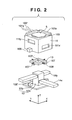
- Fig. 2 is a view showing in detail the stage (the ⁇ Z tilt stage 11 and center slider 12) used in the electron beam exposure apparatus of Fig. 1.
- the ⁇ Z tilt stage 11 comprises a substrate holder 105 which holds, e.g., the wafer 5 on its surface and reflection mirrors 101x and 101y for position measurement.
- the ⁇ Z tilt stage 11 has a cage structure surrounding the center slider 12 and has apertures 111x and 111y, through which an X movable guide 14x and a Y movable guide 14y extend.
- the position of the ⁇ Z tilt stage 11 in the X and Y directions is measured by, e.g., a laser interferometer 102 held by a sample chamber 100 shown in Fig. 1, with reference to the inner wall of the sample chamber 100.
- the ⁇ Z tilt stage 11 is also measured in the ⁇ and tilt directions.
- ⁇ measurement 102' is preferably performed from a side perpendicular to the array of a plurality of beams.
- the position in the Z-axis direction is detected by an optical sensor with non-photosensitive light.
- a vacuum encoder may be employed.
- the center slider 12 can move in the X and Y directions on the X-Y plane, which is perpendicular to the direction (substantially parallel to the Z-axis) of optical axis and parallel to the stage base 15.
- an X-Y transfer stage as shown in Fig. 4 can also be used.
- the center slider 12 will be described in detail with reference to Fig. 5.
- the center slider 12 comprises a bottom plate 12b and side plates 12s. Below the bottom plate 12b, bearings are arranged on the stage base 15 to face each other. Inside the side plates 12s, the X movable guide 14x and Y movable guide 14y are sandwiched between bearings.
- a ⁇ linear motor movable element 106 which constitutes a part of an electromagnetic actuator and a ⁇ linear motor stator 106' which constitutes the remainder of the electromagnetic actuator are provided between the ⁇ Z tilt stage 11 and the center slider 12.
- the ⁇ linear motor movable element 106 and ⁇ linear motor stator 106' drive the ⁇ Z tilt stage 11 in at least the rotation direction about the Z-axis with respect to the center slider 12. More specifically, the ⁇ linear motor movable element 106 is fixed at the end of the ⁇ Z tilt stage 11, and the ⁇ linear motor stator 106' is fixed on the bottom plate 12b of the transfer stage 12 to face the ⁇ linear motor movable element 106.
- the substrate stage can be driven in a non-contact manner.
- the ⁇ linear motor movable element 106 comprises a magnet
- the ⁇ linear motor stator 106' comprises a coil.
- the 0 linear motor movable element 106 and ⁇ linear motor stator 106' are preferably coated with multiple electromagnetic shields.
- a magnet serving as the ⁇ linear motor movable element 106 is preferably coated with multiple electromagnetic shields of, e.g., permalloy to avoid any variation in magnetic field.
- the magnet serving as the ⁇ linear motor movable element 106 is preferably spaced apart from the reduction electron optical system 4 by a sufficient distance to avoid any variation in magnetic field due to a leakage magnetic field from the reduction electron optical system 4.
- the ⁇ linear motor movable element 106 and the wafer 5 are desirably located on the opposite sides of the barycenter of the center slider 12 in the Z-axis direction.
- the ⁇ linear motor stator 106' may be arranged on the tilt frame 13.
- the center slider 12 has the X movable guide 14x and Y movable guide 14y arranged in the shape of a cross.
- the center slider 12 moves smoothly along the side surface of the Y movable guide 14y and the upper surface of the stage base 15 in the X-axis direction by moving the X movable guide 14x in the X-axis direction and moves smoothly along the side surface of the X movable guide 14x and the upper surface of the stage base 15 in the Y-axis direction by moving the Y movable guide 14y in the Y-axis direction.
- the tilt frame 13 is supported through Z actuators 107 for driving the ⁇ Z tilt stage 11 above the bottom plate 12b of the center slider 12 in the Z direction.
- the tilt frame 13 has ⁇ free leaf springs 108, each serving as a connecting member with a degree of freedom in only the ⁇ direction (rotation direction about the Z-axis).
- the ⁇ Z tilt stage 11 is supported by the tilt frame 13 through the ⁇ free leaf springs 108. Some of the ⁇ free leaf springs 108 are arranged in the X-axis direction, and the others, in the Y-axis direction.
- the ⁇ Z tilt stage 11 is rigid with respect to the tilt frame 13 in the Z-axis direction.
- the tilt frame 13 is arranged to surround the center slider 12.
- the electromagnetic actuator is provided between the substrate stage and the transfer stage.
- the substrate stage can be driven in a non-contact manner in at least the rotation direction about the Z-axis, thus preventing vibrations from being transmitted from the transfer stage to the substrate stage.
- stages (the substrate stage and transfer stage) having high-frequency band control characteristics with respect to the rotation direction about the Z-axis can be implemented. Consequently, in an electron beam exposure apparatus having these stages, especially in an electron beam exposure apparatus using a plurality of electron beams, a degradation in drawing accuracy caused by a yawing component generated in stage scanning can be reduced, and high-accuracy exposure can be realized.
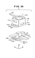
- Figs. 3A and 3B are views showing an electron beam exposure apparatus according to the second embodiment of the present invention.
- a plurality of electromagnetic actuators are combined.
- a ⁇ Z tilt stage 11 can be driven with six degrees of freedom.
- the ⁇ Z tilt stage 11 has a cage structure surrounding a center slider 12 and has apertures 111x and 111y, through which an X movable guide 14x and a Y movable guide 14y extend.
- Six linear motor movable elements 120x, 120y, and 120z, which constitute parts of respective electromagnetic actuators, are fixed on the side surface of the ⁇ Z tilt stage 11.
- Linear motor stators 120x', 120y', and 120z' which constitute the remainders of the respective electromagnetic actuators, are fixed on a bottom plate 12b to face the linear motor movable elements 120x, 120y, and 120z, respectively.
- the driving directions of the respective linear motors as electromagnetic actuators are determined by the three linear motor movable elements 120z, which generate a driving force in the Z-axis direction, the two linear motor movable elements 120x, which generate a driving force in the X-axis and ⁇ (rotation direction about the Z-axis) directions, and one linear motor movable element 120y, which generates a driving force in the Y-axis direction.
- An electromagnetic actuator which generates a driving force in the rotation direction about the X-axis and one which generates a driving force in the rotation direction about the Y-axis may also be provided in the same manner.
- the ⁇ Z tilt stage 11 can be driven with six degrees of freedom.
- a method of combining linear motors, however, is not limited to this.
- each linear motor movable element comprise a magnet
- each linear motor stator comprise a coil.
- Each electromagnetic actuator is preferably coated with multiple electromagnetic shields.
- a magnet serving as the linear motor movable element is preferably coated with multiple electromagnetic shields of, e.g., permalloy to avoid any variation in magnetic field.
- the magnet serving as the linear motor movable element is preferably spaced apart from a reduction electron optical system 4 by a sufficient distance to avoid any variation in magnetic field due to a leakage magnetic field from the reduction electron optical system 4. More specifically, each linear motor movable element and the wafer 5 are desirably located on the opposite sides of the barycenter of the center slider 12 in the Z-axis direction.
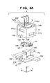
- Figs. 4A and 4B are views showing an electron beam exposure apparatus according to the third embodiment of the present invention.
- the Y-axis direction in this embodiment is a direction perpendicular to the array direction of a plurality of electron beams (B1, B2, B3,.).
- the ⁇ measurement 102' is preferably performed in a direction perpendicular to the array direction of the plurality of beams.
- a tilt frame 13 is supported on a bottom plate 12b of a center slider 12 through Z actuators 107 for driving a ⁇ Z tilt stage 11 in the Z direction.
- the tilt frame 13 is arranged to surround the center slider 12.
- piezoelectric devices with guides which are rigid in the X-Y plane may be used.
- the ⁇ Z tilt stage 11 is supported on the tilt frame 13 through ⁇ free leaf springs 108 serving as a connecting member with a degree of freedom in only the ⁇ direction (rotation direction about the Z-axis).
- the ⁇ free leaf springs 108 are arranged in the X-axis direction, and the others, in the Y-axis direction.
- the ⁇ Z tilt stage 11 is rigid with respect to the tilt frame 13 in the Z-axis direction.
- the ⁇ Z tilt stage 11 has a cage structure surrounding the center slider 12 and has apertures 111x and 111y, through which an X movable guide 14x and a Y movable guide 14y extend.
- a ⁇ linear motor movable element 106 which constitutes a part of an electromagnetic actuator is fixed on the side surface of the ⁇ Z, tilt stage 11.
- a ⁇ linear motor stator 106' which constitutes the remainder of the electromagnetic actuator is fixed on the bottom plate 12b to face the ⁇ linear motor movable element 106. Since the ⁇ linear motor movable element 106 and ⁇ linear motor stator 106' are in non-contact to each other, the substrate stage can be driven in a non-contact manner. It is thermally preferable that the ⁇ linear motor movable element 106 comprise a magnet, and the ⁇ linear motor stator 106' comprise a coil.
- the ⁇ linear motor movable element 106 and ⁇ linear motor stator 106' are preferably coated with multiple electromagnetic shields.
- a magnet serving as the ⁇ linear motor movable element 106 is preferably coated with multiple electromagnetic shields of, e.g., permalloy to avoid any variation in magnetic field.
- the magnet serving as the ⁇ linear motor movable element 106 is preferably spaced apart from a reduction electron optical system 4 by a sufficient distance to avoid any variation in magnetic field due to a leakage magnetic field from the reduction electron optical system 4.
- the ⁇ linear motor movable element 106 and the substrate are desirably located on the opposite sides of the barycenter of the center slider 12 in the Z-axis direction.
- the ⁇ linear motor stator 106' may be arranged on the tilt frame 13.
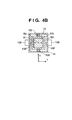
- the tilt frame 13 comprises electromagnets 130 as electromagnetic actuators which are actuated in only the Y-axis direction, as shown in Fig. 4B.
- electromagnets 130 as electromagnetic actuators which are actuated in only the Y-axis direction, as shown in Fig. 4B.
- Each electromagnet 130 is preferably coated with multiple electromagnetic shields of, e.g., permalloy to avoid any variation in magnetic field.
- the electromagnet 130 is preferably spaced apart from the reduction electron optical system 4 by a sufficient distance to avoid any variation in magnetic field due to a leakage magnetic field from the reduction electron optical system 4.
- Fig. 8 shows the flow of the whole manufacturing process of the semiconductor device.
- circuit design a semiconductor device circuit is designed.
- mask formation a mask having the designed circuit pattern is formed.
- step 3 wafer manufacture
- step 4 wafer process
- an actual circuit is formed on the wafer by lithography using the prepared mask and wafer.
- Step 5 (assembly) called a post-process is the step of forming a semiconductor chip by using the wafer formed in step 4, and includes an assembly process (dicing and bonding) and packaging process (chip encapsulation).
- step 6 the semiconductor device manufactured in step 5 undergoes inspections such as an operation confirmation test and durability test. After these steps, the semiconductor device is completed and shipped (step 7).
- Fig. 9 shows the detailed flow of the above-mentioned wafer process.
- step 11 oxidation
- step 12 CVD
- step 13 electrode formation
- step 14 ion implantation
- step 14 ion implantation
- step 15 resist processing
- step 16 exposure
- step 18 etching
- step 18 etching
- step 19 resist removal
- the present invention can provide an electron beam exposure apparatus capable of, e.g., reducing a degradation in drawing accuracy and performing high-accuracy exposure.
Landscapes
- Chemical & Material Sciences (AREA)
- Engineering & Computer Science (AREA)
- Nanotechnology (AREA)
- Analytical Chemistry (AREA)
- Crystallography & Structural Chemistry (AREA)
- Physics & Mathematics (AREA)
- General Physics & Mathematics (AREA)
- Manufacturing & Machinery (AREA)
- Mathematical Physics (AREA)
- Theoretical Computer Science (AREA)
- Condensed Matter Physics & Semiconductors (AREA)
- Exposure And Positioning Against Photoresist Photosensitive Materials (AREA)
- Electron Beam Exposure (AREA)
Applications Claiming Priority (2)
| Application Number | Priority Date | Filing Date | Title |
|---|---|---|---|
| JP2002210159A JP2004055767A (ja) | 2002-07-18 | 2002-07-18 | 電子ビーム露光装置及び半導体デバイスの製造方法 |
| JP2002210159 | 2002-07-18 |
Publications (2)
| Publication Number | Publication Date |
|---|---|
| EP1383157A2 true EP1383157A2 (de) | 2004-01-21 |
| EP1383157A3 EP1383157A3 (de) | 2005-11-23 |
Family
ID=29774662
Family Applications (1)
| Application Number | Title | Priority Date | Filing Date |
|---|---|---|---|
| EP03254452A Withdrawn EP1383157A3 (de) | 2002-07-18 | 2003-07-15 | Elektronenstrahlbelichtungsverfahren und Verfahren zur Herstellung einer Halbleitervorrichtung |
Country Status (3)
| Country | Link |
|---|---|
| US (1) | US6930756B2 (de) |
| EP (1) | EP1383157A3 (de) |
| JP (1) | JP2004055767A (de) |
Cited By (3)
| Publication number | Priority date | Publication date | Assignee | Title |
|---|---|---|---|---|
| WO2010021543A1 (en) * | 2008-08-18 | 2010-02-25 | Mapper Lithography Ip B.V. | Charged particle beam lithography system and target positioning device |
| NL2001896C (en) * | 2008-08-18 | 2010-03-10 | Mapper Lithography Ip Bv | Charged particle beam lithography system and target positioning device. |
| US8779392B2 (en) | 2008-08-18 | 2014-07-15 | Mapper Lithography Ip B.V. | Charged particle beam lithography system and target positioning device |
Families Citing this family (16)
| Publication number | Priority date | Publication date | Assignee | Title |
|---|---|---|---|---|
| JP2005005393A (ja) * | 2003-06-10 | 2005-01-06 | Canon Inc | ステージ装置、露光装置、およびデバイス製造方法 |
| JP2005005394A (ja) * | 2003-06-10 | 2005-01-06 | Canon Inc | ステージ装置、露光装置、およびデバイス製造方法 |
| JP2010519697A (ja) * | 2007-02-22 | 2010-06-03 | アプライド マテリアルズ イスラエル リミテッド | 高スループットsemツール |
| JP2010084207A (ja) * | 2008-09-30 | 2010-04-15 | Canon Anelva Corp | 処理装置及び画像表示装置 |
| JP2010084205A (ja) * | 2008-09-30 | 2010-04-15 | Canon Anelva Corp | 保持機構、当該保持機構を備えた処理装置、処理装置を用いた成膜方法及び画像表示装置の製造方法 |
| EP2382243A1 (de) * | 2009-01-29 | 2011-11-02 | ExxonMobil Chemical Patents Inc. | Polypropylenvliesfasern und -stoffe, und verfahren zu deren herstellung |
| WO2011007433A1 (ja) * | 2009-07-15 | 2011-01-20 | パイオニア株式会社 | 撮像装置 |
| US20120145885A1 (en) * | 2009-07-15 | 2012-06-14 | Pioneer Corporation | Imaging apparatus |
| TW201337469A (zh) | 2011-09-12 | 2013-09-16 | 瑪波微影Ip公司 | 具有基底板之真空腔室 |
| JP6262024B2 (ja) | 2014-03-04 | 2018-01-17 | 株式会社ニューフレアテクノロジー | マルチ荷電粒子ビーム描画装置 |
| JP2016207756A (ja) * | 2015-04-17 | 2016-12-08 | 株式会社ニコン | ステージ装置及び露光装置 |
| EP3488245B1 (de) * | 2016-07-21 | 2022-10-12 | Siemens Healthcare Diagnostics Inc. | Konstruktion eines linearmotorgehäuses |
| WO2019211123A1 (en) | 2018-05-02 | 2019-11-07 | Asml Netherlands B.V. | E-beam apparatus |
| KR20240095476A (ko) * | 2019-05-31 | 2024-06-25 | 에이에스엠엘 네델란즈 비.브이. | 다중 하전 입자 빔 장치 및 그 작동 방법 |
| JP7360978B2 (ja) * | 2020-03-18 | 2023-10-13 | 株式会社日立ハイテクサイエンス | 荷電粒子ビーム装置 |
| DE102024117811A1 (de) * | 2024-06-25 | 2026-01-08 | Physik Instrumente (PI) SE & Co KG | Verstellvorrichtung, Verwendung einer solchen Verstellvorrichtung zur Positionierung von Gegenständen und Verfahren zur Positionierung von Gegenständen unter Verwendung einer solchen Verstellvorrichtung |
Citations (4)
| Publication number | Priority date | Publication date | Assignee | Title |
|---|---|---|---|---|
| JPH03155113A (ja) * | 1989-11-14 | 1991-07-03 | Canon Inc | 露光装置 |
| EP0794552A2 (de) | 1996-03-04 | 1997-09-10 | Canon Kabushiki Kaisha | Elektronenstrahl-Belichtungsgerät, Belichtungsverfahren und Verfahren zur Erzeugung eines Objekts |
| US20010025932A1 (en) | 2000-04-03 | 2001-10-04 | Nikon Corporation | Charged-particle-beam microlithography apparatus and methods including shielding of the beam from extraneous magnetic fields |
| US6337484B1 (en) | 1998-07-17 | 2002-01-08 | Asm Lithography, B.V. | Positioning device and lithographic projection apparatus comprising such a device |
Family Cites Families (7)
| Publication number | Priority date | Publication date | Assignee | Title |
|---|---|---|---|---|
| JPH0589815A (ja) | 1991-09-26 | 1993-04-09 | Hitachi Ltd | 電子線応用装置 |
| JP2974535B2 (ja) * | 1993-03-11 | 1999-11-10 | キヤノン株式会社 | 位置決め装置 |
| JP3164960B2 (ja) * | 1994-02-18 | 2001-05-14 | キヤノン株式会社 | ステージ装置 |
| JPH08229759A (ja) | 1995-02-24 | 1996-09-10 | Canon Inc | 位置決め装置並びにデバイス製造装置及び方法 |
| JP3927620B2 (ja) | 1996-06-12 | 2007-06-13 | キヤノン株式会社 | 電子ビーム露光方法及びそれを用いたデバイス製造方法 |
| JP3689516B2 (ja) | 1997-01-29 | 2005-08-31 | キヤノン株式会社 | 電子ビーム露光装置 |
| JP2000049071A (ja) * | 1998-07-28 | 2000-02-18 | Canon Inc | 電子ビーム露光装置及び方法、ならびにデバイス製造方法 |
-
2002
- 2002-07-18 JP JP2002210159A patent/JP2004055767A/ja active Pending
-
2003
- 2003-07-14 US US10/617,682 patent/US6930756B2/en not_active Expired - Fee Related
- 2003-07-15 EP EP03254452A patent/EP1383157A3/de not_active Withdrawn
Patent Citations (4)
| Publication number | Priority date | Publication date | Assignee | Title |
|---|---|---|---|---|
| JPH03155113A (ja) * | 1989-11-14 | 1991-07-03 | Canon Inc | 露光装置 |
| EP0794552A2 (de) | 1996-03-04 | 1997-09-10 | Canon Kabushiki Kaisha | Elektronenstrahl-Belichtungsgerät, Belichtungsverfahren und Verfahren zur Erzeugung eines Objekts |
| US6337484B1 (en) | 1998-07-17 | 2002-01-08 | Asm Lithography, B.V. | Positioning device and lithographic projection apparatus comprising such a device |
| US20010025932A1 (en) | 2000-04-03 | 2001-10-04 | Nikon Corporation | Charged-particle-beam microlithography apparatus and methods including shielding of the beam from extraneous magnetic fields |
Cited By (8)
| Publication number | Priority date | Publication date | Assignee | Title |
|---|---|---|---|---|
| WO2010021543A1 (en) * | 2008-08-18 | 2010-02-25 | Mapper Lithography Ip B.V. | Charged particle beam lithography system and target positioning device |
| NL2001896C (en) * | 2008-08-18 | 2010-03-10 | Mapper Lithography Ip Bv | Charged particle beam lithography system and target positioning device. |
| CN102187424A (zh) * | 2008-08-18 | 2011-09-14 | 迈普尔平版印刷Ip有限公司 | 带电粒子束光刻系统以及目标定位装置 |
| CN102187424B (zh) * | 2008-08-18 | 2013-07-17 | 迈普尔平版印刷Ip有限公司 | 带电粒子束光刻系统以及目标定位装置 |
| US8779392B2 (en) | 2008-08-18 | 2014-07-15 | Mapper Lithography Ip B.V. | Charged particle beam lithography system and target positioning device |
| US8796644B2 (en) | 2008-08-18 | 2014-08-05 | Mapper Lithography Ip B.V. | Charged particle beam lithography system and target positioning device |
| US8957395B2 (en) | 2008-08-18 | 2015-02-17 | Mapper Lithography Ip B.V. | Charged particle beam lithography system and target positioning device |
| US9082584B2 (en) | 2008-08-18 | 2015-07-14 | Mapper Lithography Ip B.V. | Charged particle beam lithography system and target positioning device |
Also Published As
| Publication number | Publication date |
|---|---|
| JP2004055767A (ja) | 2004-02-19 |
| EP1383157A3 (de) | 2005-11-23 |
| US6930756B2 (en) | 2005-08-16 |
| US20040012765A1 (en) | 2004-01-22 |
Similar Documents
| Publication | Publication Date | Title |
|---|---|---|
| US6930756B2 (en) | Electron beam exposure apparatus and semiconductor device manufacturing method | |
| US7057193B2 (en) | Exposure apparatus | |
| US7005658B2 (en) | Charged particle beam exposure apparatus and method | |
| US6784442B2 (en) | Exposure apparatus, control method thereof, and device manufacturing method | |
| EP1253619A2 (de) | Ladungsträgerteilchenstrahl-Belichtungsgerät und dessen Anwendungverfahren zur Herstellung von Vorrichtungen | |
| US7795597B2 (en) | Deflector array, exposure apparatus, and device manufacturing method | |
| JPH09330871A (ja) | 電子ビーム露光システム及びそれを用いたデバイス製造方法 | |
| US7030964B2 (en) | Stage system, exposure apparatus, and device manufacturing method | |
| JP2006210503A (ja) | 収差調整方法、デバイス製造方法及び荷電粒子線露光装置 | |
| EP1398109B1 (de) | Trägervorrichtung und Antriebsverfahren, Belichtungsapparat und Herstellungsverfahren | |
| US6989888B2 (en) | Stage system, exposure apparatus, and device manufacturing method | |
| US11276558B2 (en) | Exposure apparatus and exposure method, lithography method, and device manufacturing method | |
| JP5159035B2 (ja) | レンズアレイ及び該レンズアレイを含む荷電粒子線露光装置 | |
| JP3647143B2 (ja) | 電子ビーム露光装置及びその露光方法 | |
| JP2000133565A (ja) | 荷電粒子線露光方法及び装置、ならびにデバイス製造方法 | |
| JP4143204B2 (ja) | 荷電粒子線露光装置及び該装置を用いたデバイス製造方法 | |
| JP3919255B2 (ja) | 電子ビーム露光装置及びデバイス製造方法 | |
| JP2005209709A (ja) | ステージ装置 | |
| JP4559137B2 (ja) | 真空機器の製造装置及び製造方法 | |
| JP4913521B2 (ja) | 荷電粒子線装置及びデバイス製造方法 | |
| JP4006054B2 (ja) | 電子ビーム露光装置 | |
| JP2000150354A (ja) | 荷電粒子線露光方法及び装置、ならびにデバイス製造方法 |
Legal Events
| Date | Code | Title | Description |
|---|---|---|---|
| PUAI | Public reference made under article 153(3) epc to a published international application that has entered the european phase |
Free format text: ORIGINAL CODE: 0009012 |
|
| AK | Designated contracting states |
Kind code of ref document: A2 Designated state(s): AT BE BG CH CY CZ DE DK EE ES FI FR GB GR HU IE IT LI LU MC NL PT RO SE SI SK TR |
|
| AX | Request for extension of the european patent |
Extension state: AL LT LV MK |
|
| PUAL | Search report despatched |
Free format text: ORIGINAL CODE: 0009013 |
|
| AK | Designated contracting states |
Kind code of ref document: A3 Designated state(s): AT BE BG CH CY CZ DE DK EE ES FI FR GB GR HU IE IT LI LU MC NL PT RO SE SI SK TR |
|
| AX | Request for extension of the european patent |
Extension state: AL LT LV MK |
|
| RIC1 | Information provided on ipc code assigned before grant |
Ipc: 7H 01J 37/20 B Ipc: 7H 01L 21/00 B Ipc: 7H 01J 37/317 B Ipc: 7H 01J 37/30 A |
|
| 17P | Request for examination filed |
Effective date: 20060523 |
|
| AKX | Designation fees paid |
Designated state(s): DE FR GB IT NL |
|
| 17Q | First examination report despatched |
Effective date: 20060801 |
|
| STAA | Information on the status of an ep patent application or granted ep patent |
Free format text: STATUS: THE APPLICATION HAS BEEN WITHDRAWN |
|
| 18W | Application withdrawn |
Effective date: 20150219 |