EP1385193B9 - Lentille d'objectif pour système de microscopie électronique, et système de microscopie électronique - Google Patents
Lentille d'objectif pour système de microscopie électronique, et système de microscopie électronique Download PDFInfo
- Publication number
- EP1385193B9 EP1385193B9 EP03016238A EP03016238A EP1385193B9 EP 1385193 B9 EP1385193 B9 EP 1385193B9 EP 03016238 A EP03016238 A EP 03016238A EP 03016238 A EP03016238 A EP 03016238A EP 1385193 B9 EP1385193 B9 EP 1385193B9
- Authority
- EP
- European Patent Office
- Prior art keywords
- objective lens
- pole shoe
- pole piece
- outer pole
- terminal electrode
- Prior art date
- Legal status (The legal status is an assumption and is not a legal conclusion. Google has not performed a legal analysis and makes no representation as to the accuracy of the status listed.)
- Expired - Lifetime
Links
Images



Classifications
-
- H—ELECTRICITY
- H01—ELECTRIC ELEMENTS
- H01J—ELECTRIC DISCHARGE TUBES OR DISCHARGE LAMPS
- H01J37/00—Discharge tubes with provision for introducing objects or material to be exposed to the discharge, e.g. for the purpose of examination or processing thereof
- H01J37/02—Details
- H01J37/04—Arrangements of electrodes and associated parts for generating or controlling the discharge, e.g. electron-optical arrangement or ion-optical arrangement
- H01J37/10—Lenses
- H01J37/145—Combinations of electrostatic and magnetic lenses
-
- H—ELECTRICITY
- H01—ELECTRIC ELEMENTS
- H01J—ELECTRIC DISCHARGE TUBES OR DISCHARGE LAMPS
- H01J2237/00—Discharge tubes exposing object to beam, e.g. for analysis treatment, etching, imaging
- H01J2237/26—Electron or ion microscopes
- H01J2237/28—Scanning microscopes
- H01J2237/2813—Scanning microscopes characterised by the application
- H01J2237/2817—Pattern inspection
-
- H—ELECTRICITY
- H01—ELECTRIC ELEMENTS
- H01J—ELECTRIC DISCHARGE TUBES OR DISCHARGE LAMPS
- H01J2237/00—Discharge tubes exposing object to beam, e.g. for analysis treatment, etching, imaging
- H01J2237/30—Electron or ion beam tubes for processing objects
- H01J2237/317—Processing objects on a microscale
- H01J2237/3174—Etching microareas
- H01J2237/31745—Etching microareas for preparing specimen to be viewed in microscopes or analyzed in microanalysers
-
- H—ELECTRICITY
- H01—ELECTRIC ELEMENTS
- H01J—ELECTRIC DISCHARGE TUBES OR DISCHARGE LAMPS
- H01J2237/00—Discharge tubes exposing object to beam, e.g. for analysis treatment, etching, imaging
- H01J2237/30—Electron or ion beam tubes for processing objects
- H01J2237/317—Processing objects on a microscale
- H01J2237/31749—Focused ion beam
Definitions
- the invention relates to an electron microscopy system with magnetic and electrostatic focusing, and more particularly to an objective lens for such a system. Further, the invention relates to an inspection system for imaging and manipulating an object comprising such an electron microscopy system.
- a technique is to "mill" a trench in the structure to be characterized in order to examine a cross section through the structure and so with relatively little Workload to be able to receive a wealth of information, eg regarding the sequence of layers in the structure.
- Such a trench is etched into the semiconductor structure, for example with the aid of a focused ion beam (FIB).
- FIB focused ion beam
- This etching method is of particular importance for the production of sample cross-sections for transmission electron microscopy or in the case of a structure having a complex layer sequence and different etching selectivity of the individual layers.
- Methods using a FIB allow for the production of quite fine and well-defined cuts. It is advantageous in this method to observe the etching process in situ microscopically.
- Such an objective lens which has proved to be advantageous, provides a combination of magnetic and electrostatic focusing or delay.
- FIG. 1 An example of a conventional objective lens is shown in FIG FIG. 1 shown schematically.
- the objective lens 1 comprises a rotationally symmetrical about an optical axis 2 of the objective lens arranged magnetic lens with a Polschuhan extract with an inner pole piece 11 and an outer pole piece 12 and with a arranged in a space between the inner and outer pole piece 11, 12 bobbin 15.
- the The objective lens 1 is an electrostatic immersion lens having a beam tube 13 forming a first electrode and a termination electrode 14.
- the beam tube 13 is disposed substantially in a lower portion of an inner space formed by the inner pole piece 11, while the termination electrode 14 is spatially substantially in the z direction connects to the outer pole piece.
- the pole shoe material carries a large part of the river.
- Magnetic field strength and extension of the magnetic field on the optical axis 2 are of importance for the focal length.
- the focal length is proportional to the acceleration voltage of the electrons divided by the spatial integral over the square of the magnetic flux density in the region of the pole pieces along the z-axis.
- a positive voltage is applied, while the termination electrode 14 is preferably connected to ground potential.
- the electrostatic lens generates a retarding field in which the electrons of the electron beam are decelerated before leaving the electron optics. This allows the electrons of the electron beam to pass through most of the beam path between the electron source and the electrostatic lens at high energy and speed, thus minimizing the negative impact electrostatic repulsion phenomena of the like charged electrons.
- the electrostatic field between the end of the tube and the end electrode 14 also has an inhomogeneity such that this field also acts focusing on the primary electrons passing through it.
- An electron microscope device comprising such an objective lens has also been advantageously employed in an arrangement for imaging and manipulating an object additionally comprising an apparatus for generating and controlling a focused ion beam (hereinafter also referred to as an ion beam processing system or FIB pillar).
- an arrangement for mapping and editing of the structure to be carried out simultaneously Due to the space requirement of the above-described objective lens of the electron-optical arrangement and the FIB column, a surface-extended object to be examined can be arranged with simultaneous imaging and processing at a maximum angle of 80 ° relative to the ion beam.
- a surface-extended object to be examined can be arranged with simultaneous imaging and processing at a maximum angle of 80 ° relative to the ion beam.
- vertical-wall trenches in an object can not be generated simultaneously with the electron microscope. Rather, after an operation to process the object by the FIB, the object is tilted and rotated, and then the structure produced by the FIB is mapped.
- a magnetic field in the region of the object manipulated by the ion beam is to be minimized because the ions are deflected by the magnetic field, resulting in deterioration of the machining precision of the focused ion beam. Furthermore, in such a magnetic field, a splitting of the ion beam into isotopes may occur, which possibly completely precludes its usability.
- the objective lens further comprises a bobbin disposed in a space between the inner and outer pole pieces.
- the geometry and arrangement of the components of the conventional objective lens have been changed to accommodate a first aspect so as to be able to reduce the angle between the conical outer pole piece and the z-axis and thus to reduce the space requirement of the objective lens and thus electron microscopic arrangement.
- a substantially flat-extended object can be more tilted with respect to the optical axis of the electron microscope arrangement.
- the working distance is to be understood here as the distance between a lowermost region or a lower end of the terminating electrode and the object plane or an object arranged in the latter, whereby a resolution-best imaging can be achieved or a resolution can be achieved at this working distance when used as intended which is not significantly different from the specified resolution when used as intended.
- the objective lens can be advantageously used even when using larger working distances.
- the latter At a lowest point in the z-direction of the inner pole piece, the latter has a gap distance oriented in the z-direction from the outer pole piece, where a pole shoe gap is formed between the inner and outer pole piece.
- the magnetic field exits in the direction of the optical axis.
- the dimensions of the Polschuhspalts have an influence on the strength as well as the spatial extent of the magnetic field on the optical axis and thus on the focal length of the objective lens.
- the characteristics of spherical and chromatic aberration must be balanced against the focusing power that is reduced by the field flattening due to material saturation or too large a gap width.
- a Polschuhspaltabstand of at least 3 mm When specifying this distance, it should be noted that this is effectively an effective Polschuhspaltabstand. That means, that it is possible, by adding additional material in the form of, for example, a thin extension or thin films or foils, to reduce the pole shoe gap or pole shoe spacing under a geometrical but not under a functional aspect. Because of this added material, the magnetic field generated by the magnetic lens, and thus the magnetic flux lines emanating from the inner and outer pole pieces, are not significantly affected by magnetic saturation in the added material, or the material is added at a point where there is hardly any flow at all located in the pole piece.
- an inner and an outer side of the inner pole piece extend upward from a lowest point of the inner pole piece in the z-direction in a conical shape.
- the inner pole piece is designed such that it extends from its lower end in the form of a cylinder jacket about 1 mm to 3 mm in the z-direction upwards, before it widens conically at least on an outer side.
- the outer pole piece tapers downwards.
- the inner pole piece at least at its lower end an inner diameter of 6 mm to 8 mm, with an inner diameter of 7.5 mm is particularly preferred.
- the dimension of the radially innermost axially lowermost portion of the outer pole piece located axially about the axis is preferably in a range of 0.5 mm to 3 mm, the dimension of the radially innermost axially axially disposed lowest portion of the inner pole piece is preferably 10 mm and more.
- a lower end of the terminal electrode in the z-direction is spaced from a z-direction lowermost region of the outer pole piece in the z-direction.
- the jet pipe is arranged such that it at least passes through an opening of the outer pole shoe formed by a region of the outer pole shoe that is the lowest in the z direction.
- the jet pipe passes through the opening of the outer pole piece and the lower end of the steel tube is arranged so that it is spaced in the z-direction from the opening of the outer pole piece, ie parallel to the optical axis extending from the pole piece, in particular the opening of the outer pole piece emerges.
- the lower end of the jet pipe in the z-direction is particularly preferred between the opening of the outer pole piece and the lower end of the termination electrode.
- an objective lens in addition to the above-described particular geometric configuration of the magnetic lens formed by the pole piece assembly (including the preferred embodiments), is characterized by a magnetic coupling of the outer pole piece and the termination electrode.
- This magnetic coupling is achieved in that the outer pole piece, which is bounded outwardly substantially by a conical surface with a cone angle ( ⁇ ) to the z-direction, and the terminal electrode, which outwardly substantially by a conical surface with a cone angle ( ⁇ ') is limited to the z-direction, are coupled to reduce the magnetic field on the object plane in the object object substantially gap-free magnetically with each other.
- This magnetic coupling causes a better shielding of the magnetic field to areas outside the objective lens, which is particularly advantageous in cases where the magnetic field interferes with the object or a sample or in the simultaneous processing of the examined object by means of a focused ion beam, because the magnetic field would distract the ions and thus interfere with the machining process.
- the objective lens is also designed under this aspect so that a working distance is less than 2 mm for electrons that pass through the beam pipe at about 30 keV.
- the magnetic coupling between the termination electrode and the outer pole piece is achieved in that a gap between the termination electrode and the outer pole piece is smaller than 0.6 mm and even more preferably less than 0.2 mm.
- a gap between the terminal electrode and the outer pole piece is advantageously formed in that a region of the terminal electrode and a region of the outer pole piece face each other in a planar manner.
- an uppermost region of the terminal electrode in the z-direction and the region of the outer pole shoe which is the lowest in the z-direction lie flat, wherein preferably the opposing surfaces are arranged parallel to the z-direction, and more preferably at least that of the outer pole shoe opposite region of the terminal electrode is disposed within the opening formed by the z-direction in the lowest area of the outer pole piece opening.
- the terminating electrode is held by a plastic insulation extending from a lower region of the outer pole shoe along the inside of the inner pole shoe and electrically insulated clamps.
- a plastic insulation extending from a lower region of the outer pole shoe along the inside of the inner pole shoe and electrically insulated clamps.
- outer pole piece and termination electrode in which the at least partially substantially conically extending outer sides of the outer pole piece and the termination electrode are aligned with one another.
- the termination electrode is advantageously designed so that they are up to a central opening at the lower end of the End electrode tapers substantially conically and so the electrostatic field is provided comparatively close to an object or a sample.
- the termination electrode is preferably connected to ground potential, the electrostatic field is negligibly small in a region of the sample.
- the proximity of the field to the sample is particularly advantageous for larger working distances W D , ie distances between the terminal electrode and the sample surface.
- the inner diameter of the central opening of the termination electrode substantially corresponds to an inner diameter of the jet pipe, but embodiments are also provided in which the central opening at the lower end of the termination electrode has a different inner diameter than the inner diameter of the jet pipe.
- the electrostatic lens of the objective lens in addition to the above-described special geometric parameters of the magnetic lens and / or magnetic coupling of outer pole piece and terminal electrode including the described in connection with these preferred embodiments, designed such that a distance A 1 between the lower end of the inner pole piece and the lower end and the lowest point in the z-direction of the jet pipe is greater than 9 mm and more preferably greater than 10 mm.
- This embodiment is particularly preferably provided for reducing the magnetic field in the object plane.
- the lower end of the jet pipe is arranged in the z-direction between the lowermost region of the outer pole piece and the lower end of the termination electrode.
- a distance A 2 between the lower end of the jet pipe and the lower End of the termination electrode greater than 3 mm, more preferably a distance of about 6 mm.
- This arrangement is based on the idea to reduce an overlap of the magnetic field generated by the magnetic lens and the electrostatic field generated by the terminal electrode and beam tube electrostatic field with respect to the known from the prior art arrangement.
- the electrostatic and magnetic fields in such a lens geometry preferably overlap by less than 5% (relative to the field integrals).
- the magnetic field generated by the magnetic lens at a greater distance to an object to be imaged, whereby a magnetic field in the object plane or on the object is minimized.
- Reasons why this field minimization on the object is advantageous have already been mentioned before.
- Another advantage of this arrangement is that the electrostatic field is located close to the sample, which is particularly advantageous for larger working distances.
- the lower end of the jet pipe has an end flange which extends radially beyond an outer diameter of the jet pipe.
- the end flange enclosing the jet tube has a distance to the termination electrode, which is large enough to prevent the occurrence of electrical flashovers or short circuits.
- This end flange is preferably designed such that in the axial cross-section it merges from a front section pointing in the direction of the object plane to a jacket section in rounded form, this rounding having a radius of curvature of at least one millimeter.
- This particular embodiment of the jet pipe is based on the idea, in the area substantially between the inner pole piece and the jet pipe, made of plastic components of the objective lens before to protect a charge by an electron cloud inevitably occurring in the operation of the electron microscope assembly by, as it were, the direct access to this area is made difficult by the shielding by the end flange and the primary electron beam is shielded similar as by a Faraday cage.
- the end flange can also be designed such that a transition from the inner diameter bounding inner wall of the jet pipe is rounded to the front surface.
- a material is preferably selected for the pole shoes, which has a high saturation magnetization.
- an iron-nickel alloy is used with a nickel content of 45% to 50%.
- a NiFe alloy with the trade name "Permenorm 5000 H3", commercially available from Vacuumschmelze Hanau, Germany.
- a cobalt-iron-vanadium (49% Co-49% Fe-2% V) alloy, cobalt-iron alloys (e.g., 30% Co, 70% Fe) or soft iron may also be used.
- the material used for the bobbin preferably comprises copper wire.
- the bobbin is thermally insulated from the pole pieces, heat generated in the bobbin when current flows through a thermally coupled to the bobbin, received in the interior space between the inner and outer pole piece water cooling pipe and transported away through the cooling circuit.
- a so-called ⁇ metal ie a nickel-iron alloy with a nickel content of 72-89%, is preferably selected for the termination electrode, particularly preferably Hyperm 766.
- an electron microscopy system comprises further components: a sample chamber in which an object to be examined is arranged, an electron beam source for generating and accelerating an electron beam, electron optics with one or more electrostatic and / or magnetic lens (s), at least one vacuum system for evacuating at least the electron beam traversed by the electron beam and the sample chamber, an object holder in the sample chamber for arranging and aligning an object in front of the electron microscope and at least one detector for detecting electrons, in particular secondary electrons.
- at least one detector is provided in an inner space of the electron microscope, which is arranged in the z-direction above the objective lens.
- the ion beam processing system is provided for generating and directing a focused ion beam, by means of which an object to be examined is manipulated, for example, by removing material from a defined area of the surface of the object.
- an object to be examined is manipulated, for example, by removing material from a defined area of the surface of the object.
- repair work on lithographic masks or direct-writing lithography processes using this arrangement.
- the ion beam processing system includes an ion source for generating an ion beam, often using a liquid metal ion source (often gallium or indium) and an extraction electrode for extracting ions from the ion source by applying an electrostatic field.
- ion optics of the ion beam processing system for accelerating, focusing, and deflecting the ion beam include at least one accelerating electrode, electrostatic lenses, variable aperture, and deflecting units.
- the electron microscopy system and the ion beam processing system are arranged to each other such that their optical axes intersect substantially in a plane defined by a surface of the object to be examined.
- the object is held by an object holder which has a defined orientation of the object in front of the electron microscopy system and the ion beam processing system allowed.
- the angle at which the focused ion beam and the focused electron beam impinge on the object surface can be set in a defined angular range.
- the ion beam can be arranged perpendicular to the object and therefore enables the creation of trenches with vertical side walls, which are of great importance for certain fields of application.
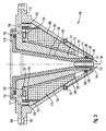
- An in Figures 3 . 4 and 5 shown objective lens 100 is used to focus an electron beam in a Elektronenmikroskopieanssen.
- the objective lens 100 comprises a magnetic lens as well as an electrostatic lens, thus the focusing is done both electrostatically and magnetically.
- the electrostatic lens also serves to decelerate the electrons of the primary electron beam.
- the magnetic lens comprises a pole piece arrangement with an inner pole piece 111 and an outer pole piece 112. Both pole pieces 111, 112 are a central optical axis 101, ie, the rotational direction of the beam path of a primary electron beam is rotationally symmetrical.
- the inner pole piece 111 has a substantially conical shape in the z direction and tapers continuously in this cone-shaped area in the direction of the object plane. In a lowermost region of the inner pole piece 111 in the z-direction, the latter has a hollow-cylindrical region 111 'extending in the z-direction over approximately 2.2 mm.
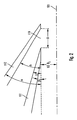
- the inner side 190 of the inner pole piece 111 extends from a lowermost position 192 in the z-direction first about 32 mm parallel to the axis 101 and then extends along a cone with an angle ⁇ of 10.5 ° to the z-axis, to this merges into a radial flange 111 '', which in its outer region is opposite a radial flange region 112 'of the outer pole shoe 112.
- the outer, further away from the axis 101 surface 191 of the inner pole piece 111 extends only in the hollow cylindrical Area 111 'about 2.2 mm parallel to the optical axis and then passes into a cone at an angle ⁇ of 16 ° to the z-axis until it merges into a Radialflanschteil 111 "of the inner pole piece 111.
- the outer pole piece 112 extends substantially conically in the z direction up to an upper flange area 112 '.
- An inner side 180 of the outer pole piece 112 in this conical region forms an angle ⁇ of 29 ° with respect to the axis 101, while an outer side 181 extends radially outward at an angle ⁇ of 34 ° to the axis 101.
- this has a central opening whose inner diameter is substantially equal to the inner diameter D i (see. FIG. 2 ) corresponds to the opening at the lowest point 192 in the inner pole piece 111 in the z-direction.
- a distance between the two pole pieces decreases in the direction of the object plane and reaches a smallest dimension in a lower region 111 'of the inner pole piece 111.
- an axial pole piece gap 119 running parallel to the z-direction and having a pole piece spacing is formed.
- the pole piece gap 119 in this embodiment has an axial length of about 6 mm.
- the arrangement and configuration of Polschuhspalts 119 is for the function of the magnetic lens of great importance.
- the pole pieces 111, 112 "somewhat" cling to the magnetic field.
- the field lines extend between the upper and the lower pole piece bulged in the direction of the optical axis 101 bulged shape.
- a maximum field strength on the optical axis 101 is in the region of the Polschuhspalts 119 reaches, wherein the field strength of the generated magnetic field substantially in the z-direction has a bell shape.
- a flat support ring 116 is disposed of non-magnetic material at the lowest end 192 of the inner pole piece 111 in Polschuhspalt 119, which has the same inner diameter as the hollow cylindrical portion 111 'of the inner pole piece 111, but a larger outer diameter.
- Polschuhspalt 119 a made of elastic material sealing ring 130 is further provided which abuts areas of the support ring 116, the outer pole piece 112 and a lower portion of insulation 118 'and a seal of the enclosed by the pole pieces 111, 112 space of the vacuum space in Area of an object to be examined and within the electron microscopy system.
- the Polschuhan extract is made of Permenorm ® 5000 H3, an iron-nickel alloy, by turning and subsequent annealing. A diagram of the field dependent flux density or magnetization of this material is in FIG. 6 played.
- a bobbin 115 is arranged in the inner space formed between the inner pole piece 111 and the outer pole piece 112.
- the bobbin 115 comprises coaxially with the optical axis arranged wire coils with a wire thickness of 0.8 mm and is made of copper. The number of turns is 650.
- the coils can be operated with a maximum current of 2A. A resulting in current flow through the coils heat output is in the range of about 20 watts.
- Between the coil turns is a Epoxy resin filled, which causes thermal and mechanical stability after curing.
- the bobbin 115 is substantially adapted in shape to the shape of the interior formed by the pole pieces 111, 112 without completely filling it.
- an upper side and an inner and an outer side of the bobbin 115 extend substantially parallel to the respective opposite surfaces of the pole piece assembly.
- the bobbin 115 is enclosed gap-free by a first jacket 120 and extends in a region of the outer side of the bobbin 115 extending parallel to the z-axis a second sheath 122 enclosed gap-free.
- the sheaths 120, 122 are made of copper and serve to absorb and dissipate heat that is generated in current passage in the wire coils of the bobbin 115.
- a gap 123 is left over the entirety of the area of the inner pole piece 111 opposite the first sheath 120 in order to provide thermal insulation and substantially prevent heating of the pole shoe material .
- an annular spacer 131 is inserted between a short vertical extension 120 'of the first shell 120 and the outer side 191 of the inner pole piece 111 to contact the pole piece 111 and the first shell 120 to prevent and provide the gap 123.
- the vertical extension of the first casing 120 is followed in the horizontal direction radially outward by a pipe 121 through which cooling water flows.
- a gap 124 for thermal insulation.
- the second sheath 122 has an essentially inverted L-shape and runs parallel to a parallel to the axis 101 portion of the outer side of the bobbin 115, while in the horizontal direction spatially connects to the first sheath 120 and a bore for receiving a screw 153, which is provided for connecting inner pole piece 111 and bobbin 115 with sheaths 120, 122 using a switching body 135. Between a head of the screw 153 and the second casing 122, a washer 132 is disposed.
- the flange portion 111 '' of the inner pole piece 111 and an opposite flange 112 'of the outer pole piece 112 have mutually aligned bores 154 and 155 for screwing the two pole pieces 111, 112 together.
- the outer pole piece 112 further has on its outer side 181 in the region of the transition from cone shape to the flange region 112 'on a step shape, which serves to fit the Polschuhan extract in a corresponding, manufactured for receiving part of the electron microscope.
- An insulation 118 made of plastic extends parallel to and along the inner side 190 of the inner pole piece 111 in a lower region beyond a lower end 192 of the inner pole piece 111 to about a lowest point 182 of the outer pole piece 112.
- In an upper area goes the insulation 118 parallel to the inner pole piece 111 in a flange portion 118 '' over, which extends approximately to the middle of the flange portion 111 '' of the inner pole piece 111.
- In an edge region of the flange portion 118 '' of the insulation 118 is a bore for receiving a the insulation 118 with the inner pole piece 111 connecting Screw 152 provided.
- annular recess for receiving a sealing ring 133 is provided in a side of the insulation 118 facing the inner pole piece 111.
- the insulation 118 In a conical portion of the inner side of the inner pole piece 111, the insulation 118 is spaced from the inner pole piece 111 leaving a gap.
- the insulation 118 assumes a hollow cylindrical shape 118 'in a lower region. In this hollow-cylindrical region 118 'of the insulation 118, this has an annular recess 117 which extends over almost the entire height of the hollow-cylindrical region and accommodates saddle-shaped deflection coils (not shown) for deflecting the electron beam.
- the jet pipe 113 forming a first electrode of the electrostatic lens is fitted.
- the jet pipe 113 extends in the z-direction beyond both an upper and a lower end of the hollow cylindrical portion 118 'of the insulation 118.
- the inner diameter of the jet pipe 113 is about 4.5 mm.
- a lower end of the beam tube 113 has a distance to the lowest point or the lower end 182 of the outer pole piece 112 of about 5 mm.
- the jet pipe 113 in this embodiment has an end flange 113 'having a rounded shape in axial cross-section and having a diameter of about 8.5 mm at its greatest radially outwardly extending extent.
- the end flange 113 ' extends from a pointing in the direction of the object plane front portion 113' in a rounded shape in a substantially parallel to the axis 101 disposed shell portion 113 ''', wherein the radius of curvature R F of this rounding is about 2 mm.
- the this bottom flange 113 'assigning the lowest part of the insulation 118 and the Shape of the end flange 113 'of the jet pipe 113 are adapted to each other so that their surfaces are arranged substantially parallel and so a gap 136 of semi-circular shape with uniform spacing around the end flange 113' is formed around.
- the end flange 113 ' serves to protect the plastic of the insulation 118 from electrons and charge caused by them.
- a recess for receiving a ring 134 is provided, which comes to bear on a side facing away from the insulation for abutment against a region of the outer pole piece.
- the electrostatic lens of the objective lens 100 has a termination electrode 114 as a second electrode.
- This termination electrode 114 is substantially conical in shape, with an angle between an outer side of the termination electrode 114 and the axis 101 being equal to the angle ⁇ between the outer side 181 of the outer pole piece 112 and the axis 101, with outer pole piece 112 and termination electrode 114 aligned with each other.
- the termination electrode 114 tapers in the z-direction to a central opening of about 5 mm inner diameter.
- the lower end of the jet tube 113 has a distance A 2 of about 5 mm to a lowermost point or the lower end of the terminating electrode 114 in the z-direction. While at the beam tube 113, a positive voltage of 8kV is applied, the termination electrode 114 is preferably connected to ground potential.
- the termination electrode 114 is made of Mumetall®, namely a material available from the vacuum melt Hanau, Germany, under the name Hyperm 766.
- the termination electrode 114 is held by two opposing clamps 150 secured to the outer pole piece 112 in an upper area with screws 151.
- the brackets 150 are disposed in their lower portion at an uppermost cone-shaped portion of the termination electrode 114.
- the termination electrode 114 is held and centered by the insulation 118 '.
- ceramic insulating material is used under the screw 151 connecting the outer pole piece 112 and the clamp 150. This arrangement or holder allows easy replacement of the termination electrode 114.
- the termination electrode 114 can be electrically isolated from the outer pole piece 112 to a potential other than ground potential.
- FIG. 4 In addition, an object to be examined 400 and a working distance W D between the lower end of Termination electrode 114 and a surface of the object 400 and the distances A 1 and A 2 shown.
- FIG. 8 An exemplary embodiment of the examination system for imaging and manipulating an object 400 is shown in a schematic, simplified form.
- the inspection system includes electron microscopy system 300 for imaging a portion of object 400 and ion beam processing system 200 for manipulating object 400.
- the optical axes of electron microscopy system 300 and ion beam processing system 200 intersect substantially in a plane defined by the planar surface of the object 400, the optical axis of the ion beam processing system 200 being approximately orthogonal to that plane and the ion beam correspondingly perpendicular to a surface of the object 400.
- the angle of incidence of the electron beam on the object 400 is approximately 35 ° in the figure, while the working distance, ie the distance between the surface of the object 400 and the lowermost, radially innermost point in the central opening of the termination electrode is approximately 4 mm.
- a primary electron beam is generated by an electron beam source comprising a cathode 301, preferably a Schottky field emitter, and an anode 303 opposite the cathode 301.
- the emitted electrons also pass through an extractor 302 located between the cathode 301 and the anode 303.
- the accelerated primary electron beam passes through a bore at the bottom of the anode 303 and is then collimated by a collimator assembly 304.
- the electron beam passes through an interior 306 of the electron microscopy system 300, in which a not shown Detector for detecting secondary electrons or backscattered electrons is arranged.
- the electron beam is focused by means of the magnetic lens formed from the pole piece arrangement with inner pole piece 309 and outer pole piece 308 and the coil body 307 arranged between them and the electrostatic lens 310, 311 which together form the objective lens.
- the objective lens saddle coils for deflecting the electron beam are also arranged symmetrically around the beam path.
- the electron beam emerges from the objective lens and strikes the object surface at an angle of approximately 35 ° at a working distance of approximately 4 mm.
- the objective lens has already been described in detail in the foregoing embodiment.
- Ion beam processing system 200 includes an ion source 201 comprising an array of liquid gallium drops disposed at a tip from which an ion beam is extracted by extraction electrode 202.
- an ion source 201 comprising an array of liquid gallium drops disposed at a tip from which an ion beam is extracted by extraction electrode 202.
- the ion optics of the FIB column 200 passes successively through a collimator 203, a variable orifice 204, a set of electrodes 205 and 206 for deflecting and aligning the ion beam, and finally an array of single-jet beamforming lenses 207, before the Ion beam emerges from the FIB column.
- the focused ion beam hits in FIG. 8 approximately at right angles to the object surface on the object, so that trenches or holes with vertical walls in the object surface can be generated under simultaneous observation by the electron microscope.
- FIG. 8 an object mount 401 for supporting and aligning the object 400 in front of an electron microscopy system 300 and ion beam processing system 200 indicated.
- a great advantage of the system according to the invention is to be able to observe and process an object at the same time. Mapping the object processing in situ is particularly important for determining the end point in the generation of particularly complex and / or small structures.
- simultaneous processing and imaging is made possible by the fact that the magnetic field of the magnetic lens of the objective lens of the electron beam microscope system is shielded by the objective lens that in the region of the object surface or the space penetrated by the ion beam, a magnetic field is so small that no or negligible small disturbing influence is exerted on the ion beam.
- This is particularly advantageous over so-called "single pole" lens lenses, whose space requirement can indeed be made quite small, but naturally generate a large magnetic field in the region of the object and can not be used simultaneously with a focused ion beam.
- the focused ion beam can also be directed by 2 ° in any direction deviating from the orthogon
Landscapes
- Chemical & Material Sciences (AREA)
- Analytical Chemistry (AREA)
- Electron Beam Exposure (AREA)
- Analysing Materials By The Use Of Radiation (AREA)
- Electron Sources, Ion Sources (AREA)
Claims (18)
- Lentille d'objectif (100) pour un système de microscopie électronique avec focalisation magnétique et électrostatique permettant de générer une reproduction d'un objet pouvant être disposé dans un plan d'objet, comprenant :un agencement d'épanouissement polaire, sensiblement à symétrie de révolution autour d'un axe optique (101) de la lentille d'objectif (100) s'étendant dans une direction z, pour la production d'un champ magnétique de focalisation, ayant un épanouissement polaire interne (111) et un épanouissement polaire externe (112), un entrefer d'épanouissement polaire (119) étant formé entre les épanouissements polaires interne et externe (111, 112) à un endroit (192) le plus bas dans la direction z de l'épanouissement polaire interne, où ce dernier présente un écart d'entrefer orienté dans la direction z de l'épanouissement polaire externe (112) ;un corps de bobine (115) disposé dans un espace entre les épanouissements polaires interne et externe (111, 112) ;un agencement d'électrodes qui présente sensiblement une symétrie de révolution autour de l'axe optique (101) pour la production d'un champ électrostatique de focalisation avec un tube de faisceau (113) doté d'une extrémité basse et introduit dans l'épanouissement polaire interne (111) le long de l'axe optique (101), et qui comporte une électrode de terminaison (114) disposée à distance de l'extrémité basse du tube de faisceau (113),dans laquelle, dans une zone d'au moins 3cm autour de l'entrefer d'épanouissement polaire (119) :caractérisée en ce quel'épanouissement polaire interne (111) s'amincit au moins par zones vers le bas et y présente un angle de conicité interne β et un angle de conicité externe χ par rapport à la direction z, l'épanouissement polaire externe (112) s'étend au moins par zones de manière conique vers le bas et y présente un angle de conicité interne Δ et un angle de conicité externe α par rapport à la direction z,
la lentille d'objectif est formée de sorte qu'une distance de travail entre l'électrode de terminaison (114) et le plan d'objet soit inférieure à 2 mm pour des électrons qui traversent le tube de faisceau (113) avec environ 30 keV, et dans laquelle :
- Lentille d'objectif (100) selon la revendication 1, l'épanouissement polaire externe (112) étant limité à l'extérieur sensiblement par une surface conique avec un angle de conicité α par rapport à la direction z, l'électrode de terminaison (114) étant limitée à l'extérieur sensiblement par une surface conique avec un angle de conicité α' par rapport à la direction z, l'électrode de terminaison (114) étant sensiblement couplée de manière magnétique et sans entrefer à l'épanouissement polaire externe (112) afin de réduire le champ magnétique dans le plan d'objet.
- Lentille d'objectif (100) selon la revendication 2, un entrefer entre l'électrode de terminaison (114) et l'épanouissement polaire externe (112) étant inférieur à 0,6mm, de préférence inférieur à 0,2 mm.
- Lentille d'objectif (100) selon l'une des revendications 2 à 3, une zone de l'électrode de terminaison (114) étant située à plat en regard d'une zone de l'épanouissement polaire externe (112).
- Lentille d'objectif (100) selon l'une des revendications 1 à 4, une distance (A1) entre l'endroit le plus bas dans la direction z (192) de l'épanouissement polaire interne (111) et l'extrémité basse du tube de faisceau (113) est supérieure à 9 mm, en particulier supérieure à 10 mm.
- Lentille d'objectif (100) selon l'une quelconque des revendications précédentes, le champ électrostatique et le champ magnétique se chevauchant de moins de 5 % par rapport à l'intégrale de champ.
- Lentille d'objectif (100) selon l'une quelconque des revendications précédentes, le tube de faisceau (113) étant introduit dans une ouverture de l'épanouissement polaire externe formée par une zone la plus basse (182) dans la direction z de l'épanouissement polaire externe (112), et l'extrémité basse du tube de faisceau étant disposée dans la direction z à une certaine distance de l'ouverture de l'épanouissement polaire externe (112).
- Lentille d'objectif (100) selon la revendication 7, l'extrémité basse du tube de faisceau (113) présentant un rebord d'extrémité (113') s'étendant radialement au-delà d'un diamètre externe du tube de faisceau.
- Lentille d'objectif (100) selon la revendication 7, le rebord d'extrémité (113') présentant dans sa section axiale une transition arrondie allant d'une section frontale (113") à une section formant gaine (113"'), un rayon de courbure de l'arrondi étant supérieur à 1 mm.
- Lentille d'objectif (100) selon l'une des revendications 7 à 9, dans laquelle une distance (A2) entre l'extrémité basse du tube de faisceau (113) et l'extrémité basse de l'électrode de terminaison (114) est supérieure à 3 mm.
- Lentille d'objectif (100) selon l'une quelconque des revendications précédentes, dans laquelle l'électrode de terminaison (114) s'amincit de manière conique sensiblement jusqu'à une ouverture centrale dans l'électrode de terminaison (114).
- Lentille d'objectif (100) selon la revendication 11, dans laquelle un diamètre interne de l'ouverture de l'électrode de terminaison (114) correspond sensiblement à un diamètre interne du tube de faisceau (113).
- Lentille d'objectif (100) selon l'une quelconque des revendications précédentes, dans laquelle l'épanouissement polaire externe s'amincit vers le bas.
- Lentille d'objectif (100) selon l'une quelconque des revendications précédentes, dans laquelle l'écart d'entrefer est supérieur à 3 mm.
- Lentille d'objectif (100) selon l'une quelconque des revendications précédentes, dans laquelle l'épanouissement polaire interne (111) s'étend de 1 mm à 2 mm vers le haut depuis son extrémité basse (192) en forme d'enveloppe cylindrique (111'), puis s'élargit de manière conique.
- Lentille d'objectif (100) selon l'une quelconque des revendications précédentes, dans laquelle l'épanouissement polaire interne (111) présente à son extrémité basse (192) un diamètre interne de 6 mm à 8 mm.
- Système d'examen pour observer et manipuler un objet à examiner (400), comportant :un système de microscopie électronique (300) doté d'une lentille d'objectif selon l'une des revendications 1 à 16, etun système de traitement à faisceau d'ions (200) pour manipuler l'objet (400) au moyen d'un faisceau d'ions émis,un support d'objet (401) servant à tenir et orienter l'objet (400) devant le système de traitement à faisceau d'ions (200) et le système de microscopie électronique (300), avec lequel un objet mis à plat (400) peut être orienté devant le système de microscopie électronique (300) et le système de traitement à faisceau (200) d'ions de manière telle que le faisceau d'ions croise la surface de l'objet à l'orthogonale.
- Système d'examen selon la revendication 17, l'objet (400) pouvant être orienté devant le système de microscopie électronique (300) et le système de traitement à faisceau d'ions (200) de manière telle que le faisceau d'ions coupe la surface de l'objet d'un angle s'écartant jusqu'à 2° de la direction orthogonale à la surface de l'objet.
Priority Applications (1)
| Application Number | Priority Date | Filing Date | Title |
|---|---|---|---|
| EP11008617.0A EP2418673A3 (fr) | 2002-07-19 | 2003-07-17 | Lentille d'objectif pour un système de microscopie électronique et système de microscopie électronique |
Applications Claiming Priority (2)
| Application Number | Priority Date | Filing Date | Title |
|---|---|---|---|
| DE10233002A DE10233002B4 (de) | 2002-07-19 | 2002-07-19 | Objektivlinse für ein Elektronenmikroskopiesystem und Elektronenmikroskopiesystem |
| DE10233002 | 2002-07-19 |
Related Child Applications (2)
| Application Number | Title | Priority Date | Filing Date |
|---|---|---|---|
| EP11008617.0A Division EP2418673A3 (fr) | 2002-07-19 | 2003-07-17 | Lentille d'objectif pour un système de microscopie électronique et système de microscopie électronique |
| EP11008617.0 Division-Into | 2011-10-27 |
Publications (4)
| Publication Number | Publication Date |
|---|---|
| EP1385193A2 EP1385193A2 (fr) | 2004-01-28 |
| EP1385193A3 EP1385193A3 (fr) | 2009-12-16 |
| EP1385193B1 EP1385193B1 (fr) | 2012-05-02 |
| EP1385193B9 true EP1385193B9 (fr) | 2012-08-08 |
Family
ID=29796478
Family Applications (2)
| Application Number | Title | Priority Date | Filing Date |
|---|---|---|---|
| EP03016238A Expired - Lifetime EP1385193B9 (fr) | 2002-07-19 | 2003-07-17 | Lentille d'objectif pour système de microscopie électronique, et système de microscopie électronique |
| EP11008617.0A Withdrawn EP2418673A3 (fr) | 2002-07-19 | 2003-07-17 | Lentille d'objectif pour un système de microscopie électronique et système de microscopie électronique |
Family Applications After (1)
| Application Number | Title | Priority Date | Filing Date |
|---|---|---|---|
| EP11008617.0A Withdrawn EP2418673A3 (fr) | 2002-07-19 | 2003-07-17 | Lentille d'objectif pour un système de microscopie électronique et système de microscopie électronique |
Country Status (4)
| Country | Link |
|---|---|
| US (1) | US6855938B2 (fr) |
| EP (2) | EP1385193B9 (fr) |
| JP (2) | JP4812238B2 (fr) |
| DE (1) | DE10233002B4 (fr) |
Families Citing this family (59)
| Publication number | Priority date | Publication date | Assignee | Title |
|---|---|---|---|---|
| EP1501115B1 (fr) * | 2003-07-14 | 2009-07-01 | FEI Company | Système à deux faisceaux |
| EP1557867B1 (fr) * | 2004-01-21 | 2008-02-27 | ICT Integrated Circuit Testing Gesellschaft für Halbleiterprüftechnik mbH | Lentille pour focalisation des faisceaux de particules chargées |
| US7385197B2 (en) * | 2004-07-08 | 2008-06-10 | Ebara Corporation | Electron beam apparatus and a device manufacturing method using the same apparatus |
| US7312448B2 (en) * | 2005-04-06 | 2007-12-25 | Carl Zeiss Nts Gmbh | Method and apparatus for quantitative three-dimensional reconstruction in scanning electron microscopy |
| JP4588602B2 (ja) * | 2005-09-30 | 2010-12-01 | 株式会社トプコン | 静電偏向器の製造方法 |
| CN102103966B (zh) * | 2005-11-28 | 2013-02-06 | 卡尔蔡司Smt有限责任公司 | 粒子光学组件 |
| US7825386B2 (en) * | 2006-10-25 | 2010-11-02 | Hermes-Microvision, Inc. | System and method for a charged particle beam |
| DE102006059162B4 (de) * | 2006-12-14 | 2009-07-09 | Carl Zeiss Nts Gmbh | Teilchenoptische Anordnung |
| US7872236B2 (en) * | 2007-01-30 | 2011-01-18 | Hermes Microvision, Inc. | Charged particle detection devices |
| DE102007010873B4 (de) * | 2007-03-06 | 2009-07-30 | Carl Zeiss Nts Gmbh | Objektivlinse |
| WO2009077450A2 (fr) | 2007-12-17 | 2009-06-25 | Carl Zeiss Nts Gmbh | Balayage de faisceaux de particules chargées |
| DE102008009640A1 (de) * | 2008-02-18 | 2009-08-27 | Carl Zeiss Nts Gmbh | Prozessierungssystem |
| US20090246171A1 (en) * | 2008-03-27 | 2009-10-01 | Van Antwerp William P | Automatic system for dose control in treating hepatitis c using infusion pumps |
| JP2009266697A (ja) * | 2008-04-25 | 2009-11-12 | National Institute Of Advanced Industrial & Technology | 真空装置のクリーニング装置およびクリーニング方法 |
| DE102008025495A1 (de) * | 2008-05-28 | 2009-12-10 | Carl Zeiss Nts Gmbh | Elektronenmikroskopiesystem mit Spannungsversorgungssystem |
| DE102008045336B4 (de) | 2008-09-01 | 2022-05-25 | Carl Zeiss Microscopy Gmbh | System zur Bearbeitung einer Probe mit einem Laserstrahl und einem Elektronenstrahl oder einem Ionenstrahl |
| DE102009045008A1 (de) | 2008-10-15 | 2010-04-29 | Carl Zeiss Smt Ag | EUV-Lithographievorrichtung und Verfahren zum Bearbeiten einer Maske |
| US7960697B2 (en) | 2008-10-23 | 2011-06-14 | Hermes-Microvision, Inc. | Electron beam apparatus |
| US7919760B2 (en) * | 2008-12-09 | 2011-04-05 | Hermes-Microvision, Inc. | Operation stage for wafer edge inspection and review |
| US8094924B2 (en) * | 2008-12-15 | 2012-01-10 | Hermes-Microvision, Inc. | E-beam defect review system |
| DE102008064696B4 (de) | 2008-12-23 | 2022-01-27 | Carl Zeiss Microscopy Gmbh | Teilchenoptische Vorrichtung mit Magnetanordnung und ihre Verwendung zum Abbilden oder Beleuchten |
| DE102009008063A1 (de) * | 2009-02-09 | 2010-08-19 | Carl Zeiss Nts Gmbh | Teilchenstrahlsystem |
| JP5702552B2 (ja) * | 2009-05-28 | 2015-04-15 | エフ イー アイ カンパニFei Company | デュアルビームシステムの制御方法 |
| DE102009033319B4 (de) | 2009-07-15 | 2019-02-21 | Carl Zeiss Microscopy Gmbh | Partikelstrahl-Mikroskopiesystem und Verfahren zum Betreiben desselben |
| DE102009036701A1 (de) | 2009-08-07 | 2011-03-03 | Carl Zeiss Nts Gmbh | Teilchenstrahlsystem und Untersuchungsverfahren hierzu |
| DE102010001346B4 (de) * | 2010-01-28 | 2014-05-08 | Carl Zeiss Microscopy Gmbh | Teilchenstrahlgerät und Verfahren zum Betreiben eines Teilchenstrahlgeräts |
| DE102010008296A1 (de) | 2010-02-17 | 2011-08-18 | Carl Zeiss NTS GmbH, 73447 | Laserbearbeitungssystem, Objekthalter und Laserbearbeitungsverfahren |
| DE102010011898A1 (de) | 2010-03-18 | 2011-09-22 | Carl Zeiss Nts Gmbh | Inspektionssystem |
| US8735030B2 (en) | 2010-04-15 | 2014-05-27 | Carl Zeiss Smt Gmbh | Method and apparatus for modifying a substrate surface of a photolithographic mask |
| DE102010024625A1 (de) * | 2010-06-22 | 2011-12-22 | Carl Zeiss Nts Gmbh | Verfahren zum Bearbeiten eines Objekts |
| DE102010064462B3 (de) | 2010-07-30 | 2024-07-11 | Carl Zeiss Microscopy Gmbh | TEM-Lamelle |
| DE102010032894B4 (de) | 2010-07-30 | 2013-08-22 | Carl Zeiss Microscopy Gmbh | Tem-Lamelle, Verfahren zu ihrer Herstellung und Vorrichtung zum Ausführen des Verfahrens |
| US8319192B2 (en) * | 2010-08-24 | 2012-11-27 | Hermes Microvision Inc. | Charged particle apparatus |
| JP5492032B2 (ja) * | 2010-09-03 | 2014-05-14 | 日本電子株式会社 | 走査電子顕微鏡及び走査電子顕微鏡の対物レンズの用途切替方法 |
| DE102011109449B9 (de) * | 2011-08-04 | 2013-04-18 | Fraunhofer-Gesellschaft zur Förderung der angewandten Forschung e.V. | Verfahren zum kalibrieren eines laserscanners, verwendung des verfahrens und bearbeitungssystem mit laserscanner |
| TWI489222B (zh) | 2012-02-16 | 2015-06-21 | 紐富來科技股份有限公司 | Electron beam rendering device and electron beam rendering method |
| JP6002428B2 (ja) | 2012-04-24 | 2016-10-05 | 株式会社日立ハイテクノロジーズ | 荷電粒子線装置 |
| US10586625B2 (en) | 2012-05-14 | 2020-03-10 | Asml Netherlands B.V. | Vacuum chamber arrangement for charged particle beam generator |
| EP2665082A1 (fr) * | 2012-05-16 | 2013-11-20 | ICT Integrated Circuit Testing Gesellschaft für Halbleiterprüftechnik mbH | Élément de déflexion rapide de faisceau magnétique |
| JP2014041734A (ja) | 2012-08-22 | 2014-03-06 | Hitachi High-Technologies Corp | 複合荷電粒子線装置 |
| TWI617805B (zh) * | 2012-09-14 | 2018-03-11 | Ebara Corp | Inspection device |
| DE102012020478A1 (de) | 2012-10-18 | 2014-05-08 | Carl Zeiss Microscopy Gmbh | Teilchenstrahlsystem und Verfahren zum Bearbeiten einer TEM-Probe |
| US9057670B2 (en) * | 2013-05-30 | 2015-06-16 | International Business Machines Corporation | Transmission electron microscope sample fabrication |
| NL2013814B1 (en) | 2013-11-14 | 2016-05-10 | Mapper Lithography Ip Bv | Multi-electrode vacuum arrangement. |
| TWI502616B (zh) * | 2014-08-08 | 2015-10-01 | Nat Univ Tsing Hua | 桌上型電子顯微鏡以及其廣域可調式磁透鏡 |
| JP6177817B2 (ja) * | 2015-01-30 | 2017-08-09 | 松定プレシジョン株式会社 | 荷電粒子線装置及び走査電子顕微鏡 |
| JP6404736B2 (ja) * | 2015-02-06 | 2018-10-17 | 株式会社日立ハイテクノロジーズ | 複合荷電粒子線装置 |
| CN108292580B (zh) | 2015-12-03 | 2019-06-11 | 松定精度株式会社 | 荷电粒子线装置及扫描电子显微镜 |
| DE102016002883B4 (de) | 2016-03-09 | 2023-05-17 | Carl Zeiss Microscopy Gmbh | Verfahren zum Struktuieren eines Objekts und Partikelstrahlsystem hierzu |
| US10777382B2 (en) | 2017-11-21 | 2020-09-15 | Focus-Ebeam Technology (Beijing) Co., Ltd. | Low voltage scanning electron microscope and method for specimen observation |
| US11264198B2 (en) * | 2018-10-15 | 2022-03-01 | Applied Materials Israel Ltd. | Objective lens arrangement |
| CN114171361B (zh) * | 2020-09-11 | 2024-09-06 | 聚束科技(北京)有限公司 | 一种电子显微镜 |
| CN114220725B (zh) | 2020-12-02 | 2024-05-07 | 聚束科技(北京)有限公司 | 一种电子显微镜 |
| CN114256043B (zh) | 2020-12-02 | 2024-04-05 | 聚束科技(北京)有限公司 | 一种电子束系统 |
| US11640896B2 (en) * | 2021-05-13 | 2023-05-02 | Nuflare Technology, Inc. | Method and apparatus for Schottky TFE inspection |
| CN115497791B (zh) * | 2022-09-14 | 2024-12-17 | 国仪量子技术(合肥)股份有限公司 | 扫描电镜物镜 |
| CN115527823A (zh) * | 2022-10-31 | 2022-12-27 | 中国科学院电工研究所 | 一种物镜及环境扫描电镜 |
| US20250239431A1 (en) * | 2024-01-24 | 2025-07-24 | Taiwan Semiconductor Manufacturing Company, Ltd. | Electron microscope detector and related methods |
| CN118588520B (zh) * | 2024-08-06 | 2024-10-18 | 北京惠然肯来科技中心(有限合伙) | 用于粒子束控制装置的磁物镜结构及粒子束控制装置 |
Family Cites Families (28)
| Publication number | Priority date | Publication date | Assignee | Title |
|---|---|---|---|---|
| DE2922325A1 (de) * | 1979-06-01 | 1980-12-11 | Philips Patentverwaltung | Rasterelektronenmikroskop |
| SU997135A1 (ru) | 1981-07-13 | 1983-02-15 | Предприятие П/Я А-7638 | Электронно-оптическа система микрозондового устройства |
| JPS6074250A (ja) * | 1983-09-29 | 1985-04-26 | Jeol Ltd | 磁界型レンズ |
| GB8401578D0 (en) * | 1984-01-19 | 1984-02-22 | Cleaver J R A | Ion and electron beam electrostatic and magnetic lens systems |
| US4713543A (en) * | 1984-08-13 | 1987-12-15 | Siemens Aktiengesellschaft | Scanning particle microscope |
| EP0274622B1 (fr) * | 1986-12-12 | 1990-11-07 | ICT Integrated Circuit Testing Gesellschaft für Halbleiterprüftechnik mbH | Assemblage de détecteur avec un objectif muni d'un détecteur pour instruments à rayons corpusculaires |
| JPH0636346B2 (ja) * | 1988-03-09 | 1994-05-11 | セイコー電子工業株式会社 | 荷電粒子線装置及びこれによる試料観察方法 |
| US4926054A (en) * | 1988-03-17 | 1990-05-15 | Ict Integrated Circuit Testing Gesellschaft Fur Halbleiterpruftechnik Mbh | Objective lens for focusing charged particles in an electron microscope |
| US5093572A (en) * | 1989-11-02 | 1992-03-03 | Mitsubishi Denki Kabushiki Kaisha | Scanning electron microscope for observation of cross section and method of observing cross section employing the same |
| US5146090A (en) * | 1990-06-11 | 1992-09-08 | Siemens Aktiengesellschaft | Particle beam apparatus having an immersion lens arranged in an intermediate image of the beam |
| JPH0864163A (ja) * | 1994-08-19 | 1996-03-08 | Jeol Ltd | 荷電粒子ビーム装置 |
| US5623183A (en) * | 1995-03-22 | 1997-04-22 | Litton Systems, Inc. | Diverging beam electron gun for a toxic remediation device with a dome-shaped focusing electrode |
| US5731586A (en) * | 1995-05-25 | 1998-03-24 | Jeol Ltd. | Magnetic-electrostatic compound objective lens |
| JP3372138B2 (ja) * | 1995-06-26 | 2003-01-27 | 株式会社日立製作所 | 走査形電子顕微鏡 |
| JPH10106466A (ja) * | 1996-09-30 | 1998-04-24 | Eiko Eng:Kk | 磁界形対物電子レンズ |
| DE19732093B4 (de) * | 1997-07-25 | 2008-09-25 | Carl Zeiss Nts Gmbh | Korpuskularstrahlgerät |
| EP0910108B1 (fr) * | 1997-09-29 | 2004-11-24 | Advantest Corporation | Lentille pour faisceau d'électrons |
| JP3457875B2 (ja) * | 1998-01-27 | 2003-10-20 | 日本電子株式会社 | Fib−sem装置における試料断面観察方法およびfib−sem装置 |
| DE19845329C2 (de) * | 1998-03-10 | 2001-09-27 | Erik Essers | Rasterelektronenmikroskop |
| JP2002507045A (ja) * | 1998-03-10 | 2002-03-05 | エッサーズ、エリック | 走査型電子顕微鏡 |
| JP3117950B2 (ja) * | 1998-05-21 | 2000-12-18 | セイコーインスツルメンツ株式会社 | 荷電粒子装置 |
| EP0969493A1 (fr) * | 1998-07-03 | 2000-01-05 | ICT Integrated Circuit Testing Gesellschaft für Halbleiterprüftechnik mbH | Appareil et procédé pour examiner un échantillon à l'aide d'un faisceau de particules chargées |
| EP1022766B1 (fr) * | 1998-11-30 | 2004-02-04 | Advantest Corporation | Appareil à faisceau de particules |
| JP4162343B2 (ja) * | 1999-12-24 | 2008-10-08 | エスアイアイ・ナノテクノロジー株式会社 | 電子線装置 |
| JP2002056794A (ja) * | 2000-08-08 | 2002-02-22 | National Institute For Materials Science | 電子顕微鏡用対物レンズ |
| JP2002134051A (ja) * | 2000-10-20 | 2002-05-10 | Seiko Instruments Inc | 電磁界重畳型レンズ及びこれを用いた電子線装置 |
| JP4178741B2 (ja) * | 2000-11-02 | 2008-11-12 | 株式会社日立製作所 | 荷電粒子線装置および試料作製装置 |
| JP4215454B2 (ja) * | 2001-07-12 | 2009-01-28 | 株式会社日立製作所 | 試料の凹凸判定方法、及び荷電粒子線装置 |
-
2002
- 2002-07-19 DE DE10233002A patent/DE10233002B4/de not_active Expired - Fee Related
-
2003
- 2003-07-16 US US10/619,475 patent/US6855938B2/en not_active Expired - Lifetime
- 2003-07-17 EP EP03016238A patent/EP1385193B9/fr not_active Expired - Lifetime
- 2003-07-17 EP EP11008617.0A patent/EP2418673A3/fr not_active Withdrawn
- 2003-07-18 JP JP2003277006A patent/JP4812238B2/ja not_active Expired - Lifetime
-
2011
- 2011-06-14 JP JP2011132388A patent/JP5395118B2/ja not_active Expired - Lifetime
Also Published As
| Publication number | Publication date |
|---|---|
| EP2418673A2 (fr) | 2012-02-15 |
| EP2418673A3 (fr) | 2014-08-20 |
| EP1385193B1 (fr) | 2012-05-02 |
| DE10233002B4 (de) | 2006-05-04 |
| US20040084629A1 (en) | 2004-05-06 |
| JP4812238B2 (ja) | 2011-11-09 |
| JP2004134379A (ja) | 2004-04-30 |
| JP5395118B2 (ja) | 2014-01-22 |
| EP1385193A3 (fr) | 2009-12-16 |
| EP1385193A2 (fr) | 2004-01-28 |
| JP2011222525A (ja) | 2011-11-04 |
| DE10233002A1 (de) | 2004-02-12 |
| US6855938B2 (en) | 2005-02-15 |
Similar Documents
| Publication | Publication Date | Title |
|---|---|---|
| EP1385193B9 (fr) | Lentille d'objectif pour système de microscopie électronique, et système de microscopie électronique | |
| DE102019004124B4 (de) | Teilchenstrahl-System zur azimutalen Ablenkung von Einzel-Teilchenstrahlen sowie seine Verwendung und Verfahren zur Azimut-Korrektur bei einem Teilchenstrahl-System | |
| EP0242602B1 (fr) | Lentille électrostatique et magnétique pour appareils à faisceau corpusculaire | |
| DE69817787T2 (de) | Rasterelektronenmikroskop mit elektrostatischem objektiv und elektrische abtastvorrichtung | |
| EP2095391B1 (fr) | Installation optique à particules | |
| DE60011031T2 (de) | Optische Säule für Teilchenstrahlvorrichtung | |
| EP0461442B1 (fr) | Appareil à faisceau de particules | |
| EP2463889B1 (fr) | Appareil à faisceau électronique et son procédé de fonctionnement | |
| DE112016000644B4 (de) | Verbundvorrichtung für geladene Partikelstrahlen | |
| DE112017007063B4 (de) | Ladungsträgerstrahlvorrichtung | |
| DE69920182T2 (de) | Korpuskularstrahloptisches gerät mit auger-elektronendetektion | |
| DE112012000586B4 (de) | Mehrpol, chromatischer und sphärischer Aberrationskorrektor und Ladungsteilchen-Strahlvorrichtung mit demselben | |
| DE112015001235B4 (de) | Vorrichtung und verfahren zur abbildung mittels eines elektronenstrahls unter verwendung eines monochromators mit doppeltem wien-filter sowie monochromator | |
| DE60105199T2 (de) | Sem mit einem sekundärelektronendetektor mit einer zentralelektrode | |
| DE69501144T2 (de) | Teilchenoptisches gerät mit einem sekondärelektronen detektor | |
| DE112010002063B4 (de) | Feldemissions-Elektronenkanone und Elektronenstrahlvorrichtung mit einer solchen Feldemissions-Elektronenkanone | |
| DE69738332T2 (de) | Ladungsträgerstrahl-emittiervorrichtung | |
| DE3933317A1 (de) | Saeule zur erzeugung eines fokussierten ionenstrahls | |
| DE602004012056T2 (de) | Fokussierlinse für Strahlen geladener Teilchen | |
| DE102010001346B4 (de) | Teilchenstrahlgerät und Verfahren zum Betreiben eines Teilchenstrahlgeräts | |
| DE3750659T2 (de) | Beobachtungsvorrichtung, die geladene teilchenstrahlen verwendet und eine solhe vorrichtung verwendendes oberflächenbeobachtungsverfahren. | |
| DE102008064696B4 (de) | Teilchenoptische Vorrichtung mit Magnetanordnung und ihre Verwendung zum Abbilden oder Beleuchten | |
| DE19845329A1 (de) | Rasterelektronenmikroskop | |
| WO2025113824A1 (fr) | Procédé de fabrication d'une micro-optique pour un système à faisceau de particules multiples, micro-optique et système à faisceau de particules multiples | |
| DE102023131607B4 (de) | Verfahren zum Betreiben einer Teilchenstrahlvorrichtung, Computerprogrammprodukt und Teilchenstrahlvorrichtung zum Ausführen des Verfahrens |
Legal Events
| Date | Code | Title | Description |
|---|---|---|---|
| PUAI | Public reference made under article 153(3) epc to a published international application that has entered the european phase |
Free format text: ORIGINAL CODE: 0009012 |
|
| AK | Designated contracting states |
Kind code of ref document: A2 Designated state(s): AT BE BG CH CY CZ DE DK EE ES FI FR GB GR HU IE IT LI LU MC NL PT RO SE SI SK TR |
|
| AX | Request for extension of the european patent |
Extension state: AL LT LV MK |
|
| RAP1 | Party data changed (applicant data changed or rights of an application transferred) |
Owner name: LEO ELEKTRONENMIKROSKOPIE GMBH |
|
| RAP1 | Party data changed (applicant data changed or rights of an application transferred) |
Owner name: CARL ZEISS NTS GMBH |
|
| PUAL | Search report despatched |
Free format text: ORIGINAL CODE: 0009013 |
|
| AK | Designated contracting states |
Kind code of ref document: A3 Designated state(s): AT BE BG CH CY CZ DE DK EE ES FI FR GB GR HU IE IT LI LU MC NL PT RO SE SI SK TR |
|
| AX | Request for extension of the european patent |
Extension state: AL LT LV MK |
|
| 17P | Request for examination filed |
Effective date: 20100615 |
|
| 17Q | First examination report despatched |
Effective date: 20100723 |
|
| AKX | Designation fees paid |
Designated state(s): CZ DE GB NL |
|
| GRAP | Despatch of communication of intention to grant a patent |
Free format text: ORIGINAL CODE: EPIDOSNIGR1 |
|
| GRAS | Grant fee paid |
Free format text: ORIGINAL CODE: EPIDOSNIGR3 |
|
| GRAA | (expected) grant |
Free format text: ORIGINAL CODE: 0009210 |
|
| AK | Designated contracting states |
Kind code of ref document: B1 Designated state(s): CZ DE GB NL |
|
| REG | Reference to a national code |
Ref country code: GB Ref legal event code: FG4D Free format text: NOT ENGLISH |
|
| REG | Reference to a national code |
Ref country code: DE Ref legal event code: R096 Ref document number: 50314320 Country of ref document: DE Effective date: 20120628 |
|
| REG | Reference to a national code |
Ref country code: NL Ref legal event code: T3 |
|
| PLBE | No opposition filed within time limit |
Free format text: ORIGINAL CODE: 0009261 |
|
| STAA | Information on the status of an ep patent application or granted ep patent |
Free format text: STATUS: NO OPPOSITION FILED WITHIN TIME LIMIT |
|
| REG | Reference to a national code |
Ref country code: DE Ref legal event code: R082 Ref document number: 50314320 Country of ref document: DE Representative=s name: DIEHL & PARTNER GBR, DE |
|
| 26N | No opposition filed |
Effective date: 20130205 |
|
| REG | Reference to a national code |
Ref country code: DE Ref legal event code: R082 Ref document number: 50314320 Country of ref document: DE Representative=s name: PATENT- UND RECHTSANWAELTE DIEHL & PARTNER GBR, DE Effective date: 20130319 Ref country code: DE Ref legal event code: R082 Ref document number: 50314320 Country of ref document: DE Representative=s name: DIEHL & PARTNER GBR, DE Effective date: 20130319 Ref country code: DE Ref legal event code: R081 Ref document number: 50314320 Country of ref document: DE Owner name: CARL ZEISS MICROSCOPY GMBH, DE Free format text: FORMER OWNER: CARL ZEISS NTS GMBH, 73447 OBERKOCHEN, DE Effective date: 20130319 Ref country code: DE Ref legal event code: R081 Ref document number: 50314320 Country of ref document: DE Owner name: CARL ZEISS MICROSCOPY GMBH, DE Free format text: FORMER OWNER: LEO ELEKTRONENMIKROSKOPIE GMBH, 73447 OBERKOCHEN, DE Effective date: 20120507 |
|
| REG | Reference to a national code |
Ref country code: DE Ref legal event code: R097 Ref document number: 50314320 Country of ref document: DE Effective date: 20130205 |
|
| PGFP | Annual fee paid to national office [announced via postgrant information from national office to epo] |
Ref country code: GB Payment date: 20140721 Year of fee payment: 12 |
|
| GBPC | Gb: european patent ceased through non-payment of renewal fee |
Effective date: 20150717 |
|
| PG25 | Lapsed in a contracting state [announced via postgrant information from national office to epo] |
Ref country code: GB Free format text: LAPSE BECAUSE OF NON-PAYMENT OF DUE FEES Effective date: 20150717 |
|
| PGFP | Annual fee paid to national office [announced via postgrant information from national office to epo] |
Ref country code: NL Payment date: 20210721 Year of fee payment: 19 |
|
| PGFP | Annual fee paid to national office [announced via postgrant information from national office to epo] |
Ref country code: DE Payment date: 20220720 Year of fee payment: 20 Ref country code: CZ Payment date: 20220715 Year of fee payment: 20 |
|
| REG | Reference to a national code |
Ref country code: NL Ref legal event code: MM Effective date: 20220801 |
|
| PG25 | Lapsed in a contracting state [announced via postgrant information from national office to epo] |
Ref country code: NL Free format text: LAPSE BECAUSE OF NON-PAYMENT OF DUE FEES Effective date: 20220801 |
|
| REG | Reference to a national code |
Ref country code: DE Ref legal event code: R071 Ref document number: 50314320 Country of ref document: DE |
|
| PG25 | Lapsed in a contracting state [announced via postgrant information from national office to epo] |
Ref country code: CZ Free format text: LAPSE BECAUSE OF EXPIRATION OF PROTECTION Effective date: 20230717 |