EP1387416A2 - Composant à couche piézoélectrique/électrostrictive - Google Patents
Composant à couche piézoélectrique/électrostrictive Download PDFInfo
- Publication number
- EP1387416A2 EP1387416A2 EP03254612A EP03254612A EP1387416A2 EP 1387416 A2 EP1387416 A2 EP 1387416A2 EP 03254612 A EP03254612 A EP 03254612A EP 03254612 A EP03254612 A EP 03254612A EP 1387416 A2 EP1387416 A2 EP 1387416A2
- Authority
- EP
- European Patent Office
- Prior art keywords
- piezoelectric
- electrostrictive
- film type
- layer
- type device
- Prior art date
- Legal status (The legal status is an assumption and is not a legal conclusion. Google has not performed a legal analysis and makes no representation as to the accuracy of the status listed.)
- Withdrawn
Links
Images


Classifications
-
- H—ELECTRICITY
- H10—SEMICONDUCTOR DEVICES; ELECTRIC SOLID-STATE DEVICES NOT OTHERWISE PROVIDED FOR
- H10N—ELECTRIC SOLID-STATE DEVICES NOT OTHERWISE PROVIDED FOR
- H10N30/00—Piezoelectric or electrostrictive devices
- H10N30/80—Constructional details
- H10N30/88—Mounts; Supports; Enclosures; Casings
- H10N30/883—Additional insulation means preventing electrical, physical or chemical damage, e.g. protective coatings
-
- H—ELECTRICITY
- H10—SEMICONDUCTOR DEVICES; ELECTRIC SOLID-STATE DEVICES NOT OTHERWISE PROVIDED FOR
- H10N—ELECTRIC SOLID-STATE DEVICES NOT OTHERWISE PROVIDED FOR
- H10N30/00—Piezoelectric or electrostrictive devices
- H10N30/20—Piezoelectric or electrostrictive devices with electrical input and mechanical output, e.g. functioning as actuators or vibrators
- H10N30/204—Piezoelectric or electrostrictive devices with electrical input and mechanical output, e.g. functioning as actuators or vibrators using bending displacement, e.g. unimorph, bimorph or multimorph cantilever or membrane benders
- H10N30/2047—Membrane type
- H10N30/2048—Membrane type having non-planar shape
Definitions
- the present invention relates to a piezoelectric/electrostrictive film type device. More particularly, the present invention relates to a piezoelectric/electrostrictive film type device which has, on a substrate made of a ceramic, at least one piezoelectric/electrostrictive layer made of a piezoelectric/electrostrictive ceramic composition and at least one pair of electrodes electrically connected to the piezoelectric/electrostrictive layer.
- a piezoelectric/electrostrictive film type device can control a minute displacement and moreover has superior properties such as a high electromechanical transduction efficiency, high-speed response, high durability, and low power consumption. Therefore, the device has been used in various applications such as a displacement control device, solid device motor, ink jet head, relay, switch, shutter, pump, optical modulation device, and fin.
- a so-called sandwiched piezoelectric/electrostrictive film type device including a piezoelectric/electrostrictive operation portion in which a lower electrode, piezoelectric/electrostrictive layer, and upper electrode are stacked in order on a substrate of a ceramic (See JP-A-6-260694).
- a so-called multilayered piezoelectric/electrostrictive film type device including the piezoelectric/electrostrictive operation portion which includes a plurality of piezoelectric/electrostrictive layers and electrodes on the substrate of the ceramic and in which negative and positive electrodes are alternately held between the respective piezoelectric/electrostrictive layers (See JP-A-5-124188).
- the piezoelectric/electrostrictive operation portion is very thin, and therefore the device has advantages that flexural displacement of the piezoelectric/electrostrictive operation portion is large with respect to strain of the piezoelectric /electrostrictive device at a voltage applying time.
- the strain of the piezoelectric/electrostrictive layers can therefore be integrated, and the device has advantages that displacement in the same direction as that of the strain can be enlarged.
- a piezoelectric/electrostrictive film type device 30 has been developed including a piezoelectric/electrostrictive layer 73 disposed in such a size that an upper surface of a lower electrode 77 is coated and an end of the layer projects onto a substrate 44 (See JP-A-6-260694).
- a projecting portion 79 of the piezoelectric/electrostrictive layer 73 is solidly attached directly to the substrate 44 of alumina, the opposite ends of the piezoelectric/electrostrictive layer 73 are accordingly fixed, and the layer is inhibited from contracting/expanding (the piezoelectric/electrostrictive layer contracts/expands in a direction vertical to a thickness direction by the application of the voltage).
- the flexural displacement is therefore reduced, and the projecting portion 79 is usually disposed in an incompletely bonded state with respect to the substrate 44 (See JP-A-6-260694).
- the thickness of one piezoelectric/electrostrictive layer has tended to be reduced to 20 ⁇ m or less.
- organic compounds such as a binder are contained in a ceramic material. Therefore, micro-pores having a diameter of 0.5 to 5 ⁇ m are formed in the sintered piezoelectric/ electrostrictive layer, and some of the holes are opened in an outer surface of the piezoelectric/ electrostrictive layer (See JP-A-5-124188). The micro-pores opened in the outer surface are sometimes formed through the upper electrode formed in the piezoelectric/electrostrictive layer upper part.
- the moisture infiltrates into a gap 70 (0.2 to 10 ⁇ m) between the projecting portion 79 of the piezoelectric/electrostrictive layer 73 and the substrate 44, and this causes peels of the piezoelectric/electrostrictive layer 73.
- a so-called multilayered piezoelectric/electrostrictive film type device in which an oxide layer for coating the surface of the piezoelectric/electrostrictive layer and for filling the micro-pores opened in the surface is formed on the piezoelectric/electrostrictive layer (Japanese Patent Application Laid-Open No. 5-124188). According to the piezoelectric/electrostrictive film type device, the infiltration of the moisture into the micro-pores can completely be avoided.
- the piezoelectric/electrostrictive film type device As a result of lamination of the oxide layer with which the micro-pores opened in the surface of the piezoelectric/electrostrictive layer are filled and with which the surface of the piezoelectric/electrostrictive layer is coated, the piezoelectric/electrostrictive layer is restricted by the oxide layer, and a rise of bend moment is caused. There is a problem that the flexural displacement of the piezoelectric/electrostrictive layer is reduced. When a material other than the piezoelectric/electrostrictive device material is inserted in an opened micro-pore portion, the displacement is sometimes inhibited.
- the influence is relatively small.
- the device in which the number of stacked piezoelectric/electrostrictive layers is small such as the sandwiched piezoelectric/electrostrictive film type device, the influence is very large.
- the present invention has been developed in consideration of the above-described problem, and an object thereof is to provide a piezoelectric/electrostrictive film type device in which there is not any dielectric breakdown or short-circuit even under a high-humidity environment without reducing flexural displacement of a piezoelectric/electrostrictive layer.
- a piezoelectric/electrostrictive film type device comprising: a substrate formed of a ceramic, and a piezoelectric/electrostrictive operation portion in which at least one piezoelectric/electrostrictive layer and at least one pair of electrodes electrically connected to the piezoelectric/electrostrictive layer are stacked on the substrate, wherein a highly water repellent surface is formed on at least one of outer surface of the piezoelectric/electrostrictive layer and an upper electrode of said at least one pair of electrodes.
- a piezoelectric/electrostrictive film type device wherein said highly water repellent surface is modified in such an extent that infiltration of moisture into micro-pores opened in at least one of the outer surface of the piezoelectric/electrostrictive layer and the upper electrode of said at least one pair of electrodes, and/or into a gap between the substrate and the piezoelectric/ electrostrictive layer is sufficiently inhibited.
- a piezoelectric/electrostrictive film type device 10 of the present invention includes a piezoelectric/electrostrictive operation portion 78 in which at least one piezoelectric/electrostrictive layer 73 and at least one pair of electrodes 75, 77 (75 to 77) electrically connected to the piezoelectric/electrostrictive layer 73 are stacked on a substrate 44 formed of a ceramic.
- a piezoelectric/electrostrictive operation portion 78 in which at least one piezoelectric/electrostrictive layer 73 and at least one pair of electrodes 75, 77 (75 to 77) electrically connected to the piezoelectric/electrostrictive layer 73 are stacked on a substrate 44 formed of a ceramic.
- an outer surface of the piezoelectric/electrostrictive layer 73 or the upper electrode 75 obtains a highly water repellent surface for inhibiting moisture 91 from infiltrating into micro-pores 81 opened in the outer surface or a gap 70 between the substrate 44 and piezoelectric/ electrostrictive layer 73 by surface modification.
- a piezoelectric/electrostrictive film type device in which any moisture does not infiltrate into the micro-pores 81 opened in the outer surface of the piezoelectric/ electrostrictive layer 73 or the upper electrode 75 and there is not any dielectric breakdown or short-circuit of the piezoelectric/electrostrictive layer 73.
- the piezoelectric/electrostrictive layer 73 including the projecting portion 79 which does not contact the upper and lower surfaces of the respective electrodes 75, 77 (75 to 77) is disposed.
- the piezoelectric/electrostrictive film type device 10 in which the moisture does not infiltrate into the gap 70 between the piezoelectric/electrostrictive layer 73 and substrate 44 and which is superior in durability without causing any peel of the piezoelectric/electrostrictive layer 73.
- the piezoelectric/electrostrictive film type device 10 of the present invention only the surface of the piezoelectric/electrostrictive layer 73 is modified. Therefore, there is hardly restriction onto the piezoelectric/electrostrictive layer, and the above-described effect can be fulfilled without deteriorating the properties of the piezoelectric/electrostrictive layer 73, such as the flexural displacement. Constituting elements will concretely be described hereinafter.
- the substrate 44 in the present invention includes, for example, a structure in which a thin portion 66 having a sheet-like shape is formed integrally with a fixing portion 68 formed of a thick ceramic member. Moreover, in the substrate 44 including this structure, the thin portion 66 having the sheet-like shape is solidly attached to the fixing portion 68 in a position other than a position where the piezoelectric/electrostrictive layer 73 is laid. A cavity 48 is usually disposed opposite to the position where the piezoelectric/electrostrictive layer 73 is laid under the thin portion 66.
- the thin portion 66 may also be formed of a flat plate whose section of a thickness direction is rectangular.
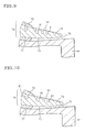
- the thin portion 66 whose middle portion has a shape bent toward the cavity 48 as shown in FIGS. 2 and 5 or whose section of the thickness direction has a W shape as shown in FIGS. 1 and 4 is preferable in that the flexural displacement is large.
- the thin portion having the latter W-shaped section is especially preferable.
- the thin portion 66 having the bent shape as shown in FIGS. 2 and 5 or the W shape as shown in FIGS. 1 and 4 can be formed by using shrinkage of a piezoelectric/electrostrictive film in a short direction at a time of a sintering step of the piezoelectric/electrostrictive layer 73, or by adjusting a sintering shrinkage start timing or sintering shrinkage of upper and lower portions of the piezoelectric/electrostrictive layer 73, or further the shape of the thin portion 66.
- the thickness of the thin portion 66 is preferably set to such a range that mechanical strength of the device is secured and the flexural displacement of the piezoelectric/electrostrictive layer 73 is further prevented from being deteriorated by an increase of rigidity.
- the thickness is in a range of preferably 1 ⁇ m to 50 ⁇ m, more preferably 3 to 50 ⁇ m, especially preferably 3 to 12 ⁇ m.
- the thickness of the fixing portion 68 is preferably 10 ⁇ m or more, more preferably 50 ⁇ m or more.
- the shape of the surface of the substrate 44 on which the piezoelectric/electrostrictive operation portion 78 is laid is not especially limited to the rectangular shape.
- the surface may also be formed in a circular shape, or a polygonal shape other than a square shape, such as a triangular shape.
- the substrate 44 in the present invention may be formed of the ceramic, but is preferably constituted of a material which does not change in properties at a time of a heating treatment of the piezoelectric/electrostrictive layer 73 or the electrodes 75, 77 stacked on the thin portion 66 and which is superior in heat resistance and chemical stability.
- the substrate 44 is preferably formed of an electric insulation material so that a wiring connected to the lower electrode 77 formed on the substrate 44 is electrically disconnected.
- examples of the material include at least one material selected from a group consisting of (stabilized) zirconium oxide, aluminum oxide, magnesium oxide, titanium oxide, cerium oxide, spinel, mullite, aluminum nitride, silicon nitride, and glass.
- the material containing stabilized zirconium oxide is preferable in that the mechanical strength is high, tenacity is superior, and the durability of the thin portion 66 including a thin structure and loaded with vibration can therefore be improved, and that chemical stability is high and reactivity with the piezoelectric/electrostrictive layer 73 or the electrodes 75, 77 is remarkably small.
- examples of stabilized zirconium oxide may contain stabilizers such as calcium oxide, magnesium oxide, yttrium oxide, scandium oxide, ytterbium oxide, cerium oxide, and rare earth metal oxide.
- the amount of yttrium oxide or ytterbium oxide is preferably 1 to 30 mol%, more preferably 1.5 to 10 mol%.
- the amount of cerium oxide is preferably 6 to 50 mol%, more preferably 8 to 20 mol%.
- the amount of calcium oxide or magnesium oxide is preferably 5 to 40 mol%, more preferably 5 to 20 mol%.
- yttrium oxide is especially preferably added in an amount of preferably 1.5 to 10 mol%, especially preferably 2 to 4 mol%.
- the thin portion 66 may contain the ceramic as described above, and further contain components such as silicon oxide or boron oxide contained in clay for use as a sintering aid.
- silicon oxide or boron oxide contained in clay is in a range of preferably 20% or less by mass, more preferably 3% or less by mass in the thin portion 66.
- the ceramic constituting the thin portion 66 has an average particle diameter of crystal grains in a range of preferably 0.05 to 2 ⁇ m, more preferably 0.1 to 1 ⁇ m in order to enhance the mechanical strength of the thin portion 66.
- the electrodes 75, 77 (75 to 77) in the present invention are electrically connected to the piezoelectric/electrostrictive layer 73 (71, 72).
- a pair of flat film shaped electrodes 75, 77 may be stacked on the upper and lower surfaces of the piezoelectric/electrostrictive layer 73.
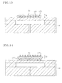
- modification examples include one pair of comb-shaped electrodes 175, 177 formed on the upper surface of the piezoelectric/electrostrictive layer 73 as shown in FIGS. 11 and 12, and one pair of comb-shaped electrodes 175, 177 formed the lower surface of the piezoelectric/electrostrictive layer 73 as shown in FIG. 13.
- a single flat film shaped electrode 277 is formed in the lower surface of the piezoelectric/electrostrictive layer 73, and a plurality of band-shaped electrodes 275 are formed in the upper surface of the piezoelectric/electrostrictive layer 73.
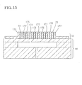
- one pair of comb-shaped electrodes 175, 177 are embedded in the piezoelectric/electrostrictive layer 73, and the respective electrodes 175, 177 are alternately disposed in a plurality of segments of the piezoelectric/electrostrictive layer 73 divided in a field direction.
- a multilayered piezoelectric/electrostrictive film type device 20 as shown in FIGS. 4 to 6.
- a plurality of piezoelectric/electrostrictive layers 71, 72 and electrodes 75 to 77 are disposed, and the respective electrodes 75 to 77 are preferably alternately held between the piezoelectric/electrostrictive layers 71, 72 to constitute the piezoelectric/electrostrictive film type device.
- the piezoelectric/electrostrictive film type device shown in FIGS. 11 to 14 has an advantage that power consumption can be reduced.
- the piezoelectric/electrostrictive film type device shown in FIG. 15 includes a structure in which an inverse piezoelectric effect of the field direction large in strain and generation force can effectively be used, and is advantageous in causing large displacement.
- the thicknesses of the electrodes 75, 77 (75 to 77) shown in FIG. 1 are set to be appropriate in accordance with applications. However, if the thickness is excessively large, the electrodes function as a relaxation layer. Since the flexural displacement tends to be reduced, the thickness is preferably 15 ⁇ m or less, more preferably 5 ⁇ m or less.
- the electrodes 75, 77 are preferably formed of materials which are solid at room temperature and which can withstand a high-temperature oxidation atmosphere at a time of sintering and integrating the electrodes and the substrate and/or the piezoelectric/electrostrictive layer and which is superior in electric conductivity.
- the materials include aluminum, titanium, chromium, iron, cobalt, nickel, copper, zinc, niobium, molybdenum, ruthenium, palladium, rhodium, silver, tin, tantalum, tungsten, iridium, platinum, gold, lead, and another simple metal or an alloy containing one of the metals mentioned above.
- a cermet material may also be used in which the materials constituting the piezoelectric/electrostrictive layer, or the material constituting the substrate 44 such as zirconium oxide, cerium oxide, and titanium oxide are dispersed in the metals described above.
- the materials of the electrodes 75, 77 (75 to 77) in the present invention are preferably selected in consideration of a method of forming the piezoelectric/electrostrictive layer 73 (71, 72).
- the upper electrode 75 can be formed on the piezoelectric/electrostrictive layer 73 at a low temperature (the electrode 75 positioned in an uppermost layer in the multilayered piezoelectric/electrostrictive film type device 20 shown in FIGS. 4 to 6). Therefore, in addition to the high-melting metals, low-melting metals such as aluminum, gold, and silver may also be used.
- the electrode 77 positioned in the lowermost layer, and the intermediate electrode 76 disposed between the piezoelectric/electrostrictive layers 71, 72 are also preferably constituted of electrode materials which contain platinum as a major component and further contain additives such as zirconium oxide, cerium oxide, and titanium oxide.
- the electrodes and piezoelectric/electrostrictive device constituted of these materials can be prevented from peeling.
- the additives are preferably contained in all the electrode materials in an amount of 0.01 to 20% by mass in that a desired peel preventive effect is obtained.
- examples of the method of forming the electrodes include ion beam, sputtering, vacuum deposition, PVD, ion plating, CVD, plating, screen printing, spraying, and dipping.
- the outer surface of the piezoelectric/electrostrictive layer 73 includes a highly water repellent surface for inhibiting the moisture 91 from infiltrating into the micro-pores 81 opened in the outer surface, or the gap 70 between the substrate 44 and the piezoelectric/electrostrictive layer 73 (71, 72).
- the surface modification in the present specification means that the ceramic or metal constituting the piezoelectric/electrostrictive layer or electrode and existing in the outer surface of the piezoelectric/electrostrictive layer or electrode changes into a chemical structure in which water repellency increases. Since the ceramic or metal constituting the piezoelectric/electrostrictive layer or electrode is not physically shielded from outside air, the outer surface is based on a concept different from that of a coat for physically shielding the ceramic or metal constituting the piezoelectric/electrostrictive layer from the outside air. It is to be noted that in FIGS. 7 to 10, portions subjected to the surface modification are shown by broken lines.
- examples of the piezoelectric/electrostrictive layer 73 (71, 72) or electrode 75 subjected to the surface modification include a structure in which a fluorine-based polymer compound is chemically bonded to the ceramic or metal constituting the piezoelectric/electrostrictive layer and fluorine elements are arranged in the surface of the piezoelectric/electrostrictive layer or electrode.
- the surface modification can be performed, for example, by coating the surface of the piezoelectric/electrostrictive layer 73 or electrode 75 with a surface modifier containing the fluorine-based polymer compound as the major component to chemically bond the fluorine-based polymer compound to the ceramic or metal.
- examples of the surface modifier for use in this case include: the fluorine-based polymer compound dissolved in hydrofluoroether; the fluorine-based polymer compound dissolved in hydrofluoroether and further mixed with dispersed polytetrafluoroethylene (PTFE); a silicone solution containing metaxylene hexafluoride as the major component; an acetic ether solution of 3, 3, 3-trifluoropropyl trimethoxysilane and the fluorine-based polymer compound.
- PTFE dispersed polytetrafluoroethylene
- the fluorine-based polymer compound dissolved in hydrofluoroether is preferable in that the water repellency is good.
- the fluorine-based polymer compound dissolved in hydrofluoroether and further mixed with dispersed polytetrafluoroethylene (PTFE) is more preferable in that the water repellency is good.
- a solid content concentration of the fluorine-based polymer compound is preferably 0.1 to 10%, more preferably 0.2 to 5%, further preferably 1 to 4%, and especially preferably 2 to 3% in that diffusive properties of the surface modifier at a coating time are superior and a water repellent effect is great after the surface modification.
- the surface modifier for use in the present invention may be colorless/transparent, but may also be mixed with a colorant and preferably colored in order to securely identify a region subjected to the surface modification.
- organo-silane KBM-7103 manufactured by Shin-Etsu Chemical Co., Ltd.
- CT-301S-2 manufactured by Kabushiki Kaisha Asahi Kagaku Kenkyusho.
- the portion including at least the piezoelectric/electrostrictive layer may be coated with the above-described surface modifier.
- the coating method at this time include a spin coating method, dipping method, brush coat method, dispenser method, and ink jet method.
- the surface of the substrate on a side opposite to the surface in which the piezoelectric/electrostrictive layer is disposed is covered with a UV sheet lest any portion of the surface modifier should not stick thereon as a result of spreading throughout from the coated portion.
- the device is fixed to a sample stage.
- the number of rotations of the sample stage is raised to 1000 to 3000 rpm, and the stage may be rotated for about ten seconds to five minutes.
- the surface of the piezoelectric/electrostrictive device may be coated with the surface modifier with a brush.
- the surface modifier for use in the present invention usually has a very small surface tension in the surface of the piezoelectric/electrostrictive layer.
- the surface modifier naturally infiltrates into the micro-pores opened in the surface of the piezoelectric/electrostrictive layer, or into the gap between the piezoelectric/electrostrictive layer and the substrate.
- the modification treatment of the surface properties is completed.
- the excessive surface modifier is preferably removed.
- the spin coating method is preferable, because the excessive surface modifier can be removed by a rotation force at the time of the coating with the surface modifier.
- compressed air may also be sprayed to remove the excessive surface modifier.
- the outer surface of the piezoelectric/electrostrictive layer 73 or electrode 75 is modified into the highly water repellent surface.
- the surface modification may be performed to such an extent that the moisture 91 is inhibited from infiltrating into the micro-pores 81 opened in the outer surface of the piezoelectric/electrostrictive layer 73 or electrode 75, or into the gap (non-bonded portion) 70 between the substrate 44 and piezoelectric/electrostrictive layer 73.
- the whole outer surface of the piezoelectric/electrostrictive layer 73 including the inner surface of the micro-pore 81 opened in the outer surface of the piezoelectric/electrostrictive layer 73 is preferably modified.
- FIGS. 7, 8 only the piezoelectric/electrostrictive layer 73 (71, 72) or the electrode 75 may be subjected to the surface modification (the drawings show that only the piezoelectric/electrostrictive layer is subjected to the surface modification). Additionally, as shown in FIG. 9, one of the micro-pores 81 reaches the piezoelectric/ electrostrictive layer through the electrode. Therefore, to more securely prevent the dielectric breakdown, not only the piezoelectric/electrostrictive layer 73 but also the upper electrode 75 are preferably subjected to the surface modification. As shown in FIG. 10, the surface of the substrate 44 in which the piezoelectric/electrostrictive layer is laid is further modified.
- weather resistances moisture resistance, light resistance, acid resistance, contamination resistance
- the moisture can preferably be inhibited from infiltrating between the substrate 44 and the piezoelectric/electrostrictive layer 73.
- the piezoelectric/electrostrictive layer 73 may not necessarily include the projecting portion 79 shown in FIGS. 1 to 6, but the projecting portion 79 is preferably disposed so as to secure the insulation between the electrodes.
- the piezoelectric/electrostrictive layer 73 including the projecting portion 79 is disposed, the projecting portion 79 may completely be detached from the substrate, or may partially be bonded to the substrate.
- the present invention can especially preferably be applied to the piezoelectric/electrostrictive film type device 10 in which the piezoelectric/electrostrictive layer 73 including the projecting portion 79 is disposed.
- the material of the piezoelectric/electrostrictive layer 73 may be crystalline or amorphous as long as field inducing strains such as piezoelectric or electrostrictive effects are caused. Any of a semiconductor, ceramic, ferroelectric ceramic, and antiferroelectric ceramic may be used, and the material may appropriately be selected/used in accordance with the application.
- the material include the ceramic containing one or two or more of lead zirconate, lead titanate, lead zirconate titanate, lead magnesium niobate, lead nickel niobate, lead zinc niobate, lead manganese niobate, lead antimony stannate, lead manganese tungstate, lead cobalt niobate, barium titanate, sodium bismuth titanate, potassium sodium niobate, and strontium bismuth tantalite.
- a material containing lead zirconate titanate (PZT-system) and lead magnesium niobate (PMN-system) as the major components, or sodium bismuth titanate as the major component is especially preferable, in that stabilized composition having a high electromechanical coupling coefficient and piezoelectric constant and little reactivity with the ceramic substrate at the sintering time of the piezoelectric/electrostrictive film is obtained.
- a material may also be used including the ceramic material containing a small amount of components to which at least one alone or two or more oxides of lantern, calcium, strontium, molybdenum, tungsten, barium, niobium, zinc, nickel, manganese, cerium, cadmium, chromium, cobalt, antimony, iron, yttrium, tantalum, lithium, bismuth, and tin are added.
- lantern or strontium is contained in lead zirconate, lead titanate, and lead magnesium niobate as the major components, advantages can sometimes be obtained that anti-electric field or piezoelectric property can be adjusted.
- the thickness of the piezoelectric/electrostrictive layer 73 shown in FIGS. 1, and the like is preferably set to be substantially equal to that of the substrate 44 in that the mechanical strength and desired flexural displacement of the device can be secured.
- a ratio of the thickness to that of the thin portion 66 of the substrate 44 (the thin portion/(the piezoelectric/electrostrictive layer)) is preferably 0.1 to 30, more preferably 0.3 to 10, and especially preferably 0.5 to 5.
- the substrate 44 (the thin portion 66) easily follows the sintering shrinkage of the piezoelectric/electrostrictive layer 73 at a time of the coating of the substrate 44 with the piezoelectric/ electrostrictive material and the subsequent heating treatment for forming the piezoelectric/electrostrictive layer 73.
- the substrate can be integrated with the dense piezoelectric/electrostrictive layer 73 without causing the peel. A sufficient resistance to the vibration by the bending of the piezoelectric/electrostrictive layer 73 can be imparted.
- the thickness of the piezoelectric/electrostrictive layer 73 is preferably 5 to 100 ⁇ m, more preferably 5 to 50 ⁇ m, and especially preferably 5 to 30 ⁇ m.
- the piezoelectric/electrostrictive film type device 20 shown in FIGS. 4 to 6 is formed in a thin film shape. Then, an aspect ratio can be raised.
- the thickness per layer in the piezoelectric/electrostrictive layers 71, 72 is preferably set to 30 ⁇ m or less.
- a plurality of piezoelectric/electrostrictive layers 71, 72 are preferably formed so that the layers gradually become thin in order from the lower layer.
- the layers are preferably formed so that a thickness t n of an n-th piezoelectric/electrostrictive layer from below satisfies the following equation: t n ⁇ t n-1 ⁇ 0.95.
- the strain of the piezoelectric/electrostrictive layer is large at the same driving voltage, when the piezoelectric/electrostrictive layer has a small thickness. Therefore, the upper piezoelectric/electrostrictive layer is formed so that the layer is strained more than the lower piezoelectric/electrostrictive layer. Accordingly, a bending efficiency is improved, and the flexural displacement can more effectively be developed.
- the piezoelectric/electrostrictive layer 73 in the present invention for example, after the piezoelectric/electrostrictive material including the above-described ceramic material is stacked on the lower electrode 77 formed in the substrate 44 (after each of the piezoelectric/electrostrictive layers 71, 72 is stacked or after all of the piezoelectric/electrostrictive layers 71, 72 are stacked in the multilayered piezoelectric/electrostrictive device 20 shown in FIGS. 4 to 6), a heat treatment is performed at a predetermined temperature.
- the piezoelectric/electrostrictive material for use in the present invention can be prepared, for example, by an oxide mixing method, coprecipitation method, alcoxide method, and the like.
- examples of the method of applying the piezoelectric/electrostrictive material include: various thick-film forming methods such as a screen printing method, dipping method, coat method, and electrophoretic migration method; and various thin-film forming methods such as an ion beam method, sputtering method, vacuum deposition method, ion plating method, chemical vapor deposition method (CVD), and plating.
- various thick-film forming methods such as a screen printing method, dipping method, coat method, and electrophoretic migration method
- various thin-film forming methods such as an ion beam method, sputtering method, vacuum deposition method, ion plating method, chemical vapor deposition method (CVD), and plating.
- the thick-film forming methods such as the screen printing method, dipping method, coat method, and electrophoretic migration method are preferable.
- the piezoelectric/electrostrictive material may be printed or applied in a broader range so as to coat the upper and lower surfaces of the respective electrodes.
- the projecting portion 79 of the piezoelectric/electrostrictive layer can be set to a completely non-bonded state with respect to the substrate 44.
- the electrode 77 is stacked on the substrate 44, thereafter the piezoelectric/electrostrictive materials are stacked alternately with the plurality of electrodes 75, 76 by the above-described various methods, and finally the electrode 75 may be disposed.
- the heating treatment may be performed at a temperature of 1000 to 1400°C.
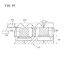
- the piezoelectric/electrostrictive film type device and the manufacturing method of the device according to the present invention have been described above, but the piezoelectric/electrostrictive film type device of the present invention can be used, for example, as a driving portion 120 of a display device or ink jet printer head as shown in FIGS. 18, 19. Concretely, as shown in FIG. 18, a light guide plate 200 for introducing a light 180 from a light source 160 is disposed. Additionally, the driving portion 120 including the piezoelectric/electrostrictive film type device 10 of the present invention as a main constituting element is disposed opposite to the rear surface of the light guide plate 200, and opposite to a pixel.
- the driving portion 120 including the piezoelectric/electrostrictive film type device 10 of the present invention as the main constituting element and including a pressurizing chamber 100 constituted of the cavity 48 of the substrate 44 is integrally bonded to an ink nozzle member 111 including a nozzle 112 opened to the outside from the pressurizing chamber 100 of the driving portion 120 through a channel for ink jet 117, and an orifice 114 opened into the pressurizing chamber 100 of the driving portion 120 from an ink supply source through a channel for ink supply 118.
- the ink jet printer head can be constituted.
- the contents of JP-A-2001-343598 and JP-A-11-147318 are incorporated herein by reference
- Example The present invention will concretely be described hereinafter by examples of a piezoelectric film type device, but the present invention is not limited to these examples. It is to be noted that evaluation was performed as follows with respect to each example and comparative example.
- a bath having a constant temperature and humidity was used to evaluate insulation resistance at an application time of direct current of 40 V at a temperature of 27°C and humidity of 90%.
- a platinum-made lower electrode (dimension: 1.2 ⁇ 0.8 mm, thickness: 3 ⁇ m) was formed on a substrate whose thin portion and fixing portion were both made of Y 2 O 3 -stabilized ZrO 2 (dimension of the thin portion: 1.6 ⁇ 1.1 mm, thickness: 10 ⁇ m) by the screen printing method.
- the heat treatment at a temperature of 1300°C for 2 hours was carried out to integrate the electrode with the substrate.
- a piezoelectric material constituted of ( Pb 0 ⁇ 999 La 0 ⁇ 001 ) (Mg 1/3 Nb 2/3 ) 0.375 Ti 0.375 Zr 0 ⁇ 250 O 3 in which a part of Pb was substituted with 0.1 mol% of La (average particle diameter of 0.49 ⁇ m, maximum particle diameter of 1.8 ⁇ m) was laminated in a thickness of 20 ⁇ m in a broader range of 1.3 ⁇ 0.9 mm including the surface disposed opposite to the upper surface of the lower electrode by the screen printing method.
- the atmosphere-controlling material having the same composition as that of the piezoelectric material was placed in a container, and the laminate of the piezoelectric material on the electrode-formed substrate was heat-treated at 1275°C for two hours.
- the thickness of the piezoelectric layer after the heat treatment was 13 ⁇ m.
- the upper electrode of gold was formed in a thickness of 0.5 ⁇ m in a range of 1.2 ⁇ 0.8 mm on the piezoelectric layer by the screen printing method, and heat-treated at 60°C.
- a portion of the obtained device on a side opposite to a surface of the substrate in which the piezoelectric/electrostrictive layer and electrode were disposed was covered with a UV sheet lest any portion of the surface modifier should not stick thereon as a result of spreading throughout from the coated portion and fixed onto a sample stage.
- the whole device was coated with the surface modifier of the fluorine-based polymer compound dissolved in hydrofluoroether (RFH-01 manufactured by Hishie Kagaku Kabushiki Kaisha (the solid content concentration of the fluorine-based polymer compound: 2%) by the spin coating method. In this case, immediately after dropping the coat solution, the rotation number was increased to 2000 rpm, and the sample stage was rotated for 30 seconds.
- the device coated with the surface modifier was left to stand at room temperature for 10 minutes. Thereafter, the surfaces of the piezoelectric/electrostrictive layer, substrate, and upper electrode were subjected to the modification treatment. Accordingly, the piezoelectric/electrostrictive film type device having a high water repellency was manufactured.
- the piezoelectric/electrostrictive film type device was manufactured in the same manner as in Example 1 except that the fluorine-based polymer compound dissolved in hydrofluoroether by an amount of 1% (solid content concentration) (RFH-02 manufactured by Hishie Kagaku Kabushiki Kaisha) was used as the surface modifier.
- fluorine-based polymer compound dissolved in hydrofluoroether by an amount of 1% (solid content concentration) (RFH-02 manufactured by Hishie Kagaku Kabushiki Kaisha) was used as the surface modifier.
- the piezoelectric/electrostrictive film type device was manufactured in the same manner as in Example 1 except that the fluorine-based polymer compound dissolved in hydrofluoroether by an amount of 0.2% (solid content concentration) (RFH-10 manufactured by Hishie Kagaku Kabushiki Kaisha) was used as the surface modifier.
- fluorine-based polymer compound dissolved in hydrofluoroether by an amount of 0.2% (solid content concentration) (RFH-10 manufactured by Hishie Kagaku Kabushiki Kaisha) was used as the surface modifier.
- the piezoelectric/electrostrictive film type device was manufactured in the same manner as in Example 1 except that the fluorine-based polymer compound dissolved in hydrofluoroether by an amount of 0.3% (solid content concentration) and further mixed with the colorant (RFH-10 manufactured by Hishie Kagaku Kabushiki Kaisha) was used as the surface modifier.
- the fluorine-based polymer compound dissolved in hydrofluoroether by an amount of 0.3% (solid content concentration) and further mixed with the colorant (RFH-10 manufactured by Hishie Kagaku Kabushiki Kaisha) was used as the surface modifier.
- the piezoelectric/electrostrictive film type device was manufactured in the same manner as in Example 1 except that the fluorine-based polymer compound dissolved in hydrofluoroether by an amount of 1% (solid content concentration) and further mixed with dispersed polytetrafluoroethylene (PTFE) by 0.2% (solid content concentration) (total solid content concentration of 1.2%) (RFH-10P manufactured by Hishie Kagaku Kabushiki Kaisha) was used as the surface modifier.
- PTFE polytetrafluoroethylene
- the piezoelectric/electrostrictive film type device was manufactured in the same manner as in Example 1 except that the silicone solution containing metaxylene hexafluoride as the major component (KP-801M manufactured by Shin-Etsu Chemical Co., Ltd., 95% or more of metaxylene hexafluoride) was used as the surface modifier.
- the silicone solution containing metaxylene hexafluoride as the major component KP-801M manufactured by Shin-Etsu Chemical Co., Ltd., 95% or more of metaxylene hexafluoride
- the piezoelectric/electrostrictive film type device was manufactured in the same manner as in Example 1 except that 3, 3, 3-trifluoropropyl trimethoxysilane (organo-silane KBM-7103 manufactured by Shin-Etsu Chemical Co., Ltd.) was used as the surface modifier.
- the piezoelectric/electrostrictive film type device was manufactured in the same manner as in Example 1 except that the acetic ether solution (CT-301S-2 manufactured by Kabushiki Kaisha Asahi Kagaku Kenkyusho) was used as the surface modifier.
- CT-301S-2 manufactured by Kabushiki Kaisha Asahi Kagaku Kenkyusho
- the piezoelectric/electrostrictive film type device was manufactured in the same manner as in Example 1 except that the surface modification was not performed.
- the piezoelectric/electrostrictive film type device was manufactured in the same manner as in Example 1 except that a coat agent formed of a silicone resin was applied instead of the surface modifier.
- the direct-current resistance did not drop before/after disposing the device in the constant temperature/humidity bath.
- the flexural displacement before disposing the device in the constant temperature/humidity bath did not drop at all even as compared with the piezoelectric/electrostrictive film type device of Comparative Example 1 not including any coat layer.
- the piezoelectric/electrostrictive film type device in which the flexural displacement is not reduced and in which the dielectric breakdown or peel of the piezoelectric/electrostrictive layer does not occur and which is superior in durability.
- the piezoelectric/electrostrictive film type device in which the number of piezoelectric/electrostrictive layers is small, the driving of the piezoelectric/electrostrictive layer is hardly restricted and the flexural displacement is hardly reduced as compared with the piezoelectric/electrostrictive film type device in which the piezoelectric/electrostrictive layer is coated.
Landscapes
- Particle Formation And Scattering Control In Inkjet Printers (AREA)
- General Electrical Machinery Utilizing Piezoelectricity, Electrostriction Or Magnetostriction (AREA)
Applications Claiming Priority (4)
| Application Number | Priority Date | Filing Date | Title |
|---|---|---|---|
| US39891702P | 2002-07-26 | 2002-07-26 | |
| US398917P | 2002-07-26 | ||
| JP2003165334A JP2004064067A (ja) | 2002-07-26 | 2003-06-10 | 圧電/電歪膜型素子 |
| JP2003165334 | 2003-06-10 |
Publications (2)
| Publication Number | Publication Date |
|---|---|
| EP1387416A2 true EP1387416A2 (fr) | 2004-02-04 |
| EP1387416A3 EP1387416A3 (fr) | 2006-03-22 |
Family
ID=31946698
Family Applications (1)
| Application Number | Title | Priority Date | Filing Date |
|---|---|---|---|
| EP03254612A Withdrawn EP1387416A3 (fr) | 2002-07-26 | 2003-07-24 | Composant à couche piézoélectrique/électrostrictive |
Country Status (3)
| Country | Link |
|---|---|
| US (1) | US20040032186A1 (fr) |
| EP (1) | EP1387416A3 (fr) |
| JP (1) | JP2004064067A (fr) |
Cited By (1)
| Publication number | Priority date | Publication date | Assignee | Title |
|---|---|---|---|---|
| EP2091091A3 (fr) * | 2008-02-14 | 2011-12-21 | NGK Insulators, Ltd. | Élément piézoélectrique/électrostrictif et son procédé de fabrication |
Families Citing this family (8)
| Publication number | Priority date | Publication date | Assignee | Title |
|---|---|---|---|---|
| US7332851B2 (en) | 2004-09-29 | 2008-02-19 | Ngk Insulators, Ltd. | Piezoelectric/electrostrictive film type device and method of manufacturing the same |
| WO2006035723A1 (fr) * | 2004-09-29 | 2006-04-06 | Ngk Insulators, Ltd. | Element de type film piezoelectrique/d'electrostriction et procede de fabrication de celui-ci |
| JP5398131B2 (ja) * | 2006-07-14 | 2014-01-29 | キヤノン株式会社 | 圧電体素子、圧電体の製造方法及び液体噴射ヘッド |
| CA2654688C (fr) * | 2006-12-09 | 2011-07-26 | Murata Manufacturing Co., Ltd. | Pompe piezoelectrique |
| JP2009086050A (ja) * | 2007-09-27 | 2009-04-23 | Brother Ind Ltd | 光圧電変換素子、アクチュエータ、センサー、光走査装置及び光走査型表示装置 |
| JP5788137B2 (ja) * | 2009-11-20 | 2015-09-30 | 株式会社リコー | 電気−機械変換膜の作製方法、電気−機械変換膜を備えた電気−機械変換素子、該素子を有する液体吐出ヘッド、液体吐出ヘッドを有する液体吐出装置 |
| JP5229242B2 (ja) * | 2010-01-20 | 2013-07-03 | ブラザー工業株式会社 | 光スキャナ |
| JP6269259B2 (ja) * | 2014-03-31 | 2018-01-31 | ブラザー工業株式会社 | 液体噴射装置の製造方法、液体噴射装置、及び、撥液層形成方法 |
Family Cites Families (10)
| Publication number | Priority date | Publication date | Assignee | Title |
|---|---|---|---|---|
| JPH03221527A (ja) * | 1990-01-29 | 1991-09-30 | Oki Electric Ind Co Ltd | 圧電子保護膜 |
| JP3120260B2 (ja) * | 1992-12-26 | 2000-12-25 | 日本碍子株式会社 | 圧電/電歪膜型素子 |
| JP3318687B2 (ja) * | 1993-06-08 | 2002-08-26 | 日本碍子株式会社 | 圧電/電歪膜型素子及びその製造方法 |
| JPH09181558A (ja) * | 1995-12-27 | 1997-07-11 | Kyocera Corp | 圧電素子及び樹脂封止型圧電部品 |
| US6495624B1 (en) * | 1997-02-03 | 2002-12-17 | Cytonix Corporation | Hydrophobic coating compositions, articles coated with said compositions, and processes for manufacturing same |
| US5822170A (en) * | 1997-10-09 | 1998-10-13 | Honeywell Inc. | Hydrophobic coating for reducing humidity effect in electrostatic actuators |
| JP3826608B2 (ja) * | 1999-03-17 | 2006-09-27 | 富士写真フイルム株式会社 | 液体吐出部表面の撥水膜形成 |
| JP4031624B2 (ja) * | 2000-06-23 | 2008-01-09 | 株式会社東芝 | 透明被膜付基材、透明被膜形成用塗布液、および表示装置 |
| US6515402B2 (en) * | 2001-01-24 | 2003-02-04 | Koninklijke Philips Electronics N.V. | Array of ultrasound transducers |
| US7067961B2 (en) * | 2002-07-12 | 2006-06-27 | Ngk Insulators, Ltd. | Piezoelectric/electrostrictive film device, and manufacturing method of the device |
-
2003
- 2003-06-10 JP JP2003165334A patent/JP2004064067A/ja not_active Withdrawn
- 2003-07-17 US US10/622,871 patent/US20040032186A1/en not_active Abandoned
- 2003-07-24 EP EP03254612A patent/EP1387416A3/fr not_active Withdrawn
Cited By (2)
| Publication number | Priority date | Publication date | Assignee | Title |
|---|---|---|---|---|
| EP2091091A3 (fr) * | 2008-02-14 | 2011-12-21 | NGK Insulators, Ltd. | Élément piézoélectrique/électrostrictif et son procédé de fabrication |
| US8479364B2 (en) | 2008-02-14 | 2013-07-09 | Ngk Insulators, Ltd. | Piezoelectric/electrostrictive element and method of manufacturing the same |
Also Published As
| Publication number | Publication date |
|---|---|
| EP1387416A3 (fr) | 2006-03-22 |
| US20040032186A1 (en) | 2004-02-19 |
| JP2004064067A (ja) | 2004-02-26 |
Similar Documents
| Publication | Publication Date | Title |
|---|---|---|
| EP0615295B1 (fr) | Elément piézoélectrique électrostrictif comportant des couches d'électrode à rugosité spécifique de surface | |
| EP1998383B1 (fr) | Procede de fabrication d'un element en ceramique, element en ceramique pour dispositif de detection de gaz, dispositif de pile a combustible, dispositif filtrant, dispositif piezoelectrique multi-couche, injecteur et systeme d'injection de combustible | |
| US7902726B2 (en) | Multi-layer piezoelectric device | |
| US8378554B2 (en) | Multi-layer piezoelectric element and injection apparatus using the same | |
| CN1661827B (zh) | 压电元件及其制造方法、以及喷墨头和喷墨式记录装置 | |
| US7358653B2 (en) | Piezoelectric element | |
| JPH05267742A (ja) | 圧電/電歪膜型素子 | |
| JP2002100819A (ja) | 圧電体素子、及びその製造方法 | |
| EP1387416A2 (fr) | Composant à couche piézoélectrique/électrostrictive | |
| US7267840B2 (en) | Manufacturing method of piezoelectric/electrostrictive film type device | |
| US8339017B2 (en) | Multi-layer piezoelectric element and injection apparatus using the same | |
| US7067961B2 (en) | Piezoelectric/electrostrictive film device, and manufacturing method of the device | |
| JP4473529B2 (ja) | 圧電/電歪膜型素子、及びその製造方法 | |
| CN101271957A (zh) | 叠层型压电元件 | |
| JP2002009359A (ja) | 耐久性に優れた一体型圧電/電歪膜型素子およびその製造方法 | |
| JP2004186436A (ja) | 圧電/電歪膜型素子 | |
| US6102531A (en) | Piezoelectric film type actuator and ink jet printer head having the same | |
| EP1294030A2 (fr) | Dispositif piézo-électrique/électrostrictif | |
| JP2000252534A (ja) | 積層型圧電アクチュエータ | |
| JPH11284244A (ja) | 圧電/電歪膜型アクチュエータ | |
| US20090271963A1 (en) | Piezoelectric actuator and manufacturing method thereof, magnetic disk apparatus | |
| CN120225033A (zh) | 具有压电膜的层叠基板、层叠基板的制造方法和压电元件 | |
| JPH11346012A (ja) | 圧電/電歪膜型アクチュエータ |
Legal Events
| Date | Code | Title | Description |
|---|---|---|---|
| PUAI | Public reference made under article 153(3) epc to a published international application that has entered the european phase |
Free format text: ORIGINAL CODE: 0009012 |
|
| AK | Designated contracting states |
Kind code of ref document: A2 Designated state(s): AT BE BG CH CY CZ DE DK EE ES FI FR GB GR HU IE IT LI LU MC NL PT RO SE SI SK TR |
|
| AX | Request for extension of the european patent |
Extension state: AL LT LV MK |
|
| PUAL | Search report despatched |
Free format text: ORIGINAL CODE: 0009013 |
|
| AK | Designated contracting states |
Kind code of ref document: A3 Designated state(s): AT BE BG CH CY CZ DE DK EE ES FI FR GB GR HU IE IT LI LU MC NL PT RO SE SI SK TR |
|
| AX | Request for extension of the european patent |
Extension state: AL LT LV MK |
|
| AKX | Designation fees paid |
Designated state(s): DE FR GB |
|
| STAA | Information on the status of an ep patent application or granted ep patent |
Free format text: STATUS: THE APPLICATION IS DEEMED TO BE WITHDRAWN |
|
| 18D | Application deemed to be withdrawn |
Effective date: 20060923 |