EP1391987A1 - Reflexionsverlustunterdrückungsschaltung - Google Patents
Reflexionsverlustunterdrückungsschaltung Download PDFInfo
- Publication number
- EP1391987A1 EP1391987A1 EP02714506A EP02714506A EP1391987A1 EP 1391987 A1 EP1391987 A1 EP 1391987A1 EP 02714506 A EP02714506 A EP 02714506A EP 02714506 A EP02714506 A EP 02714506A EP 1391987 A1 EP1391987 A1 EP 1391987A1
- Authority
- EP
- European Patent Office
- Prior art keywords
- circuit
- reflection loss
- loss suppression
- transmission line
- frequency
- Prior art date
- Legal status (The legal status is an assumption and is not a legal conclusion. Google has not performed a legal analysis and makes no representation as to the accuracy of the status listed.)
- Withdrawn
Links
Images


Classifications
-
- H—ELECTRICITY
- H03—ELECTRONIC CIRCUITRY
- H03F—AMPLIFIERS
- H03F3/00—Amplifiers with only discharge tubes or only semiconductor devices as amplifying elements
- H03F3/60—Amplifiers in which coupling networks have distributed constants, e.g. with waveguide resonators
- H03F3/605—Distributed amplifiers
-
- H—ELECTRICITY
- H03—ELECTRONIC CIRCUITRY
- H03F—AMPLIFIERS
- H03F1/00—Details of amplifiers with only discharge tubes, only semiconductor devices or only unspecified devices as amplifying elements
- H03F1/08—Modifications of amplifiers to reduce detrimental influences of internal impedances of amplifying elements
- H03F1/22—Modifications of amplifiers to reduce detrimental influences of internal impedances of amplifying elements by use of cascode coupling, i.e. earthed cathode or emitter stage followed by earthed grid or base stage respectively
Definitions
- the present invention relates to a reflection loss suppression circuit for use in various microwave/milliwave circuits and digital circuits.
- microwave/milliwave circuits which perform the amplification, oscillation, mixing, etc. of radio frequency signals, and digital circuits which perform the amplification, identification, branch, etc. of digital signals have been put into practical use in various systems.
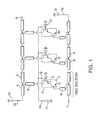
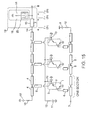
- Fig. 1 is a circuit diagram showing an example of the distributed amplifier in the prior art.
- the distributed amplifier in the prior art is a cascode-type distributed amplifier of three-stage configuration as employs HBT cascode pairs 3 each being constructed by cascode-connecting a hetero-junction bipolar transistor (hereinbelow, abbreviated to "HBT") 1 and an HBT 2.
- HBT hetero-junction bipolar transistor
- An input signal is received from an input terminal 7, while an output signal is delivered from an output terminal 8.
- the base terminal of the HBT 1 is fed with a DC supply voltage from a base power source 9 through a terminating resistor 12.
- the collector terminal of the HBT 2 is fed with a DC supply voltage from a collector power source 10 through a terminating resistor 12.
- the base terminal of the HBT 2 is fed with a DC supply voltage from a cascode power source 11 through a terminating resistor 12.
- the base terminal of the HBT 2 is grounded radio-frequency-wise through an RF grounding capacitor 13.
- the distributed amplifier stated above forms a transmission line of high cutoff frequency by combining the parasitic reactances of the HBTs 1 and HBTs 2- with high-impedance transmission lines 4 and 5.
- the transmission line has a characteristic impedance which is equal to each of a signal source impedance and a load impedance, and it can realize a flat gain and a low reflection loss over a wide band.
- the problems explained above are problems which can occur in various circuits such as microwave/milliwave circuits which perform the amplification, oscillation, mixing, etc. of radio frequency signals, and digital circuits which perform the amplification, identification, branch, etc: of digital signals.
- An object of the present invention is to connect a reflection loss suppression circuit to any of various circuits including a distributed amplifier, whereby a reflection loss outside a required frequency band is satisfactorily suppressed without degrading the characteristics of the circuit in the required frequency band, so as to attain the stability of the circuit.
- a reflection loss suppression circuit of the present invention comprises a transmission line which transforms an output impedance or an input impedance in a specified frequency band into a high impedance; and a resistance grounding circuit having a frequency selectivity, which is connected in parallel with the transmission line as viewed from an output terminal side or an input terminal side.
- the resistance grounding circuit includes a resistor having a predetermined resistance in the vicinity of a load resistance or a signal source resistance, and has a low impedance in the specified frequency band.
- the resistance grounding circuit is constructed of a circuit which is terminated by a one-terminal pair circuit having a high impedance outside the frequency band.
- the one-terminal pair circuit is constructed of an end-open stub which has a length equal to a quarter wavelength of a fundamental wave at any desired frequency included in the specified frequency band.
- the one-terminal pair circuit is constructed of a circuit in which a capacitance element is terminated by an end-open stub shorter by ⁇ than a half wavelength of a fundamental wave, when ⁇ is let denote a length being sufficiently small as compared with a wavelength ⁇ of the fundamental wave at any desired frequency included in the frequency band.
- the one-terminal pair circuit is constructed of a circuit in which an inductor element is terminated by an end-open stub longer by ⁇ than a half wavelength of a fundamental wave, when ⁇ is let denote a length being sufficiently small as compared with a wavelength ⁇ of the fundamental wave at any desired frequency included in the frequency band.
- ⁇ 0 corresponding to the frequency
- the transmission line and the end-open stub are formed by employing microstrip lines or coplanar lines.
- a reflection loss suppression circuit in the present invention comprises a transmission line which transforms an output impedance or an input impedance in a specified frequency band into a high impedance, and a resistance grounding circuit having a frequency selectivity, which is connected in parallel with the transmission line as viewed from an output terminal side or an input terminal side.
- the resistance grounding circuit is constructed of a circuit in which a band-pass filter for passing a signal of the frequency band is grounded through a resistor having a predetermined resistance in the vicinity of a load resistance or a signal source resistance.
- the band-pass filter is constructed of an interdigital capacitor which has a length equal to a quarter wavelength of a fundamental wave at any desired frequency included in the specified frequency band.
- An electric length. of the transmission line is set in a range of ⁇ 50% of an absolute value of an output impedance with the transmission line viewed.
- a resistance of the resistor constituting the resistance grounding circuit should preferably be set in a range of 0.5 through 2 times the load resistance or the signal source resistance.
- a wideband amplifier according to the present invention comprises the reflection loss suppression circuit at, at least, one of an output end and an input end.
- Fig. 2 is a circuit diagram showing an example in which the reflection loss suppression circuit in this embodiment is connected to the output end of a distributed amplifier.
- a portion except the reflection loss suppression circuit 19 has the same arrangement as that of the prior-art distributed amplifier shown in Fig.. 1, and the same reference numerals are assigned to the same parts.
- the reflection loss suppression circuit 19 in this embodiment is constructed of a transmission line 15 which is connected in series with the output end 14 of the distributed amplifier, and a resistance grounding circuit 18 which has a frequency selectivity and which is connected in parallel with the transmission line 15 as viewed from the side of the output terminal 8.
- the electric length ⁇ of the transmission line 15 is selected within a range of ⁇ 50% before and behind a value which maximizes the absolute value of an output impedance Z2 with the transmission line 15 viewed.
- the resistance grounding circuit 18 is constructed of a resistor 16, and a one-terminal pair circuit 17 which exhibits a low impedance in a frequency band to have a reflection loss suppressed therein and which exhibits a high impedance in any other frequency band.
- the resistance of the resistor 16 is selected within a range of 0.5 through 2 times a load resistance or a signal source resistance.
- an output impedance Z1 in the frequency band to have the reflection loss suppressed therein is transformed into the high impedance Z2 by the transmission line 15, and the resistance grounding circuit 18 is thereafter connected in parallel. Therefore, the output impedance Z3 of the whole circuit becomes substantially equal to the value of the resistor 16. Accordingly, the reflection loss can be suppressed by setting the resistance of the resistor 16 in the vicinity of the load resistance, concretely, within the range of 0.5 through 2 times the load resistance. Moreover, the above effect can be realized without affecting circuit characteristics outside the frequency band to have the reflection loss suppressed therein, by sufficiently heightening the frequency selectivity of the resistance grounding circuit 18, namely, the one-terminal pair circuit 17.
- Fig. 3 is a circuit diagram showing an example in which the reflection loss suppression circuit in this embodiment is connected to the output end of a distributed amplifier. Incidentally, the same reference numerals and signs are assigned to the same parts as in the reflection loss suppression circuit shown in Fig. 2.
- the reflection loss suppression circuit in this embodiment exhibits a low impedance in a frequency band to have a reflection loss suppressed therein.
- a one-terminal pair circuit 17 which exhibits a high impedance in any other frequency band, is constructed of an end-open stub 20 which has a length equal to the quarter wavelength of a fundamental wave for any desired frequency included in the first-mentioned frequency band.
- the "wavelength” termed here signifies the effective wavelength of an electromagnetic wave which propagates through the end-open stub.
- the reflection loss can be suppressed as in the first embodiment stated before. Moreover, the above effect can be realized without affecting circuit characteristics outside the frequency band to have the reflection loss suppressed therein, by sufficiently heightening the frequency selectivity of the one-terminal pair circuit 17.
- Fig. 4 is a circuit diagram showing an example in which the reflection loss suppression circuit in this embodiment is connected to the output end of a distributed amplifier.
- Fig. 5 is a circuit diagram of a resistance grounding circuit portion in' the reflection loss suppression circuit.
- Figs. 6 and 7 are diagrams for explaining the effects of the present invention.
- Figs. 8, 9, 10 and 11 are graphs showing simulation results concerning a case where the reflection loss suppression circuit in this embodiment is mounted, and a case where it is not mounted. Incidentally, the same reference numerals and signs are assigned to the same parts as in the reflection loss suppression circuit shown in Fig. 2.
- the reflection loss suppression circuit in this embodiment exhibits a low impedance in a frequency band to have a reflection loss suppressed therein.
- a one-terminal pair circuit 17 which exhibits a high impedance in any other frequency band, is constructed of a capacitor 21 .. and a ( ⁇ /2 - ⁇ )-long end-open stub 22.
- the ( ⁇ /2 - ⁇ )-long end-open stub 22 is an end-open stub which has a length shorter by ⁇ than the half wavelength of a fundamental wave for any desired frequency included in the first-mentioned frequency band.
- ⁇ denotes a length which is sufficiently short as compared with the wavelength ⁇ of the fundamental wave.
- the capacitance C of the capacitor 21, the length ⁇ , and the characteristic impedance Z 0 and propagation constant ⁇ of the ( ⁇ /2- ⁇ )-long end-open stub 22 are selected so as to satisfy Equation (1) below at an angular frequency ⁇ 0 corresponding to the frequency.
- Im[ ⁇ ] signifies to take the imaginary part of a complex number.
- Fig. 5 is the diagram showing the layout of a resistance grounding circuit 18 in the reflection loss suppression circuit 19 shown in Fig. 4.
- ⁇ denotes the attenuation constant of the end-open stub 22
- ⁇ denotes the phase constant thereof
- ⁇ ⁇ + j ⁇ holds.
- 1 ⁇ /2 - ⁇ holds
- Equation (4) two terms constituting the imaginary part of Equation (3) balance and cancel each other at the angle frequency ⁇ 0 .
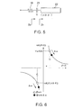
- - cot ⁇ 1 - 1 ⁇ 0 CZ 0
- the values of the two terms constituting the imaginary part of Equation (3) change in the directions of arrows in Fig. 6. Since the two values having balanced with positive and negative signs decrease simultaneously, the absolute value of the imaginary part of Equation (3) increases.
- the increasing rate of the above absolute value of the imaginary part in Equation (3), versus the frequency can be made a sufficiently large value by setting ⁇ to be sufficiently small as compared with the wavelength ⁇ of a fundamental wave. Accordingly, the frequency selectivity of the resistance grounding circuit 18 can be made satisfactorily high.
- This example handles a case where the absolute values of the reflection coefficients exceed one in the frequency band, that is, a case where a negative resistance has occurred.
- the ensuing description and the effects of the present invention hold quite true of a case where the absolute values of the reflection coefficients do not exceed one, that is, a case where the negative resistance has not occurred.
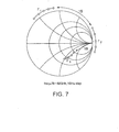
- the reflection coefficient ⁇ 1 as to which the reflection loss has increased and led to the occurrence of the negative resistance in the frequency band is moved near to a point at infinity on the Smith chart by the transmission line 15. That is; an input impedance Z1 is transformed into a high impedance Z2. Subsequently, the resistance grounding circuit 18 having the intense frequency selectivity is connected in parallel as stated before, whereby the reflection coefficient ⁇ 2 is transformed into ⁇ 3 near the center of the Smith chart. That is, the high impedance Z2 is transformed into an impedance Z3 which is close to a load impedance. Accordingly, the reflection loss in the frequency band is suppressed.
- Figs. 8 and 9 are graphs showing the simulation results of the frequency dependencies of again
- Figs. 10 and 11 are graphs showing the simulation results of the frequency dependencies of a stability factor and a stability measure, respectively, as to the case (the present invention) where the reflection loss suppression circuit in this embodiment is mounted, and the case (the prior art shown in Fig. 1) where it is not mounted.
- the stability factor is larger than one
- the stability measure is larger than zero
- the circuit has an absolute stability.
- the absolute stability is not attained in the case (the prior art) where the reflection loss suppression circuit is not mounted, whereas the absolute stability is attained by mounting the reflection loss suppression circuit in this embodiment.
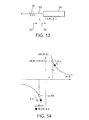
- Fig. 12 is a circuit diagram showing an example in which the reflection loss suppression circuit in this embodiment is connected to the output end of a distributed amplifier.
- Fig. 13 is a circuit diagram of a resistance grounding circuit portion in the reflection loss suppression circuit.
- Fig. 14 is a graph showing the simulation results concerning a case where the reflection loss suppression circuit in this embodiment is mounted, and a case where it is not mounted.
- the same reference numerals and signs are assigned to the same parts as-in the reflection loss suppression circuit shown in Fig. 2.
- the reflection loss suppression circuit in this embodiment exhibits a low impedance in a frequency band to have a reflection loss suppressed therein.
- a one-terminal pair circuit 17 which exhibits a high impedance in any other frequency band, is constructed of an. inductor 23 and a ( ⁇ /2 + ⁇ )-long end-open stub 24.
- the ( ⁇ /2 + ⁇ )-long end-open stub 24 is an end-open stub which has a length longer by ⁇ than the half wavelength of a fundamental wave for any desired frequency included in the first-mentioned frequency band.
- ⁇ denotes a length which is sufficiently short as compared with the wavelength ⁇ of the fundamental wave.
- the inductance L of the inductor 23, the length ⁇ , and the characteristic impedance Z 0 and propagation constant ⁇ of the ( ⁇ /2 + ⁇ )-long end-open stub 24 are selected so as to satisfy Equation (5) below at an angular frequency ⁇ 0 corresponding to the frequency.
- Im[ ⁇ ] signifies to take the imaginary part of a complex number.
- Fig. 13 is the diagram showing the layout of a resistance grounding circuit 18 in the reflection loss suppression circuit 19 shown in Fig. 12.
- An impedance Z i2 with the ( ⁇ /2 + ⁇ )-long end-open stub 24 and the inductor 23 viewed is calculated by Equation (6) below.
- 1 + ⁇ /2 + ⁇ holds.
- Z i2 j ⁇ L + Z 0 tanh( ⁇ 1 + )
- Equation (6) Assuming for the sake of description that the ( ⁇ /2 + ⁇ )-long end-open stub 24 is of low loss, Equation. (6). becomes Equation (7) below.
- ⁇ denotes the attenuation constant of the end-open stub 24
- ⁇ denotes the phase constant thereof
- Fig. 15 is a circuit diagram showing an example in which the reflection loss suppression circuit in this embodiment is connected to the output end of a distributed amplifier. Incidentally, the same reference numerals and signs are assigned to the same parts as in the reflection loss suppression circuit shown in Fig. 2.
- the reflection loss suppression circuit in this embodiment features. the point that a resistance grounding circuit 18 having a frequency selectivity is constructed of a circuit in which a band-pass filter 25 for passing the signal of a frequency band to have a reflection loss suppressed therein is grounded through a resistor 16.
- the reflection loss can be suppressed even by such a construction.
- the effects stated before can be realized without affecting circuit characteristics outside the frequency band to have the reflection loss suppressed therein, by sufficiently heightening the frequency selectivity of the band-pass filter 25.
- Fig. 16 is a circuit diagram showing an example in which the reflection loss suppression circuit in this embodiment is connected to the output end of a distributed amplifier. Incidentally, the same reference numerals and signs are assigned to the same parts as in the reflection loss suppression circuit shown in Fig. 15.
- the reflection loss suppression circuit in this embodiment features the point that the band-pass filter 25 in the fifth embodiment is constructed of an interdigital capacitor 26.
- the reflection loss can be suppressed even by such a construction.
- the effects stated before can be realized without affecting circuit characteristics outside a frequency band to have the reflection loss suppressed therein, by sufficiently heightening the frequency selectivity of the interdigital capacitor 26.
- the above embodiments have been described by exemplifying the distributed amplifier as the circuit from which the reflection loss is to be suppressed.
- the present invention is not restricted to the embodiments, but it is applicable in various circuits such as amplifiers, oscillators, mixers, frequency multipliers and frequency dividers of all types, and further, multifarious digital circuits as may be needed.
- the HBTs Hetero-junction Bipolar Transistors
- FETs such as MESFETs (Metal Semiconductor Field Effect Transistors) or HEMTs (High Electron Mobility Transistors), and silicon bipolar transistors.
- an output or input impedance in a frequency band to have a reflection loss suppressed therein is transformed into a high impedance by a transmission line having a suitable electric length, and a resistance grounding circuit having a high frequency selectivity is thereafter connected in parallel, whereby the reflection loss in the desired frequency band outside a required band can be reduced without affecting circuit characteristics in the required frequency band. Further, the stability of a circuit can be enhanced owing to the reduction of the reflection loss.
Landscapes
- Engineering & Computer Science (AREA)
- Power Engineering (AREA)
- Microwave Amplifiers (AREA)
- Amplifiers (AREA)
- Control Of Motors That Do Not Use Commutators (AREA)
Applications Claiming Priority (3)
| Application Number | Priority Date | Filing Date | Title |
|---|---|---|---|
| JP2001108775 | 2001-04-06 | ||
| JP2001108775A JP3865043B2 (ja) | 2001-04-06 | 2001-04-06 | 反射損失抑圧回路 |
| PCT/JP2002/003452 WO2002082640A1 (en) | 2001-04-06 | 2002-04-05 | Reflection loss suppression circuit |
Publications (2)
| Publication Number | Publication Date |
|---|---|
| EP1391987A1 true EP1391987A1 (de) | 2004-02-25 |
| EP1391987A4 EP1391987A4 (de) | 2006-01-25 |
Family
ID=18960852
Family Applications (1)
| Application Number | Title | Priority Date | Filing Date |
|---|---|---|---|
| EP02714506A Withdrawn EP1391987A4 (de) | 2001-04-06 | 2002-04-05 | Reflexionsverlustunterdrückungsschaltung |
Country Status (5)
| Country | Link |
|---|---|
| US (2) | US7129804B2 (de) |
| EP (1) | EP1391987A4 (de) |
| JP (1) | JP3865043B2 (de) |
| CN (1) | CN1256805C (de) |
| WO (1) | WO2002082640A1 (de) |
Families Citing this family (19)
| Publication number | Priority date | Publication date | Assignee | Title |
|---|---|---|---|---|
| JP4179091B2 (ja) * | 2003-07-28 | 2008-11-12 | 日本電気株式会社 | 電力分配回路及び周波数逓倍器 |
| JP2005159860A (ja) * | 2003-11-27 | 2005-06-16 | Mitsubishi Electric Corp | 広帯域増幅器 |
| JP4896609B2 (ja) * | 2005-07-15 | 2012-03-14 | 三菱電機株式会社 | フィードフォワード増幅器 |
| US7859803B2 (en) * | 2005-09-19 | 2010-12-28 | The Regents Of The University Of California | Voltage overload protection circuits |
| US7813092B2 (en) * | 2005-09-19 | 2010-10-12 | The Regents Of The University Of California | ESD unit protection cell for distributed amplifiers |
| JP2007158660A (ja) * | 2005-12-05 | 2007-06-21 | Alps Electric Co Ltd | 高周波回路 |
| US7400200B2 (en) * | 2006-03-17 | 2008-07-15 | Avago Technologies Wireless Ip Pte Ltd | Linear variable gain traveling wave amplifier |
| CN101136660B (zh) * | 2006-08-29 | 2012-04-18 | 中国电信股份有限公司 | 用于减少桥接抽头对电缆传输性能损伤的匹配吸收器 |
| JP4814943B2 (ja) * | 2006-08-31 | 2011-11-16 | 富士通株式会社 | データ送信回路、および送信方法 |
| JP4643666B2 (ja) * | 2008-02-22 | 2011-03-02 | 株式会社東芝 | 2次高調波抑圧フィルタ |
| US7880558B2 (en) * | 2008-08-29 | 2011-02-01 | Motorola, Inc. | Method and apparatus for adjusting load impedance of a distributed amplifier |
| JP5485068B2 (ja) * | 2010-08-02 | 2014-05-07 | 日本電信電話株式会社 | 分布増幅器 |
| US8786368B2 (en) * | 2011-03-09 | 2014-07-22 | Hittite Microwave Corporation | Distributed amplifier with improved stabilization |
| JPWO2013089163A1 (ja) * | 2011-12-14 | 2015-04-27 | 日本電気株式会社 | 共振回路、分布型増幅器、及び発振器 |
| US20180019510A1 (en) * | 2015-02-27 | 2018-01-18 | Nec Corporation | Termination circuit, wireless communication device and termination method |
| DE112016001629T5 (de) * | 2015-04-07 | 2018-01-04 | Mitsubishi Electric Corporation | Hochfrequenz-leistungsverstärker |
| JP2017017411A (ja) | 2015-06-29 | 2017-01-19 | 住友電気工業株式会社 | 進行波型増幅器 |
| US9602091B1 (en) * | 2015-12-03 | 2017-03-21 | Peregrine Semiconductor Corporation | Low phase shift, high frequency attenuator |
| CN114567270B (zh) * | 2022-04-29 | 2022-08-16 | 成都嘉纳海威科技有限责任公司 | 一种低成本线性功率放大器 |
Family Cites Families (14)
| Publication number | Priority date | Publication date | Assignee | Title |
|---|---|---|---|---|
| JPS601021A (ja) | 1983-06-16 | 1985-01-07 | Suzuki Motor Co Ltd | 幌付自動車の換気装置 |
| JPS601021U (ja) * | 1984-05-15 | 1985-01-07 | 富士通株式会社 | 導波管形トランジスタ増幅器 |
| JPH0683522B2 (ja) | 1985-12-23 | 1994-10-19 | 松下電工株式会社 | 制御盤 |
| JPS62147903U (de) * | 1986-03-13 | 1987-09-18 | ||
| JPH03218101A (ja) * | 1990-01-23 | 1991-09-25 | Fujitsu General Ltd | インターデジタルフィルタ |
| JPH05136639A (ja) * | 1991-04-08 | 1993-06-01 | Fujitsu Ten Ltd | 高周波用多段増幅回路 |
| JP2870714B2 (ja) * | 1991-09-12 | 1999-03-17 | 三菱電機株式会社 | マイクロ波増幅器 |
| JPH06147903A (ja) | 1992-11-06 | 1994-05-27 | Murata Mfg Co Ltd | 角速度センサ |
| JPH06164267A (ja) * | 1992-11-27 | 1994-06-10 | Toshiba Corp | 電力増幅器 |
| JPH0738349A (ja) * | 1993-07-19 | 1995-02-07 | Fujitsu Ltd | マイクロ波増幅器 |
| US5736901A (en) * | 1995-04-04 | 1998-04-07 | Matsushita Electric Industrial Co., Ltd. | Radio frequency amplifier with stable operation and restrained oscillation at low frequencies |
| JPH0969731A (ja) * | 1995-08-31 | 1997-03-11 | Mitsubishi Electric Corp | 周波数変換回路 |
| US5920230A (en) | 1997-10-21 | 1999-07-06 | Trw Inc. | HEMT-HBT cascode distributed amplifier |
| JP3175763B2 (ja) | 1998-10-06 | 2001-06-11 | 日本電気株式会社 | マイクロ波発振器 |
-
2001
- 2001-04-06 JP JP2001108775A patent/JP3865043B2/ja not_active Expired - Fee Related
-
2002
- 2002-04-05 EP EP02714506A patent/EP1391987A4/de not_active Withdrawn
- 2002-04-05 US US10/474,063 patent/US7129804B2/en not_active Expired - Fee Related
- 2002-04-05 WO PCT/JP2002/003452 patent/WO2002082640A1/ja not_active Ceased
- 2002-04-05 CN CN02811164.8A patent/CN1256805C/zh not_active Expired - Fee Related
-
2006
- 2006-06-07 US US11/447,838 patent/US7173502B2/en not_active Expired - Fee Related
Also Published As
| Publication number | Publication date |
|---|---|
| CN1513227A (zh) | 2004-07-14 |
| CN1256805C (zh) | 2006-05-17 |
| US20040239437A1 (en) | 2004-12-02 |
| US20060238269A1 (en) | 2006-10-26 |
| EP1391987A4 (de) | 2006-01-25 |
| JP2002305419A (ja) | 2002-10-18 |
| US7173502B2 (en) | 2007-02-06 |
| US7129804B2 (en) | 2006-10-31 |
| WO2002082640A1 (en) | 2002-10-17 |
| JP3865043B2 (ja) | 2007-01-10 |
Similar Documents
| Publication | Publication Date | Title |
|---|---|---|
| EP1391987A1 (de) | Reflexionsverlustunterdrückungsschaltung | |
| US5361038A (en) | Active load applications for distributed circuits | |
| US6346859B1 (en) | Microwave amplifier with reduced beat noise | |
| US8368483B2 (en) | Multiband matching circuit and multiband power amplifier | |
| JPH08130419A (ja) | 増幅器並びにこれを有する受信機及び通信機 | |
| US7245186B2 (en) | Bandpass amplifier | |
| US7123073B2 (en) | Amplifier and frequency converter | |
| JP3442208B2 (ja) | 高周波用電子回路 | |
| US6670801B2 (en) | Second harmonic tuning of an active RF device | |
| EP4466790B1 (de) | Kaskadierter rauscharmer breitbandiger aktiver phasenschieber | |
| US5339047A (en) | X-band bipolar junction transistor amplifier | |
| JPH03250807A (ja) | 電力合成形多段増幅器 | |
| JPH11234063A (ja) | 高周波用増幅器 | |
| JP2007049689A (ja) | フィードフォワード増幅器 | |
| JPH02113610A (ja) | 最適な安定性、利得および雑音制御を持つ低雑音マイクロ波増幅器 | |
| JP2841724B2 (ja) | 半導体装置 | |
| JPH09205329A (ja) | 低雑音増幅器 | |
| JPH08130423A (ja) | 高調波抑圧回路 | |
| US20050104664A1 (en) | Intergrated power amplifier arrangement | |
| US20240372514A1 (en) | Amplifier circuit | |
| JP2004088203A (ja) | 周波数逓倍器 | |
| JP2876575B2 (ja) | 半導体増幅器 | |
| JPH11355007A (ja) | マイクロ波・ミリ波回路 | |
| Cioffi | Active broadband impedance transformations using distributed techniques | |
| JP3070519B2 (ja) | マイクロ波モノリシック集積回路 |
Legal Events
| Date | Code | Title | Description |
|---|---|---|---|
| PUAI | Public reference made under article 153(3) epc to a published international application that has entered the european phase |
Free format text: ORIGINAL CODE: 0009012 |
|
| 17P | Request for examination filed |
Effective date: 20031105 |
|
| AK | Designated contracting states |
Kind code of ref document: A1 Designated state(s): DE FR GB |
|
| AX | Request for extension of the european patent |
Extension state: AL LT LV MK RO SI |
|
| RIC1 | Information provided on ipc code assigned before grant |
Ipc: H03H 7/06 19680901ALI20051125BHEP Ipc: H03F 3/60 19680901AFI20021023BHEP |
|
| A4 | Supplementary search report drawn up and despatched |
Effective date: 20051208 |
|
| STAA | Information on the status of an ep patent application or granted ep patent |
Free format text: STATUS: THE APPLICATION IS DEEMED TO BE WITHDRAWN |
|
| 18D | Application deemed to be withdrawn |
Effective date: 20060628 |