EP1392002B1 - Système de communication sur ligne de courant - Google Patents
Système de communication sur ligne de courant Download PDFInfo
- Publication number
- EP1392002B1 EP1392002B1 EP20030016577 EP03016577A EP1392002B1 EP 1392002 B1 EP1392002 B1 EP 1392002B1 EP 20030016577 EP20030016577 EP 20030016577 EP 03016577 A EP03016577 A EP 03016577A EP 1392002 B1 EP1392002 B1 EP 1392002B1
- Authority
- EP
- European Patent Office
- Prior art keywords
- signal
- spread spectrum
- data transmission
- sequence
- analog
- Prior art date
- Legal status (The legal status is an assumption and is not a legal conclusion. Google has not performed a legal analysis and makes no representation as to the accuracy of the status listed.)
- Expired - Lifetime
Links
Images


Classifications
-
- H—ELECTRICITY
- H04—ELECTRIC COMMUNICATION TECHNIQUE
- H04B—TRANSMISSION
- H04B3/00—Line transmission systems
- H04B3/54—Systems for transmission via power distribution lines
- H04B3/542—Systems for transmission via power distribution lines the information being in digital form
-
- H—ELECTRICITY
- H04—ELECTRIC COMMUNICATION TECHNIQUE
- H04B—TRANSMISSION
- H04B2203/00—Indexing scheme relating to line transmission systems
- H04B2203/54—Aspects of powerline communications not already covered by H04B3/54 and its subgroups
- H04B2203/5404—Methods of transmitting or receiving signals via power distribution lines
- H04B2203/5416—Methods of transmitting or receiving signals via power distribution lines by adding signals to the wave form of the power source
-
- H—ELECTRICITY
- H04—ELECTRIC COMMUNICATION TECHNIQUE
- H04B—TRANSMISSION
- H04B2203/00—Indexing scheme relating to line transmission systems
- H04B2203/54—Aspects of powerline communications not already covered by H04B3/54 and its subgroups
- H04B2203/5404—Methods of transmitting or receiving signals via power distribution lines
- H04B2203/5425—Methods of transmitting or receiving signals via power distribution lines improving S/N by matching impedance, noise reduction, gain control
-
- H—ELECTRICITY
- H04—ELECTRIC COMMUNICATION TECHNIQUE
- H04B—TRANSMISSION
- H04B2203/00—Indexing scheme relating to line transmission systems
- H04B2203/54—Aspects of powerline communications not already covered by H04B3/54 and its subgroups
- H04B2203/5462—Systems for power line communications
- H04B2203/5491—Systems for power line communications using filtering and bypassing
Definitions
- the present invention relates generally to a data transmission apparatus and a data transmission method, and particularly to a data transmission apparatus or a data transmission method implemented in a power line carrier (PLC) communication modem and the like for realizing high speed data communication using a power line, wherein the transmitted data can be received with high accuracy even when the input signal has a wide dynamic range.
- PLC power line carrier
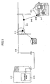
- FIG.1 shows an exemplary configuration of a PLC communication system.
- the power line consists of a 6.6 kV high voltage power distribution line 9-2 arranged between a power distribution substation 9-1 and a pole transformer 9-3, a 100V/200V low voltage power distribution line 9-4 arranged between the pole transformer 9-3 and a house 9-6, and an incoming line 9-5.
- optical fibers are provided between the access node 9-11 of the power distribution substation 9-1 and the modem provided in the pole transformer 9-3, along with the above high voltage power distribution line 9-2, so that data transmission by optical signals is made possible within this region. Also, data transmission is possible in between the pole transformer 9-3 and a modem plugged into an outlet in the house 9-6 via the 100V/200V low voltage distribution line 9-4, the incoming line 9-5, and interior wiring 9-7.
- data transmission may be performed using communication techniques that are known to be resistant to noise such as the FM modulation technique, the FSK modulation technique, the PSK modulation technique, or the spread spectrum technique.
- communication may be established by introducing the multi-carrier modulation technique, the OFDM (Orthogonal Frequency Division Multiplexing) technique, or the like so that carrier bands with high noise levels can be avoided.
- OFDM Orthogonal Frequency Division Multiplexing
- the electromagnetic fields due to radiation leakage from the power lines that carry the signals may influence other communications and broadcast media.
- the power lines of the PLC communication system may generate noise that debilitates receivers of shortwave broadcasts in receiving clear shortwave broadcasts.
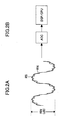
- FIG.2A shows an exemplary state of a signal received at the modem implemented in the pole transformer 9-3 via the low voltage power distribution line 9-4 in the PLC communication system of FIG.1.
- the received signal is a superimposition of the data transmission signal RS with a small amplitude on a noise level RN with a large amplitude.
- the composite signal of the noise level RN and the received signal RS must be input to an A/D converter (ADC) over the entire range of amplitude RIN. Then, the digitalized signal is processed by a digital signal processor (DSP), as shown in FIG.2B.
- ADC A/D converter
- DSP digital signal processor
- the amplitude RIN of the composite signal is large and thus, no A/D converter currently manufactured is capable of handling such a large dynamic range (over 130dB). Thus, it is quite difficult to realize a circuit that is capable of directly taking in the signal received via the power line.
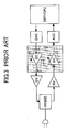
- FIG.3 illustrates one technique to solve the above-described problem concerning the dynamic range of the input signal.
- a gain controller (GC) is provided before the A/D converter (ADC) and the amplitude of the input signal is attenuated by the gain controller (GC) so as to conform to the dynamic range of the A/D converter (ADC).
- a receiving circuit can be realized using a general-purpose A/D converter (ADC).
- the gain controller GC
- the amplitude of the data transmission signal RS containing the transmission data is also attenuated.
- the precision of transmission data detection is degraded, thereby causing the degradation of reception characteristics.
- EP-A-0 496 717 there is disclosed a method and device for transmitting data within a predetermined frequency range over a noisy medium, wherein a spread spectrum data independent signal formed by a pseudo noise code is mixed with the data to be transmitted for forming a spread spectrum data signal, which data signal is modulated and at least 50% of the power of the modulated data signal is transmitted within said frequency range.
- the chip of the data signal to be transmitted is substituted by a wave shaped signal having a raised cosine spectrum, which wave shaped signal is thereafter truncated by means of a truncation window whereby the spectrum broadening is kept limited within said frequency range in order to obtain a further wave shaped signal which is, considered in the time domain, limited within the time of a predetermined period.
- the present invention has been developed in response to the above-described problems of the related art and its object is to provide a data reception method that enables precise data regeneration from an input signal that has a large noise amplitude using an A/D converter that has a relatively narrow dynamic range.
- a data transmission apparatus comprising a transmission side and a reception side, characterized in that the reception side includes: a spread spectrum processing part that performs a spread spectrum process on an input signal; an analog-to-digital conversion part that performs an analog-to-digital conversion process on a signal that has undergone said spread spectrum process; and an inverse spread spectrum processing part that performs an inverse spread spectrum process of said spread spectrum process on a signal that has undergone said analog-to-digital conversion process.
- a data transmission method for performing data transmission in a data transmission apparatus comprising a transmission side and a reception side, comprising, on the reception side: a spread spectrum processing step of performing a spread spectrum process on an input signal; an analog-to-digital conversion step of performing an analog-to-digital conversion process on a signal that has undergone said spread spectrum process; and an inverse spread spectrum processing step of performing an inverse spread spectrum process of said spread spectrum process on a signal that has undergone said analog-to-digital conversion process.
- a spread spectrum process is performed through multiplication of an input signal by a PN sequence, and the signal obtained from the spread spectrum process is digitally converted by an analog-to-digital conversion process. Further, an inverse spread spectrum process of the above spread spectrum process is performed through multiplication of the digitally converted signal by the same PN sequence.
- the precision of the analog-to-digital conversion process can be substantially improved.
- transmission data contained in the input signal can be regenerated with precision as a digital signal using a general-purpose A/D converter that has a relatively narrow dynamic range.
- FIG.4 shows an exemplary configuration of the modem implemented at the pole transformer 9-3 or at the terminating portion of the internal wiring 9-7 in the house 9-6 of FIG.1, as a data transmission apparatus according to an embodiment of the present invention.
- a scrambler (SCR, S/P) 11 performs a scramble process on a transmitted signal (SD), and also converts this signal from a serial signal to a parallel signal, the resulting signal being sent to a vector summation circuit (G/N, SUM) 12.
- SD transmitted signal
- G/N, SUM vector summation circuit
- the vector summation circuit 12 converts the input parallel signal having a grey binary code (G) into a signal with a natural binary code (N) , and computes a vector component summation, which is a counterpart process performed by a vector differential circuit (DIF, N/G) 29 for phase detection at the receiving side. Then, the resulting signal is sent to a signal point generator 13.
- G grey binary code
- N natural binary code
- the signal point generator 13 divides the input transmitted data into multiple portions, each having predetermined number of bits, based on predetermined modulation block units, and generates one signal point for each portion corresponding to the number of bits. Then a zero point signal is inserted into the transmitted signal made up of these signal points by a zero point inserter 14. Then a waveform is shaped by a roll off filter (ROF1) 15 in accordance with the limitations on the available frequency band in the power line carrier communication. Further, the transmitted signal is modulated by a modulation circuit (MOD) 16, and converted from a digital signal to an analog signal by a D/A conversion circuit (D/A) 17. Then, a low frequency signal component covering the frequency band of the power line carrier wave is extracted by a low pass filter (LPF) 18, and this is sent onto a transmission line TX-line.
- MOD modulation circuit
- D/A D/A conversion circuit
- the transmitted signal sent via the transmission line TX-line is received by a counterpart modem (e.g. the modem implemented at the terminating portion of the internal wiring 9-7 in the house 9-6 as a counterpart of the modem implemented at the pole transformer 9-3 of FIG.1) through a receiving line RX-line and a band pass filter (BPF) 21 extracts only a predetermined frequency band component therefrom.
- BPF band pass filter
- the resulting signal is then converted back to a digital signal by an A/D conversion circuit (A/D) 22.
- This digitalized signal is converted into a base band signal by a demodulation circuit (DEM) 23 and the waveform is shaped by a roll off filter (ROF2) 24. Then the output signal is sent to a VCXO (Voltage Controlled Crystal Oscillator) type phase lock loop circuit (PLL-VCXO) 31.
- DEM demodulation circuit
- ROF2 roll off filter
- PLL-VCXO Voltage Controlled Crystal Oscillator
- the VCXO type phase lock loop circuit 31 extracts the phases of the zero points in the signal and supplies the phases of these zero points as a sampling timing signal to the A/D conversion circuit (A/D) 22 and a clock (RX-CLK) distribution part 32.
- the output signal of the roll off filter (ROF2) 24 of the reception side goes through a zero point deletion part 25 where the zero points in the signal are deleted.
- an automatic gain controller (AGC) 26 controls the signal gain at a predetermined level and an automatic carrier phase controller (CAPC) 27 performs phase adjustment on the signal.
- a determination circuit (DEC) 28 determines the reception signal and the determination result is output to the vector component differential circuit (DIF, N/G) 29.
- the vector differential circuit (DIF, N/G) 29 computes a vector difference for the signal containing the natural binary code sent from the vector summation circuit (G/N, SUM) 12 of the transmission side, which is an inverse process of the computation performed by the vector summation circuit (G/N, SUM) 12. Then the signal is converted back to a signal with a grey binary code (G) , and sent to a descrambler (P/S, DSCR) 31. The descrambler 31 converts this parallel grey code signal to a serial signal and performs a descramble process to obtain received data (RD).
- DIF, N/G computes a vector difference for the signal containing the natural binary code sent from the vector summation circuit (G/N, SUM) 12 of the transmission side, which is an inverse process of the computation performed by the vector summation circuit (G/N, SUM) 12. Then the signal is converted back to a signal with a grey binary code (G) , and sent to a des
- a transmission clock distribution circuit (TX-CLK) 19 distributes a transmission clock signal to the zero point insertion part 14, the D/A converter (D/A) 17, and other transmission circuits.
- the reception clock (RX-CLK) distribution part 32 extracts a reception clock signal from the VCXO type phase lock loop circuit (PLL-VCXO) 31 and distributes this reception clock signal to the zero point deletion part 25 and other reception circuits.
- reception clock (RX-CLK) distribution part 32 is merely a passage way for the sampling timing signal indicating the phase of the zero points extracted from the VCXO type phase lock loop circuit (PLL-VCXO) 31, and this signal is simply a symbolic timing signal.
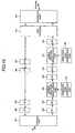
- FIG.5 is a block diagram showing an internal circuit configuration of the A/D conversion circuit 22 of the reception side shown in FIG.4.
- the input signal that has undergone the frequency band limitation process at the band pass filter 21 has a waveform as shown in FIG.2A, for example.
- the amplitude of the input signal is attenuated so as to conform to the dynamic range of the A/D converter 54.
- this signal is multiplied by a predetermined PN (pseudonoise) sequence supplied by a PN sequence generator 57 at a multiplier 52, and a spread spectrum process is performed by high speed sampling.
- PN pseudonoise
- ⁇ PN sequence' is used as a general term for referring to the spreading codes by which a signal for modulation is multiplied in the spread spectrum process .
- the spreading codes may be, for example, M sequence codes, Gold sequence codes, Wavelet sequence codes, Hadamard sequence codes, etc.
- the signal is input to the A/D converter 54 where an analog-to-digital conversion is performed.
- This process also involves high speed sampling so that the resolution of the A/D converter 54 can be improved (however, with a low bit rate).
- an inverse spread spectrum process is performed at a multiplier 55 by multiplying the input signal by the same PN sequence supplied from the PN sequence generator 57.
- the multiplication in this spread spectrum process is performed using multi-chip PN sequences as in the multiplier 52.
- the inverse spread spectrum process also involves high speed sampling (however, with a low bit rate).
- FIGS.6A-6F show the changes in the waveform of the signal at each point in the circuit configuration of FIG.5.
- an analog input signal a (t) made up of a reception signal superimposed on a noise signal as shown in FIG.6B is multiplied by a PN sequence c(t) shown in FIG.6C at a multiplier 52.
- the resulting analog signal a(t)*c(t) goes through the low pass filter 53 and is digitally converted at the A/D converter 54 to obtain a digital signal a (t)*c(t)*A/D.
- the digitalized signal a(t)*A/D corresponding to the input analog signal a(t) can be obtained.
- the ⁇ PN sequence number' refers to the number of chips in each cycle of the PN sequence.
- the number of bits required in detecting the entire range is 22 bits.
- the PN sequence number required in order to secure bits over 22 is 65,535 as shown in the following table chart 1.
- N PN Number of bits in ADC Increased number of bits (n) in ADC Total number of bits 31 14 2.5 16.5 63 14 3 17 127 14 3.5 17.5 255 14 4 18 511 14 4.5 18.5 1023 14 5 19 2047 14 5.5 19.5 4095 14 6 20 8191 14 6.5 20.5 16383 14 7 21 32767 14 7.5 21.5 65535 14 8 22
- the final resolution obtained by the multiplication of the PN sequence can be calculated from the formula below:
- the resolution of the A/D converter 54 needs to be increased by 8 bits from the original resolution of 14 bits.
- the bottom column in the table chart 1 is used and the multiplication needs to be performed using the PN sequence with the PN sequence number 65,535 at each of the multipliers 52 and 55.
- FIG.7A corresponds to the input waveform shown in FIG.6B
- FIG.7B corresponds to the PN sequence waveform shown in FIG.6C
- FIG.7C corresponds to the signal waveform after the PN sequence multiplication process shown in FIG.6D
- FIG.7D shows the sampling timing in the A/D converter 54
- FIG.7E corresponds to the signal extracted at the A/D converter 54 as shown in FIG.6E.
- FIGS.8A-8C show exemplary signal waveforms in the conventional art where the spread spectrum process using the PN sequence is not implemented.
- FIG.8A shows the same original signal as that in FIG.7A;
- FIG.8B shows the sampling timing of a conventional A/D converter;
- FIG.8C shows the waveform extracted at the A/D converter.
- the input waveform is multiplied by the PN sequence and the sampling timing of the A/D converter 54 is also increased corresponding to the multiplication result.
- the sampling timing of the conventional A/D converter is the same as the bit rate of the PN sequence used in the present embodiment.
- the PN sequence number of the PN sequence is the number of chips in each cycle of the PN sequence.
- the sampling timing of the A/D converter is also increased by a multiplying number that is equivalent to the PN sequence number, the rate of improvement in the bit rate.
- a multiplying number that is equivalent to the PN sequence number, the rate of improvement in the bit rate.
- sampling by the A/D converter 54 is performed at a timing identical to the oscillation timing of the original signal that is oscillated in both positive and negative directions as a result of the multiplication using the PN sequence .
- sampling by the A/D converter 54 is performed at a timing identical to the oscillation timing of the original signal that is oscillated in both positive and negative directions as a result of the multiplication using the PN sequence .
- a highly precise signal extraction is possible by the A/D converter 54.
- the ratio of the signal power to the noise power (S/N) is equal to the PN sequence number N PN is explained.
- quantized noise which is the determining factor of the S/N ratio of the A/D converter, is proportional to the sampling frequency of the A/D converter.
- the S/N ratio can be improved by 3 dB.
- the underlying principles of this formula are explained in, for example, PMC Communication Technology , Kaneko, Sangyo Shuppan, Ltd.
- the resolution of the A/D converter 54 can be substantially improved by performing a spread spectrum process wherein high speed sampling is performed on the input signals in the A/D conversion circuit 22.
- a data transmission apparatus that prevents the degradation of reception signal detection performance is realized.
- a gain controller has conventionally been implemented before the general-purpose A/D converter so as to attenuate the signal amplitude.
- FRS stands for 'full scale range'.
- FIGS.9A and 9B illustrate a more generalized system in which the embodiment of the present invention can be implemented.
- the modem functioning as the data transmission apparatus of the present embodiment corresponds to a power line carrier modem, which is the terminal portion of the power line carrier communication system realized by power lines as shown in FIG.9A.
- the power line carrier modem is characterized by an A/D conversion circuit portion indicated by hatched lines in FIG.9B.
- This A/D conversion circuit may have the configuration of the A/D conversion circuit 22 shown in FIG.5 wherein a general-purpose A/D converter 54 is used to perform high speed sampling using a PN sequence in a spread spectrum process.
- a general-purpose A/D converter 54 is used to perform high speed sampling using a PN sequence in a spread spectrum process.
- FIG.10 is a block diagram showing a circuit configuration of a data transmission apparatus according to another embodiment of the present invention.
- This data transmission apparatus may correspond to the modem shown in FIG.9B.
- the input signal received via the power line is supplied to a spread spectrum modulation part 154 via a coupling part 151 that extracts the signal carried by the power carrier line, a receiving part 152 that extracts the desired signal components, and a gain controller 153 that controls the amplitude of the signal.
- the input signal is multiplied by the PN sequence to perform the spread spectrum modulation.
- a spreading code generation part 159 generates the PN sequence and supplies this to the spread spectrum modulation part 154.
- the above modulated signal goes through a low pass filter 155 where unnecessary high frequency components are removed, after which the signal is converted into a digital signal at an A/D converter 156. Then, at a spread spectrum demodulation part 157, the same PN sequence is multiplied to perform despreading.
- a spreading code generation part 160 generates the PN sequence and supplies this to the spread spectrum demodulation part 157.
- signals received via other networks undergo a predetermined interface process at the interface part 141, after which a predetermined process is performed at the digital signal processing part 142. Then, the digital signal is converted into an analog signal at a D/A converter 143. Next, this analog signal passes through a low pass filter 144 where unnecessary high frequency components are removed, after which the amplitude of this signal is adjusted at a gain controller 145. Then, the amplitude of the signal is increased at a drive part 146 and the resulting signal is sent to the coupling part 151 for transmission via the power line.
- the gain controller 153, the spread modulation part 154, the low pass filter 155, A/D converter 156, the spread demodulation part 157, the low pass filter 158, and the spreading code generation parts 159 and 160 correspond to the gain controller 51, the multiplier 52, the low pass filter 53, the A/D converter 54, the multiplier 55, the low pass filter 56 and the PN sequence generation part 57, respectively, and identical processes are performed in each of the corresponding parts.
- the performance of the analog-to-digital conversion can be substantially improved.
- transmission data contained in an input signal can be accurately regenerated as a digital signal even with a general-purpose A/D converter having a relatively narrow dynamic range.
Landscapes
- Engineering & Computer Science (AREA)
- Power Engineering (AREA)
- Computer Networks & Wireless Communication (AREA)
- Signal Processing (AREA)
- Analogue/Digital Conversion (AREA)
- Compression, Expansion, Code Conversion, And Decoders (AREA)
Claims (9)
- Dispositif de transmission de données comprenant un côté émission et un côté réception, caractérisé en ce que le côté de réception comprend :une partie de traitement d'étalement de spectre (52) qui exécute un traitement d'étalement de spectre sur un signal d'entrée,une partie de conversion d'analogique en numérique (54) qui exécute un traitement de conversion d'analogique en numérique sur un signal qui a subi ledit traitement d'étalement de spectre, etune partie de traitement d'étalement de spectre inverse (55) qui exécute un traitement d'étalement de spectre inverse dudit traitement d'étalement de spectre sur un signal qui a subi ledit traitement de conversion d'analogie en numérique.
- Dispositif de transmission de données selon la revendication 1, dans lequel ledit traitement d'étalement de spectre est exécuté en utilisant une séquence de pseudo-bruit PN prédéterminée (57).
- Dispositif de transmission de données selon la revendication 2, dans lequel un numéro de séquence de pseudo-bruit PN de ladite séquence de pseudo-bruit PN est établi a une valeur qui augmente un nombre de bits pour ledit traitement de conversion d'analogique en numérique a un nombre de bits requis pour la détection de données de transmission contenues dans le signal d'entrée avec une précision prédéterminée.
- Dispositif de transmission de données selon la revendication 1, comprenant en outre :une partie de commande de gain (51) qui exécute un traitement de commande de gain sur un signal d'entrée, oùladite partie de traitement d'étalement de spectre (52) exécute un traitement d'étalement de spectre sur un signal qui a subi ledit traitement de commande de gain de signal.
- Système de communications à courants porteurs sur ligne électrique, comprenant :une ligne électrique fonctionnant en tant que trajet de transmission de données pour transmettre des données, etun dispositif de transmission de données selon la revendication 1 qui termine ladite ligne électrique.
- Procédé de transmission de données, destiné à effectuer une transmission de données dans un dispositif de transmission de données comprenant un côté d'émission et un côté de réception, comprenant, du côté de réception :une étape de traitement d'étalement de spectre (52) consistant à exécuter un traitement d'étalement de spectre sur un signal d'entrée,une étape de conversion d'analogique en numérique (54) consistant à exécuter un traitement de conversion d'analogique en numérique sur un signal qui a subi ledit traitement d'étalement de spectre, etune étape de traitement d'étalement de spectre inverse (55) consistant à exécuter un traitement d'étalement de spectre inverse dudit traitement d'étalement de spectre sur un signal qui a subi ledit traitement de conversion d'analogique en numérique.
- Procédé de transmission de données selon la revendication 6, dans lequel ledit traitement d'étalement de spectre est exécuté en utilisant une séquence de pseudo-bruit PN prédéterminée (57) dans ladite étape de traitement d'étalement de spectre.
- Procédé de transmission de données selon la revendication 7, dans lequel un numéro de séquence de pseudo-bruit PN de ladite séquence de pseudo-bruit PN est établie à une valeur qui augmente un nombre de bits pour ledit traitement de conversion d'analogique en numérique à un nombre de bits requis pour la détection de données de transmission contenues dans le signal d'entrée avec une précision prédéterminée.
- Procédé de transmission de données selon la revendication 6, comprenant en outre :une étape de commande de gain (51) consistant à exécuter un traitement de commande de gain de signal sur un signal d'entrée, oùle traitement d'étalement de spectre de ladite étape de traitement d'étalement de spectre (52) est exécuté sur un signal qui a subi ledit traitement de commande de gain de signal.
Applications Claiming Priority (2)
| Application Number | Priority Date | Filing Date | Title |
|---|---|---|---|
| JP2002243578A JP3440095B1 (ja) | 2002-08-23 | 2002-08-23 | データ伝送装置及びデータ伝送方法 |
| JP2002243578 | 2002-08-23 |
Publications (2)
| Publication Number | Publication Date |
|---|---|
| EP1392002A1 EP1392002A1 (fr) | 2004-02-25 |
| EP1392002B1 true EP1392002B1 (fr) | 2007-11-07 |
Family
ID=27785594
Family Applications (1)
| Application Number | Title | Priority Date | Filing Date |
|---|---|---|---|
| EP20030016577 Expired - Lifetime EP1392002B1 (fr) | 2002-08-23 | 2003-07-25 | Système de communication sur ligne de courant |
Country Status (4)
| Country | Link |
|---|---|
| US (1) | US20040125860A1 (fr) |
| EP (1) | EP1392002B1 (fr) |
| JP (1) | JP3440095B1 (fr) |
| DE (1) | DE60317279T2 (fr) |
Families Citing this family (12)
| Publication number | Priority date | Publication date | Assignee | Title |
|---|---|---|---|---|
| US7542505B2 (en) * | 2003-10-20 | 2009-06-02 | Northrop Grumman Corporation | Systems and methods for signal conversion |
| US7599348B2 (en) * | 2003-11-04 | 2009-10-06 | Lg Electronics Inc. | Digital E8-VSB reception system and E8-VSB data demultiplexing method |
| US7660342B2 (en) * | 2005-05-04 | 2010-02-09 | Stmicroelectronics (Rousset) Sas | Digital receiver device based on an input comparator |
| JP4635947B2 (ja) | 2005-10-12 | 2011-02-23 | パナソニック株式会社 | 電力線通信装置、集積回路、及び電力線通信方法 |
| DE102008050045B4 (de) * | 2008-06-24 | 2012-09-27 | Deutsches Zentrum für Luft- und Raumfahrt e.V. | Verfahren und Vorrichtung zur Übertragung von Daten über eine elektrische Stromversorgungsleitung |
| MX2011002310A (es) * | 2008-08-28 | 2011-08-03 | Aclara Power Line Systems Inc | Metodo general para la transmision de datos de baja frecuencia en una linea de energia. |
| JP2010273307A (ja) * | 2009-05-25 | 2010-12-02 | Canon Inc | 信号伝送装置 |
| CN102158299B (zh) * | 2010-11-19 | 2015-05-27 | 中国电力科学研究院 | 一种工频通信多路传输正交编码方法 |
| KR101773612B1 (ko) | 2011-01-13 | 2017-08-31 | 삼성전자주식회사 | 터치 영역 확인 장치 및 방법 |
| US9077363B2 (en) | 2013-12-03 | 2015-07-07 | Analog Devices, Inc. | Stochastic encoding in analog to digital conversion |
| US11888548B2 (en) | 2021-05-28 | 2024-01-30 | Massachusetts Institute Of Technology | Power line communication for low-bandwidth control and sensing |
| CN117572169B (zh) * | 2023-11-20 | 2024-05-14 | 浙江大学 | 一种基于超声数据处理技术进行局放检测的方法及探头 |
Family Cites Families (6)
| Publication number | Priority date | Publication date | Assignee | Title |
|---|---|---|---|---|
| US5448593A (en) * | 1984-03-06 | 1995-09-05 | Cyplex Corporation | Frequency hopping time-diversity communications systems and transceivers for local area networks |
| BE1005232A3 (nl) * | 1991-01-21 | 1993-06-01 | Vynckier Nv | Werkwijze en inrichting voor het over een ruisrijk medium overdragen van data. |
| US5564097A (en) * | 1994-05-26 | 1996-10-08 | Rockwell International | Spread intermediate frequency radio receiver with adaptive spurious rejection |
| JPH1070780A (ja) * | 1996-08-27 | 1998-03-10 | Uniden Corp | データ収集システム |
| JP4303373B2 (ja) * | 1999-09-14 | 2009-07-29 | 株式会社日立コミュニケーションテクノロジー | 無線基地局装置 |
| JP2001237902A (ja) | 2000-02-24 | 2001-08-31 | Mitsubishi Electric Corp | 受信機 |
-
2002
- 2002-08-23 JP JP2002243578A patent/JP3440095B1/ja not_active Expired - Fee Related
-
2003
- 2003-07-23 US US10/626,432 patent/US20040125860A1/en not_active Abandoned
- 2003-07-25 DE DE2003617279 patent/DE60317279T2/de not_active Expired - Fee Related
- 2003-07-25 EP EP20030016577 patent/EP1392002B1/fr not_active Expired - Lifetime
Also Published As
| Publication number | Publication date |
|---|---|
| US20040125860A1 (en) | 2004-07-01 |
| DE60317279T2 (de) | 2008-09-04 |
| JP2004088222A (ja) | 2004-03-18 |
| EP1392002A1 (fr) | 2004-02-25 |
| DE60317279D1 (de) | 2007-12-20 |
| JP3440095B1 (ja) | 2003-08-25 |
Similar Documents
| Publication | Publication Date | Title |
|---|---|---|
| EP1376889B1 (fr) | Suppression du signal pilote et des signaux de trafic indesirables dans un système AMCR | |
| US6320897B1 (en) | Multicode spread spectrum communications system | |
| EP0727115B1 (fr) | Multiplexage en quadrature de deux signaux de donnees a spectre etale par differentes sequences de bruit pseudo-aleatoire | |
| CA2188869C (fr) | Detecteur coherent de liaison montante dans un systeme d'acces multiple par difference de code a sequence directe | |
| EP1392002B1 (fr) | Système de communication sur ligne de courant | |
| US6671307B2 (en) | Spread-spectrum high data rate system and method | |
| JPH04296126A (ja) | Cdmaスペクトル拡散無線伝送システムにおける無線信号の受信装置 | |
| US6529560B1 (en) | System and method to reduce the peak-to-average power ratio in a DS-CMDA transmitter | |
| EP1097520A2 (fr) | Recepteur cdma ameliore et son procede de fonctionnement | |
| EP0589683B1 (fr) | Procédé pour modulation à étalement de spectre par un peigne de fréquences | |
| KR100423724B1 (ko) | 무선통신시스템에서 복합 직교 위상 편이 방식을 이용한데이터 처리 장치 및 그 방법 | |
| HK1063111B (en) | Cancellation of pilot and unwanted traffic signals in a cdma system | |
| HK1038450B (en) | Cancellation of pilot and unwanted traffic signals in a cdma system | |
| HK1050780A (en) | Complex quadrature phase shift keying | |
| HK1061612B (en) | Cancellation of pilot and unwanted traffic signals in a cdma system | |
| HK1014300B (en) | A direct sequence cdma coherent uplink detector | |
| HK1015211B (en) | Quadrature multiplexing of two data signals spread by different pn-sequences |
Legal Events
| Date | Code | Title | Description |
|---|---|---|---|
| PUAI | Public reference made under article 153(3) epc to a published international application that has entered the european phase |
Free format text: ORIGINAL CODE: 0009012 |
|
| AK | Designated contracting states |
Kind code of ref document: A1 Designated state(s): AT BE BG CH CY CZ DE DK EE ES FI FR GB GR HU IE IT LI LU MC NL PT RO SE SI SK TR |
|
| AX | Request for extension of the european patent |
Extension state: AL LT LV MK |
|
| 17P | Request for examination filed |
Effective date: 20040817 |
|
| AKX | Designation fees paid |
Designated state(s): DE FR GB |
|
| 17Q | First examination report despatched |
Effective date: 20051005 |
|
| GRAP | Despatch of communication of intention to grant a patent |
Free format text: ORIGINAL CODE: EPIDOSNIGR1 |
|
| GRAS | Grant fee paid |
Free format text: ORIGINAL CODE: EPIDOSNIGR3 |
|
| GRAA | (expected) grant |
Free format text: ORIGINAL CODE: 0009210 |
|
| AK | Designated contracting states |
Kind code of ref document: B1 Designated state(s): DE FR GB |
|
| REG | Reference to a national code |
Ref country code: GB Ref legal event code: FG4D |
|
| REF | Corresponds to: |
Ref document number: 60317279 Country of ref document: DE Date of ref document: 20071220 Kind code of ref document: P |
|
| ET | Fr: translation filed | ||
| PLBE | No opposition filed within time limit |
Free format text: ORIGINAL CODE: 0009261 |
|
| STAA | Information on the status of an ep patent application or granted ep patent |
Free format text: STATUS: NO OPPOSITION FILED WITHIN TIME LIMIT |
|
| 26N | No opposition filed |
Effective date: 20080808 |
|
| PGFP | Annual fee paid to national office [announced via postgrant information from national office to epo] |
Ref country code: FR Payment date: 20090710 Year of fee payment: 7 |
|
| PGFP | Annual fee paid to national office [announced via postgrant information from national office to epo] |
Ref country code: DE Payment date: 20090723 Year of fee payment: 7 Ref country code: GB Payment date: 20090722 Year of fee payment: 7 |
|
| GBPC | Gb: european patent ceased through non-payment of renewal fee |
Effective date: 20100725 |
|
| REG | Reference to a national code |
Ref country code: FR Ref legal event code: ST Effective date: 20110331 |
|
| PG25 | Lapsed in a contracting state [announced via postgrant information from national office to epo] |
Ref country code: DE Free format text: LAPSE BECAUSE OF NON-PAYMENT OF DUE FEES Effective date: 20110201 |
|
| REG | Reference to a national code |
Ref country code: DE Ref legal event code: R119 Ref document number: 60317279 Country of ref document: DE Effective date: 20110201 |
|
| PG25 | Lapsed in a contracting state [announced via postgrant information from national office to epo] |
Ref country code: FR Free format text: LAPSE BECAUSE OF NON-PAYMENT OF DUE FEES Effective date: 20100802 |
|
| PG25 | Lapsed in a contracting state [announced via postgrant information from national office to epo] |
Ref country code: GB Free format text: LAPSE BECAUSE OF NON-PAYMENT OF DUE FEES Effective date: 20100725 |